

Page 1
SEMICONDUCTOR TECHNICAL DATA
The RF Line
. . . designed primarily for wideband large–signal output and driver amplifier
stages in the 30 to 500 MHz frequency range.
• Specified 28 Volt, 500 MHz Characteristics —
Output Power = 100 W
Typical Gain = 9.5 dB (Class AB); 8.5 dB (Class C)
Efficiency = 55% (Typ)
• Built–In Input Impedance Matching Networks for Broadband Operation
• Push–Pull Configuration Reduces Even Numbered Harmonics
• Gold Metallization System for High Reliability
• 100% Tested for Load Mismatch
2
6
5, 8
1, 4
Order this document
by MRF393/D
100 W, 30 to 500 MHz
CONTROLLED “Q”
BROADBAND PUSH–PULL
RF POWER TRANSISTOR
NPN SILICON
7
3
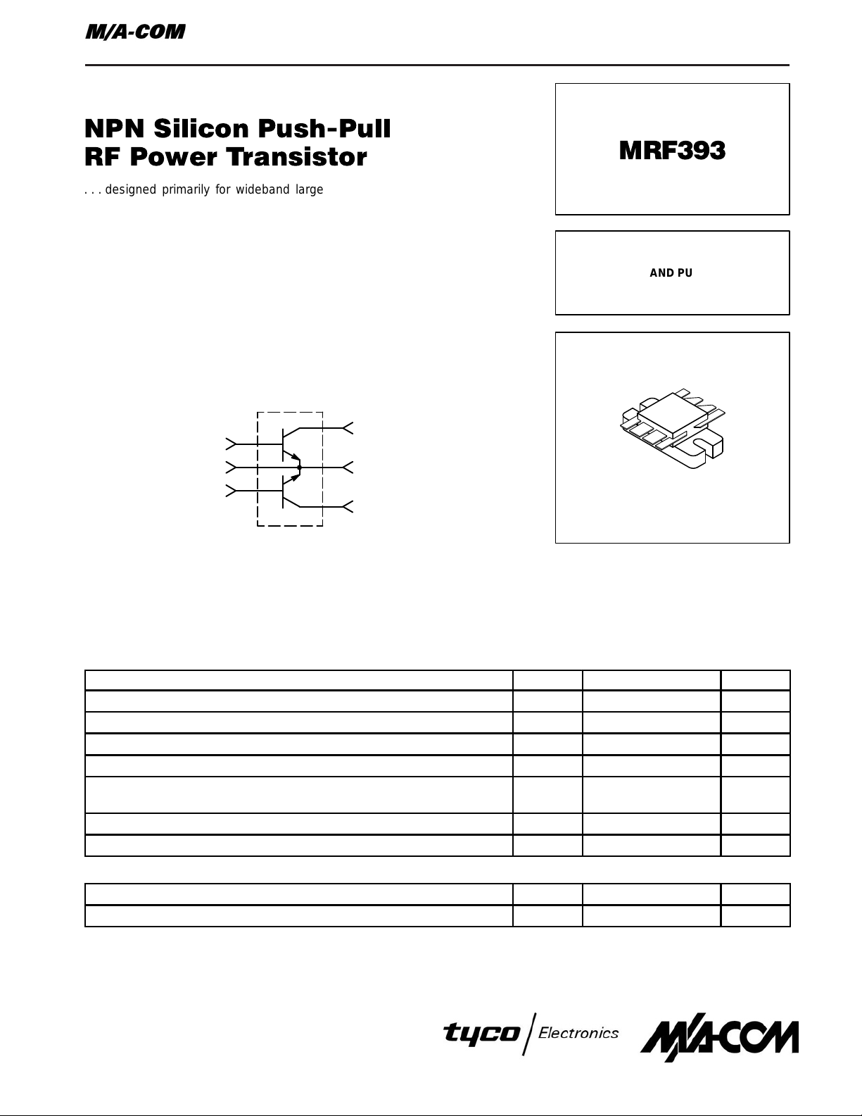
The MRF393 is two transistors in a single package with separate base and collector leads
and emitters common. This arrangement provides the designer with a space saving
device capable of operation in a push–pull configuration.
CASE 744A–01, STYLE 1
PUSH–PULL TRANSISTORS
MAXIMUM RATINGS
Rating Symbol Value Unit
Collector–Emitter Voltage V
Collector–Base Voltage V
Emitter–Base Voltage V
Collector Current — Continuous I
Total Device Dissipation @ TC = 25°C (1)
Derate above 25°C
Storage Temperature Range T
Junction Temperature T
CEO
CBO
EBO
C
P
D
stg
J
30 Vdc
60 Vdc
4.0 Vdc
16 Adc
270
1.54
–65 to +150 °C
200 °C
THERMAL CHARACTERISTICS
Characteristic Symbol Max Unit
Thermal Resistance, Junction to Case R
NOTE:
1. This device is designed for RF operation. The total device dissipation rating applies only when the device is operated as an RF push–pull
amplifier.
θJC
0.65 °C/W
Watts
W/°C
REV 7
1
Page 2
ELECTRICAL CHARACTERISTICS (T
Characteristic Symbol Min Typ Max Unit
= 25°C unless otherwise noted.)
C
OFF CHARACTERISTICS (1)
Collector–Emitter Breakdown V oltage (IC = 50 mAdc, IB = 0) V
Collector–Emitter Breakdown Voltage (IC = 50 mAdc, VBE = 0) V
Emitter–Base Breakdown Voltage (IE = 5.0 mAdc, IC = 0) V
Collector Cutoff Current (VCB = 30 Vdc, IE = 0) I
ON CHARACTERISTICS (1)
DC Current Gain (IC = 1.0 Adc, VCE = 5.0 Vdc) h
DYNAMIC CHARACTERISTICS (1)
Output Capacitance (VCB = 28 Vdc, IE = 0, f = 1.0 MHz) C
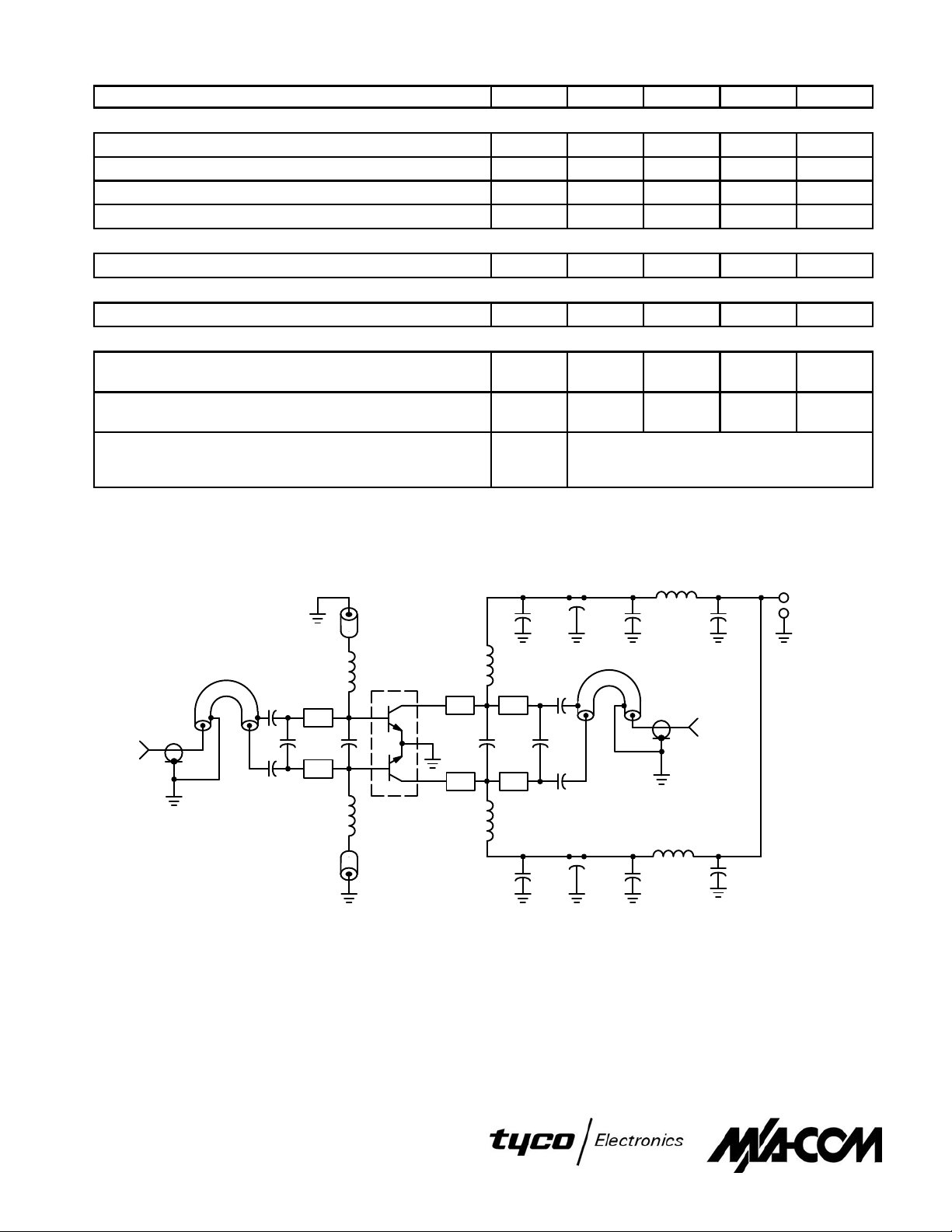
FUNCTIONAL TESTS (2) — See Figure 1
Common–Emitter Amplifier Power Gain
(VCC = 28 Vdc, P
Collector Efficiency
(VCC = 28 Vdc, P
Load Mismatch
(VCC = 28 Vdc, P
VSWR = 30:1, all phase angles)
NOTES:
1. Each transistor chip measured separately.
2. Both transistor chips operating in push–pull amplifier.
= 100 W, f = 500 MHz)
out
= 100 W, f = 500 MHz)
out
= 100 W, f = 500 MHz,
out
(BR)CEO
(BR)CES
(BR)EBO
CBO
FE
ob
G
pe
η 50 55 — %
ψ
30 — — Vdc
60 — — Vdc
4.0 — — Vdc
— — 5.0 mAdc
20 — 100 —
40 75 95 pF
7.5 8.5 — dB
No Degradation in Output Power
B1
C1
C2
C1, C2, C7, C8 — 240 pF 100 mil Chip Cap
C3 — 15 pF 100 mil Chip Cap
C4 — 24 pF 100 mil Chip Cap
C5 — 33 pF 100 mil Chip Cap
C6 — 12 pF 100 mil Chip Cap
C9, C13 — 1000 pF 100 mil Chip Cap
C10, C14 — 680 pF Feedthru Cap
C11, C15 — 0.1 µF Ceramic Disc Cap
C12, C16 — 50 µF 50 V
L1
Z1
C4C3
Z2
L2
D.U.T.
C15
L5
C12
L6
C16
C10
C9 C11
L3
Z3 Z5
C5
Z4 Z6
L4
L1
,
L2 — 0.15 µH Molded Choke with Ferrite Bead
L3
,
L4 — 2–1/2 Turns #20 AWG 0.200″ ID
L5
,
L6 — 3–1/2 Turns #18 AWG 0.200″ ID
B1, B2 — Balun 50 Ω Semi Rigid Coax, 86 mil OD, 4″ Long
Z1, Z2 — 850 mil Long x 125 mil W. Microstrip
Z3, Z4 — 200 mil Long x 125 mil W. Microstrip
Z5, Z6 — 800 mil Long x 125 mil W. Microstrip
Board Material — 0.0325″ Teflon–Fiberglass, εr = 2.56,
Board Material — 1 oz. Copper Clad both sides.
C7
C6
C8
C13
B2
C14
+ 28 V
REV 7
2
Figure 1. 500 MHz T est Fixture
Page 3

CLASS C
140
120
100
80
60
40
out
P , OUTPUT POWER (WATTS)
20
120
100
80
f = 100 MHz 225 MHz
400 MHz
70
f = 100 MHz
60
80
500 MHz
50
40
30
20
out
P , OUTPUT POWER (WATTS)
VCC = 28 V
0
Pin, INPUT POWER (WATTS)
10
20181614121086420
0
Pin, INPUT POWER (WATTS)
Figure 2. Output Power versus Input Power Figure 3. Output Power versus Input Power
CLASS C
Pin = 10 W
8 W
6 W
120
Pin = 16 W
100
80
225 MHz
400 MHz
500 MHz
VCC = 13.5 V
20181614121086420
12 W
8 W
60
out
40
P , OUTPUT POWER (WATTS)
20
12
f = 225 MHz
16 20 24 28
VCC, SUPPLY VOLTAGE (VOL TS)
60
out
40
P , OUTPUT POWER (WATTS)
20
12
f = 500 MHz
16 20 24 28
VCC, SUPPLY VOLTAGE (VOL TS)
Figure 4. Output Power versus Supply Voltage Figure 5. Output Power versus Supply Voltage
ZOL* = Conjugate of the optimum load impedance
ZOL* = into which the device output operates at a
2
4
ZOL*
f = 100 MHz
f = 100 MHz
2
400
4
225
6
Zo = 20
Ω
8
NOTE: Zin & ZOL* are given from base–to–base
NOTE: and collector–to–collector respectively.
ZOL* = given output power, voltage and frequency.
2
4
500
500
225
Z
in
6
400
VCC = 28 V, P
f MHz Z
0.85 + j0
100
0.58 + j2.6
225
3.00 + j5.9
400
4.80 + j3.0
500
8
in
= 100 W
out
ZOL*
7.8 – j5.6
5.0 – j3.2
3.2 – j0.6
2.9 + j1.2
140
120
100
80
60
40
out
P , OUTPUT POWER (WATTS)
20
f = 500 MHz
VCC = 28 V
ICQ = 200 mA
0
Pin, INPUT POWER (WATTS)
Figure 6. Series Equivalent Input/Output Impedance Figure 7. Class AB Output Power versus
Input Power
20181614121086420
REV 7
3
Page 4

Q
M
M
0.76 (0.030) B
A
R
D 4 PL
J
H
M
12 34
56 78
M
–A–
P ACKAGE DIMENSIONS
U 4 PL
NOTES:
1. DIMENSIONING AND TOLERANCING PER ANSI
K
–B–
K
4 PL
F
2 PL
V
L
G
STYLE 1:
N
C
E
–T–
SEATING
PLANE
Y14.5M, 1982.
DIM MIN MAX MIN MAX
A 22.60 23.11 0.890 0.910
B 9.52 10.03 0.375 0.395
C 6.65 7.16 0.262 0.282
D 1.60 1.95 0.063 0.077
E 2.94 3.40 0.116 0.134
F 2.87 3.22 0.113 0.127
16.51 BSC 0.650 BSC
G
H 4.01 4.36 0.158 0.172
J 0.07 0.15 0.003 0.006
K 4.34 4.90 0.171 0.193
L 12.45 12.95 0.490 0.510
45 NOM 45 NOM
M
__
N 1.051 11.02 0.414 0.434
Q 3.04 3.35 0.120 0.132
R 9.90 10.41 0.390 0.410
U 1.02 1.27 0.040 0.050
V 0.64 0.89 0.025 0.035
PIN 1. EMITTER (COMMON)
2. COLLECTOR
3. COLLECTOR
4. EMITTER (COMMON)
5. EMITTER (COMMON)
6. BASE
7. BASE
8. EMITTER (COMMON)
INCHESMILLIMETERS
CASE 744A–01
ISSUE C
Specifications subject to change without notice.
n
North America: Tel. (800) 366-2266, Fax (800) 618-8883
n Asia/Pacific: Tel.+81-44-844-8296, Fax +81-44-844-8298
n
Europe: Tel. +44 (1344) 869 595, Fax+44 (1344) 300 020
Visit www.macom.com for additional data sheets and product information.
REV 7
4
 Loading...