

Page 1
MOTOROLA
SEMICONDUCTOR TECHNICAL DATA
Order this document
from WISD RF Marketing
The RF Sub–Micron MOSFET Line
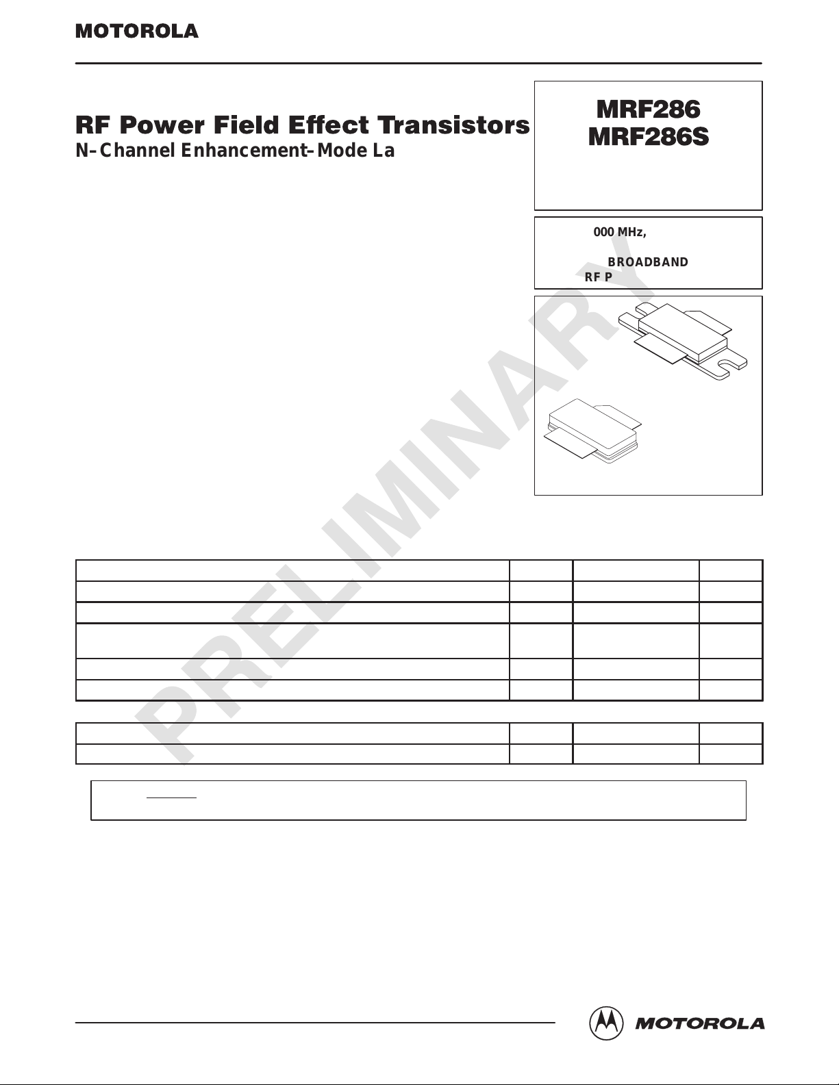
RF Power Field Effect Transistors
N–Channel Enhancement–Mode Lateral MOSFETs
Designed for PCN and PCS base station applications at frequencies from
1000 to 2400 MHz. Suitable for FM, TDMA, CDMA, and multicarrier amplifier
applications. To be used in class A and class AB for PCN–PCS/cellular radio
and WLL applications.
• Specified Two–Tone Performance @ 2000 MHz, 26 Volts
Output Power — 60 Watts (PEP)
Power Gain — 9.5 dB
Intermodulation Distortion — –28 dBc
• Typical Two–Tone Performance at 2000 MHz, 26 Volts
Output Power — 60 Watts (PEP)
Power Gain — 10.5 dB
Efficiency — 32%
Intermodulation Distortion — –30 dBc
• S–Parameter Characterization at High Bias Levels
• Capable of Handling 10:1 VSWR, @ 26 Vdc,
2000 MHz, 60 Watts (CW) Output Power
• Excellent Thermal Stability
• Characterized with Series Equivalent Large–Signal Impedance Parameters
MRF286
MRF286S
Order sample parts by XRF286,S
PILOT PRODUCTION PROTOTYPE
2000 MHz, 60 W, 26 V
LATERAL N–CHANNEL
BROADBAND
RF POWER MOSFETs
CASE 465–04, STYLE 1
(MRF286)
CASE 465A–04, STYLE 1
(MRF286S)
MAXIMUM RATINGS
Rating Symbol Value Unit
Drain–Source Voltage V
Gate–Source Voltage V
Total Device Dissipation @ TC = 25°C
Derate above 25°C
Storage Temperature Range T
Operating Junction Temperature T
THERMAL CHARACTERISTICS
Characteristic Symbol Max Unit
Thermal Resistance, Junction to Case R
NOTE – CAUTION – MOS devices are susceptible to damage from electrostatic charge. Reasonable precautions in handling and
packaging MOS devices should be observed.
“PILOT PRODUCTION PROTOTYPE (“X” Status)” devices are preproduction products and may not be released or produced in volume.
“X” status devices are for engineering evaluation and should not be used for production. Specifications are subject to change without notice.
DSS
GS
P
D
stg
J
θJC
65 Vdc
±20 Vdc
240
1.37
–65 to +150 °C
200 °C
0.73 °C/W
Watts
W/°C
REV 3
Motorola, Inc. 2000
MRF286 MRF286SMOTOROLA RF DEVICE DATA
1
Page 2
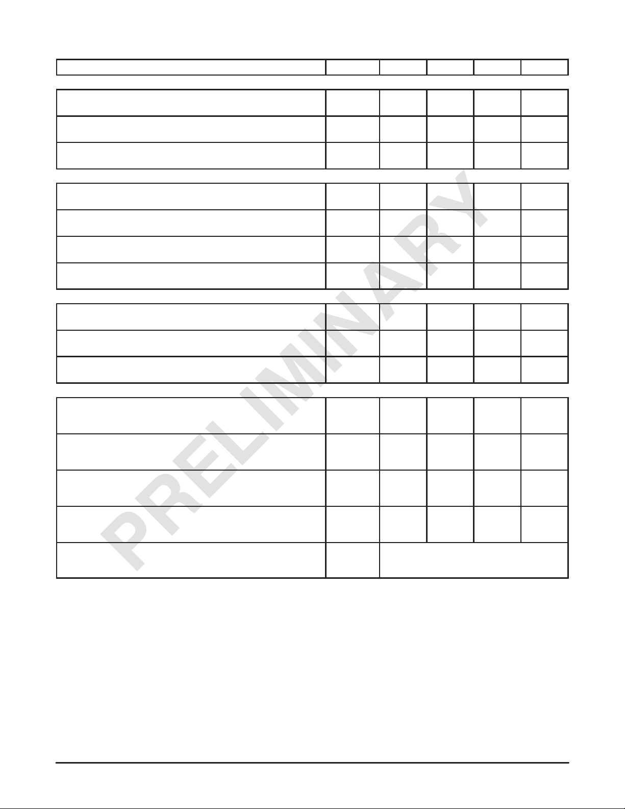
ELECTRICAL CHARACTERISTICS (T
Characteristic Symbol Min Typ Max Unit
OFF CHARACTERISTICS
Drain–Source Breakdown Voltage
(VGS = 0, ID = 20 µAdc)
Gate–Source Leakage Current
(VGS = 20 Vdc, VDS = 0 Vdc)
Zero Gate Voltage Drain Leakage Current
(VDS = 28 Vdc, VGS = 0)
ON CHARACTERISTICS
Forward Transconductance
(VDS = 10 Vdc, ID = 2 Adc)
Gate Threshold Voltage
(VDS = 10 V, ID = 300 µA)
Gate Quiescent Voltage
(VDS = 26 V, ID = 500 mA)
Drain–Source On–Voltage
(VGS = 10 V, ID = 1 A)
DYNAMIC CHARACTERISTICS
Reverse Transfer Capacitance
(VDS = 26 Vdc, VGS = 0, f = 1 MHz)
Input Capacitance
(VDS = 26 Vdc, VGS = 0, f = 1 MHz)
Output Capacitance
(VDS = 26 Vdc, VGS = 0, f = 1 MHz)
FUNCTIONAL TESTS (In Motorola Test Fixture)
Common–Source Amplifier Power Gain
(VDD = 26 Vdc, P
f1 = 2000.0 MHz, f2 = 2000.1 MHz)
Drain Efficiency
(VDD = 26 Vdc, P
f1 = 2000.0 MHz, f2 = 2000.1 MHz)
Intermodulation Distortion
(VDD = 26 Vdc, P
f1 = 2000.0 MHz, f2 = 2000.1 MHz)
Input Return Loss
(VDD = 26 Vdc, P
f1 = 2000.0 MHz, f2 = 2000.1 MHz)
Output Mismatch Stress
(VDD = 26 Vdc, P
f = 2 GHz, VSWR = 10:1, All Phase Angles at Frequency of Tests)
(1) Part is internally matched both on input and output.
(1)
= 60 W PEP, IDQ = 500 mA,
out
= 60 W PEP, IDQ = 500 mA,
out
= 60 W PEP, IDQ = 500 mA,
out
= 60 W PEP, IDQ = 500 mA,
out
= 60 W CW, IDQ = 500 mA,
out
= 25°C unless otherwise noted)
C
V
(BR)DSS
I
GSS
I
DSS
g
fs
V
GS(th)
V
GS(Q)
V
DS(on)
C
rss
C
iss
C
oss
G
ps
η 28 32 — %
IMD — 30 –28 dBc
IRL — –12 –9 dB
Ψ
65 — — Vdc
— — 1 µAdc
— — 10 µAdc
— 3 — S
2 3.2 4 Vdc
3 4.15 5 Vdc
— 0.16 0.6 Vdc
— 3 — pF
— 145 — pF
— 51 — pF
9.5 10.5 — dB
No Degradation In Output Power
MRF286 MRF286S
2
MOTOROLA RF DEVICE DATA
Page 3
T
V
R1
R2
R3
R7
R6
R5
GG
V
DD
+
C3
RF
INPUT
Z1 Z2 Z3 Z4
C1
B1
C4
C6
C2
Z1 0.436″ x 0.080″ Microstrip
Z2 0.248″ x 0.080″ Microstrip
Z3 0.610″ x 0.080″ Microstrip
Z4 0.529″ x 0.080″ Microstrip
Z5 0.024″ x 0.325″ Microstrip
Z6 0.144″ x 0.325″ Microstrip
Z7 0.098″ x 0.325″ Microstrip
Z8 0.215″ x 0.515″ Microstrip
Z9 0.215″ x 0.515″ Microstrip
Z10 0.044″ x 0.325″ Microstrip
Z11 0.060″ x 0.325″ Microstrip
Z12 0.141″ x 0.325″ Microstrip
R4
C7
Z5L1Z6 Z7
C9
C5 C8
Z8
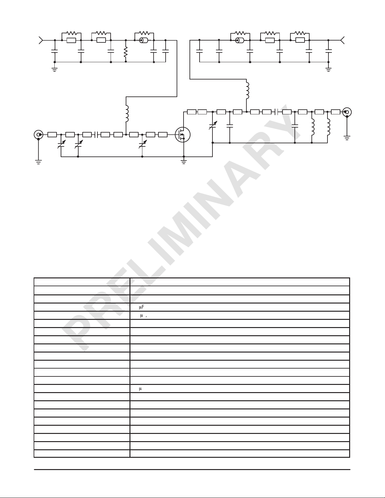
Figure 1. 1.93 – 2.0 GHz Broadband Test Circuit Schematic
DUT
B2
C15
Z9
Z10
C13 C18
Z11 Z12 Z13L3Z14
C10
C11
Z13 0.025″ x 0.325″ Microstrip
Z14 0.544″ x 0.080″ Microstrip
Z15 0.108″ x 0.080″ Microstrip
Z16 0.095″ x 0.080″ Microstrip
Z17 0.996″ x 0.080″ Microstrip
Z18 0.077″ x 0.080″ Microstrip
Board 0.030″ Glass Teflon, 2 oz Copper,
3″ x 5″ Dimensions,
RF Circuit 3″ x 5″ Copper Clad PCB,
Board Glass Teflon, εr = 2.55
C12
L2
Arlon GX0300–55–22, εr = 2.55
C14
Z15
C16
+
W4W3W2W1
Z16 Z17L4Z18
C17
+
C19
RF
OUTPU
T able 1. 1.93 – 2.0 GHz Broadband Component Designations and Values
Designators Description
B1, B2 Ferrite Bead, Round, Newark #95F769
C1, C2, C9 0.8–8.0 pF, Variable Capacitors, Gigatrim Johanson, Newark #44F3360
C3, C18
C4, C14
C5, C15 91 pF, RF Chip Capacitors, B Case, A TC #100B910JP500X
C6 8.2 pF, RF Chip Capacitor, B Case, ATC #100B8R2CP500X
C7, C12 1000 pF, RF Chip Capacitors, B Case, ATC #100B102JP50X
C8, C13 5.1 pF, RF Chip Capacitors, B Case, A TC #100B5R1CP500X
C10 0.4–2.5 pF, Variable Capacitor, Gigatrim Johanson, Newark #44F3367
C11 2.2 pF, RF Chip Capacitor, B Case, ATC #100B2R2JP500X
C16 200 pF, RF Chip Capacitor, B Case, ATC #100B201JP500X
C17 0.1 pF, RF Chip Capacitor, B Case, ATC #100B0R1BP500X
C19
L1 8 Turns, #24 AWG, 0.120″ OD, 0.270″ Long (28.0 nH), CoilCraft #B08T-5
L2 6 Turns, #24 AWG, 0.195″ OD, 0.150″ Long (47.0 nH), CoilCraft #1812SMS-47NJ
L3 2 Turns, #24 AWG, 0.120″ OD, 0.145″ Long (5.0 nH), CoilCraft #A02T-5
L4 3 Turns, #24 AWG, 0.120″ OD, 0.145″ Long (8.0 nH), CoilCraft #A03T-5
R1, R2, R3, R5, R6, R7 12 Ω, 1/4 W Chip Resistors (0.08″ x 0.13″), Garrett Instruments #RM73B2B120JT
R4 560 kΩ, 1/4 W Chip Resistor (0.08″ x 0.13″)
W1, W2, W3, W4 Solid Copper Buss Wire, #16 AWG
WS1, WS2 Beryllium Copper Wear Blocks (0.005″ x 0.210″ x 0.520″) Nominal
22 mF, 35 V Tantalum Surface Mount Chip Capacitors, Kemet #T491X226K035AS4394
0.1 mF, Chip Capacitors, Kemet #CDR33BX104AKWS
10 mF, 35 V Tantalum Surface Mount Chip Capacitor, Kemet #T495X106K035AS4394
MRF286 MRF286SMOTOROLA RF DEVICE DATA
3
Page 4
C3
C1
C2
W1
R1
C6
C5
C4
R2
W2
C7
R4
B1
R3
C8
L1
WS1
C9
C13
C11
WS2
C10
MRF286/S
Rev–0
D. W. Joersz
C12
W3
R5
R6
B2
L2
C15
C16
C14
R7
W4
L3
C17
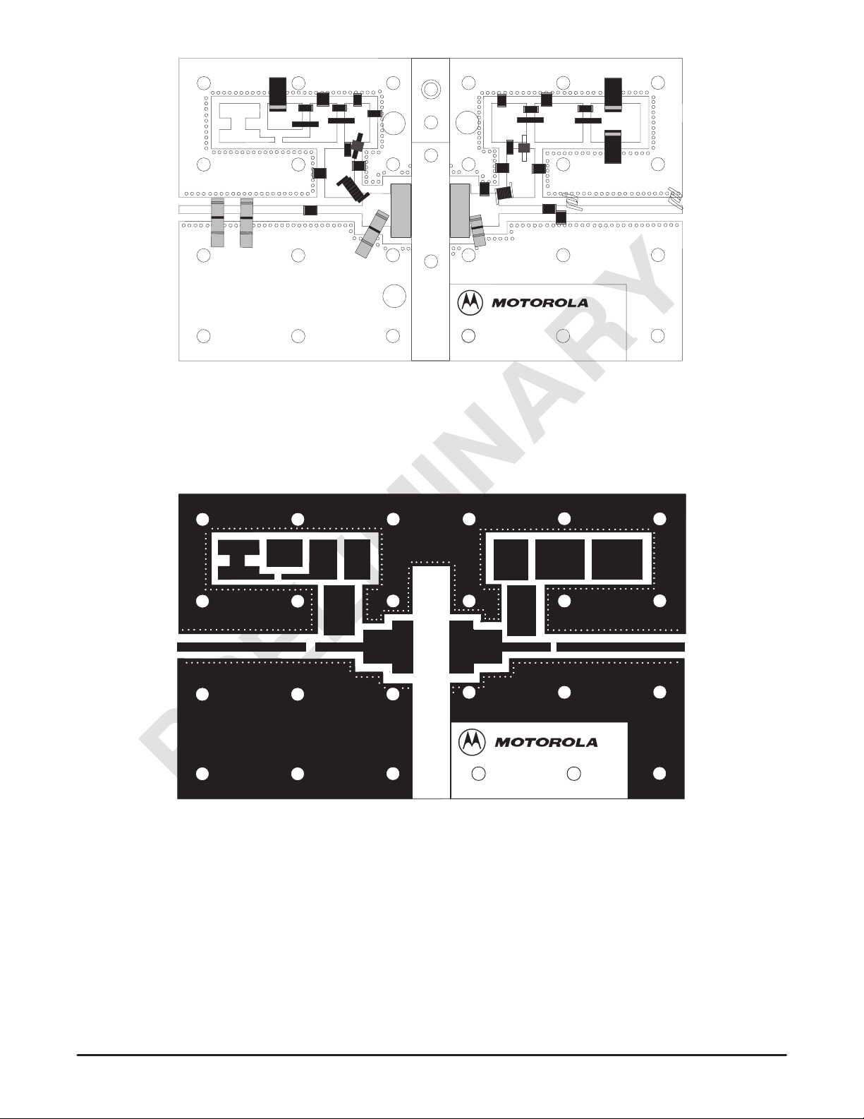
Figure 2. 1.93–2.0 GHz Broadband Test Circuit Component Layout
C18
C19
L4
MRF286 MRF286S
4
MRF286/S
Rev–0
D. W. Joersz
Figure 3. MRF286 T est Circuit Photomaster
(Reduced 18% in printed data book, DL110/D)
(Scale 1:1)
MOTOROLA RF DEVICE DATA
Page 5
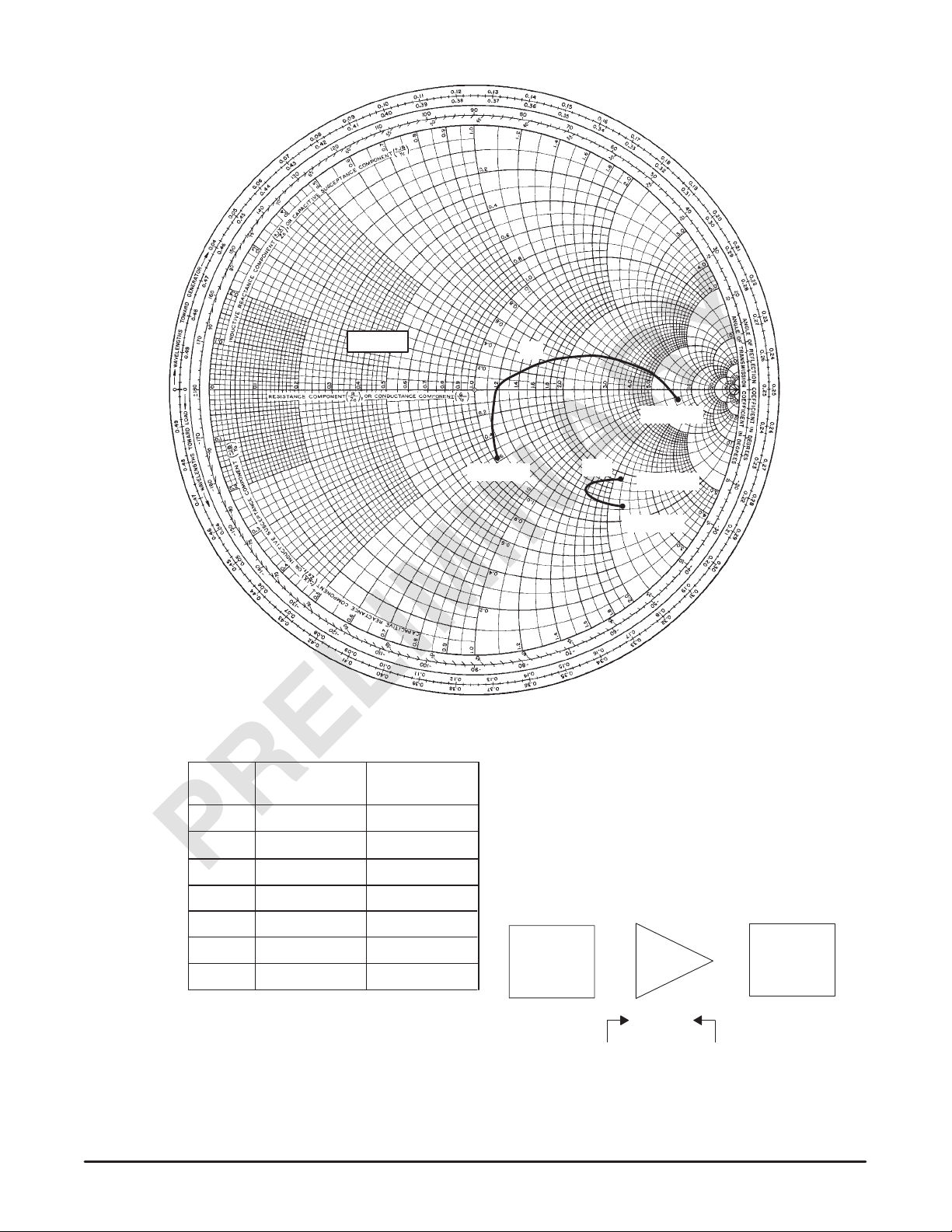
Zo = 1 Ω
Z
in
f = 2.4 GHz
VDD = 26 V, IDQ = 500 mA, P
f
MHz
1800
1900
2000
2100
2200 2.40 + j0.80 1.80 – j2.0
2300
2400
Zin= Complex conjugate of source impedance.
Z
in
Ω
1.0 – j0.57
1.19 – j0.005
1.38 + j0.20
1.75 + j0.47
4.90 + j1.20
7.50 – j1.85
= 60 Watts (PEP)
out
1.25 – j2.31
1.35 – j2.0
1.40 – j1.6
1.60 – j1.7
1.85 – j2.1
1.90 – j2.18
ZOL*
Ω
f = 1.8 GHz
Input
Matching
Network
ZOL*
f = 2.4 GHz
f = 1.8 GHz
Device
Under T est
Output
Matching
Network
ZOL* = Complex conjugate of the optimum load
impedance at given output power, voltage,
IMD, bias current and frequency.
Figure 4. Series Large–Signal Device Impedances
Z
in
ZOL*
MRF286 MRF286SMOTOROLA RF DEVICE DATA
5
Page 6
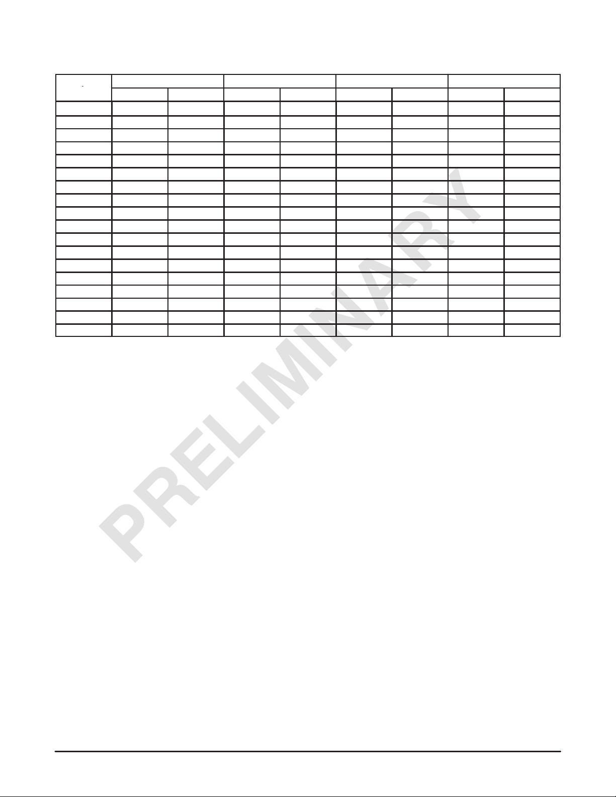
T able 2. High Bias Small–Signal S–Parameters
f
ID = 3.6 A
S
f
GHz
1.0 0.945 –180 0.458 8 0.02 105 0.905 –179
1.1 0.949 –180 0.406 5 0.02 93 0.900 –180
1.2 0.954 178 0.357 1 0.03 79 0.885 180
1.3 0.961 178 0.324 –1 0.03 73 0.874 –179
1.4 0.957 177 0.301 –3 0.03 74 0.889 –178
1.5 0.953 176 0.290 –6 0.02 59 0.899 –178
1.6 0.950 175 0.275 –9 0.02 75 0.921 –178
1.7 0.946 175 0.271 –12 0.02 79 0.927 –180
1.8 0.942 174 0.275 –16 0.03 80 0.934 180
1.9 0.936 174 0.286 –21 0.03 81 0.939 179
2.0 0.945 173 0.310 –27 0.03 83 0.943 177
2.1 0.952 171 0.354 –36 0.03 75 0.940 177
2.2 0.954 170 0.427 –51 0.04 81 0.944 176
2.3 0.915 167 0.513 –76 0.04 71 0.957 175
2.4 0.851 169 0.507 –112 0.04 72 0.970 174
2.5 0.916 172 0.417 –148 0.05 88 0.983 172
2.6 0.936 169 0.260 –180 0.08 66 0.977 170
2.7 0.953 168 0.172 164 0.08 54 0.980 170
|S11| φ |S21| φ |S12| φ |S22| φ
11
S
21
S
12
S
22
MRF286 MRF286S
MOTOROLA RF DEVICE DATA
6
Page 7
–B–
H
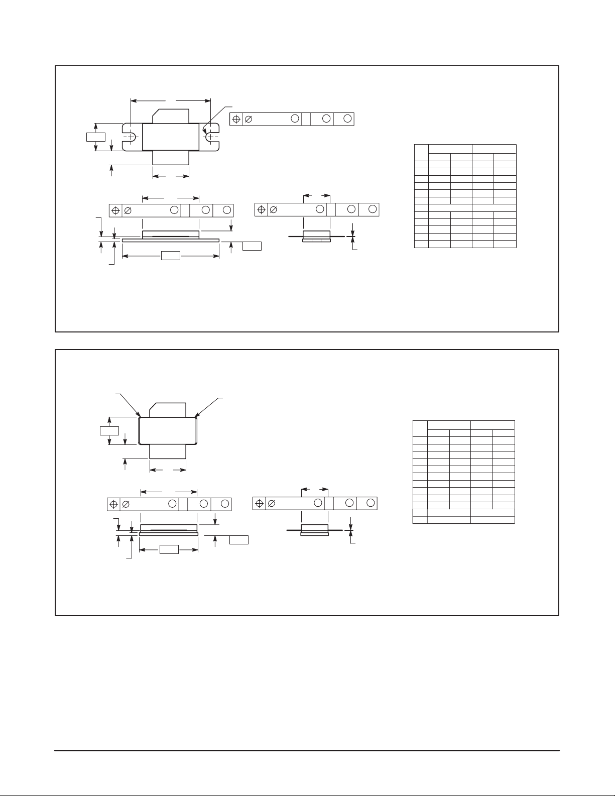
P ACKAGE DIMENSIONS
NOTES:
G
1
K
2
Q 2 PL
0.25 (0.010) B
3
M
M
A
T
M
D
N
0.38 (0.015) B
M
M
A
T
M
0.38 (0.015) B
R
M
M
A
T
M
C
–T–
E
–A–
SEATING
PLANE
F
1. DIMENSIONING AND TOLERANCING PER ANSI
Y14.5M, 1982.
2. CONTROLLING DIMENSION: INCH.
3. 465–01, –02 AND –03 OBSOLETE, NEW
STANDARD 465–04.
4. DIMENSION H IS MEASURED 0.030” AWAY FROM
FLANGE.
DIM MIN MAX MIN MAX
A 1.335 1.345 33.91 34.16
B 0.380 0.390 9.65 9.91
C 0.125 0.170 3.18 4.32
D 0.495 0.505 12.57 12.83
E 0.035 0.045 0.89 1.14
F 0.003 0.006 0.08 0.15
G 1.100 BSC 27.94 BSC
H 0.055 0.065 1.40 1.65
K 0.170 0.210 4.32 5.33
N 0.772 0.788 19.60 20.00
Q 0.118 0.138 3.00 3.51
R 0.365 0.375 9.27 9.53
STYLE 1:
PIN 1. DRAIN
2. GATE
3. SOURCE
MILLIMETERSINCHES
CASE 465–04
ISSUE D
(MRF286)
4 PL
–B–
URADIUS
K
0.64 (0.025) B
H
E
D
N
–A–
NOTES:
1. DIMENSIONING AND TOLERANCING PER ANSI
SRADIUS
1
2
4 PL
R
M
M
A
T
M
C
3
–T–
SEATING
PLANE
0.38 (0.015) B
M
M
A
T
M
F
Y14.5M, 1982.
2. CONTROLLING DIMENSION: INCH.
3. DIMENSION H IS MEASURED 0.030” AWAY FROM
FLANGE.
DIM MIN MAX MIN MAX
A 0.805 0.815 20.45 20.70
B 0.380 0.390 9.65 9.91
C 0.125 0.170 3.18 4.32
D 0.495 0.505 12.57 12.83
E 0.035 0.045 0.89 1.14
F 0.003 0.006 0.08 0.15
H 0.055 0.065 1.40 1.65
K 0.170 0.210 4.32 5.33
N 0.775 0.785 19.69 19.94
R 0.365 0.375 9.27 9.53
S 0.020 REF 0.51 REF
U 0.030 REF 0.76 REF
STYLE 1:
PIN 1. DRAIN
2. GATE
4. SOURCE
MILLIMETERSINCHES
CASE 465A–04
ISSUE D
(MRF286S)
MRF286 MRF286SMOTOROLA RF DEVICE DATA
7
Page 8

Motorola reserves the right to make changes without further notice to any products herein. Motorola makes no warranty , representation or guarantee regarding
the suitability of its products for any particular purpose, nor does Motorola assume any liability arising out of the application or use of any product or circuit, and
specifically disclaims any and all liability, including without limitation consequential or incidental damages. “T ypical” parameters which may be provided in Motorola
data sheets and/or specifications can and do vary in different applications and actual performance may vary over time. All operating parameters, including “Typicals”
must be validated for each customer application by customer’s technical experts. Motorola does not convey any license under its patent rights nor the rights of
others. Motorola products are not designed, intended, or authorized for use as components in systems intended for surgical implant into the body, or other
applications intended to support or sustain life, or for any other application in which the failure of the Motorola product could create a situation where personal injury
or death may occur. Should Buyer purchase or use Motorola products for any such unintended or unauthorized application, Buyer shall indemnify and hold Motorola
and its officers, employees, subsidiaries, affiliates, and distributors harmless against all claims, costs, damages, and expenses, and reasonable attorney fees
arising out of, directly or indirectly, any claim of personal injury or death associated with such unintended or unauthorized use, even if such claim alleges that
Motorola was negligent regarding the design or manufacture of the part. Motorola and are registered trademarks of Motorola, Inc. Motorola, Inc. is an Equal
Opportunity/Affirmative Action Employer.
How to reach us:
USA/EUROPE/Locations Not Listed: Motorola Literature Distribution; P.O. Box 5405, Denver, Colorado 80217. 1–303–675–2140 or 1–800–441–2447
JAPAN: Motorola Japan Ltd.; SPS, Technical Information Center, 3–20–1, Minami–Azabu. Minato–ku, T okyo 106–8573 Japan. 81–3–3440–3569
ASIA/PACIFIC: Motorola Semiconductors H.K. Ltd.; Silicon Harbour Centre, 2 Dai King Street, Tai Po Industrial Estate, Tai Po, N.T., Hong Ko ng. 852–26668334
Technical Information Center: 1–800–521–6274
HOME PAGE: http://www.motorola.com/semiconductors/
MRF286 MRF286S
8
MOTOROLA RF DEVICE DATA
MRF286, MRF286S PILOT PRODUCTION PROTOTYPE DATA SHEET
 Loading...