

Page 1
SEMICONDUCTOR TECHNICAL DATA
The RF MOSFET Line
RF Power
Field-Effect Transistor
N–Channel Enhancement–Mode
Designed for broadband commercial and military applications using single
ended circuits at frequencies to 500 MHz. The high power, high gain and
broadband performance of this device makes possible solid state transmitters
for FM broadcast or TV channel frequency bands.
• Guaranteed Performance @ 500 MHz, 28 Vdc
Output Power — 100 Watts
Power Gain — 8.8 dB Typ
Efficiency — 55% Typ
• 100% Ruggedness Tested At Rated Output Power
• Low Thermal Resistance
• Low C
— 17 pF Typ @ VDS = 28 Volts
rss
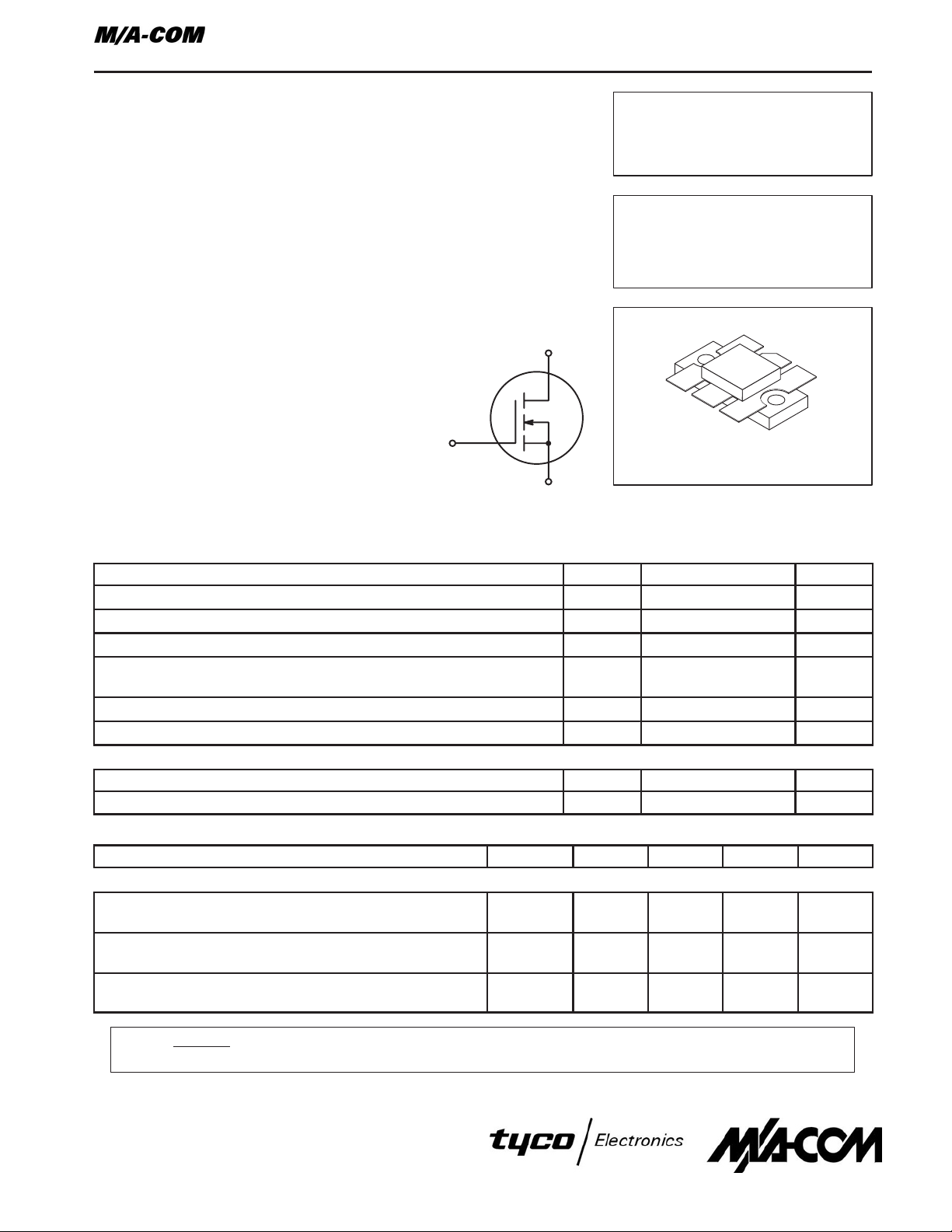
G
D
S
Order this document
by MRF275L/D
MRF275L
100 W, 28 V, 500 MHz
N–CHANNEL
BROADBAND
RF POWER FET
CASE 333–04, STYLE 2
MAXIMUM RATINGS
Rating Symbol Value Unit
Drain–Source Voltage V
Gate–Source Voltage V
Drain Current — Continuous I
Total Device Dissipation @ TC = 25°C
Derate above 25°C
Storage Temperature Range T
Operating Junction Temperature T
THERMAL CHARACTERISTICS
Characteristic Symbol Max Unit
Thermal Resistance, Junction to Case R
ELECTRICAL CHARACTERISTICS (T
Characteristic
= 25°C unless otherwise noted)
C
Symbol Min Typ Max Unit
OFF CHARACTERISTICS
Drain–Source Breakdown Voltage
(VGS = 0, ID = 50 mA)
Zero Gate Voltage Drain Current
(VDS = 28 V, VGS = 0)
Gate–Body Leakage Current
(VGS = 20 V, VDS = 0)
V
(BR)DSS
I
DSS
I
GSS
DSS
GS
D
P
D
stg
J
θJC
65 — — Vdc
— — 2.5 mAdc
— — 1.0 µAdc
65 Vdc
±20 Vdc
13 Adc
270
1.54
–65 to +150 °C
200 °C
0.65 °C/W
Watts
W/°C
NOTE – CAUTION – MOS devices are susceptible to damage from electrostatic charge. Reasonable precautions in handling and
packaging MOS devices should be observed.
REV2
1
Page 2
ELECTRICAL CHARACTERISTICS — continued (T
Characteristic Symbol Min Typ Max Unit
= 25°C unless otherwise noted)
C
ON CHARACTERISTICS
Gate Threshold Voltage (VDS = 10 V, ID = 100 mA) V
Drain–Source On–Voltage (VGS = 10 V, ID = 5.0 A) V
Forward Transconductance (VDS = 10 V, ID = 2.5 A) g
DYNAMIC CHARACTERISTICS
Input Capacitance (VDS = 28 V, VGS = 0, f = 1.0 MHz) C
Output Capacitance (VDS = 28 V, VGS = 0, f = 1.0 MHz) C
Reverse Transfer Capacitance (VDS = 28 V, VGS = 0, f = 1.0 MHz) C
FUNCTIONAL CHARACTERISTICS
Common Source Power Gain
(VDD = 28 Vdc, P
Drain Efficiency
(VDD = 28 Vdc, P
Electrical Ruggedness
(VDD = 28 Vdc, P
VSWR 10:1 at all Phase Angles)
= 100 W, f = 500 MHz, IDQ = 100 mA)
out
= 100 W, f = 500 MHz, IDQ = 100 mA)
out
= 100 W, f = 500 MHz, IDQ = 100 mA,
out
GS(th)
DS(on)
fs
iss
oss
rss
G
ps
η 50 55 — %
ψ
1.5 2.5 4.5 Vdc
0.5 0.9 1.5 Vdc
3.0 3.75 — mhos
— 135 — pF
— 140 — pF
— 17 — pF
7.5 8.8 — dB
No Degradation in Output Power
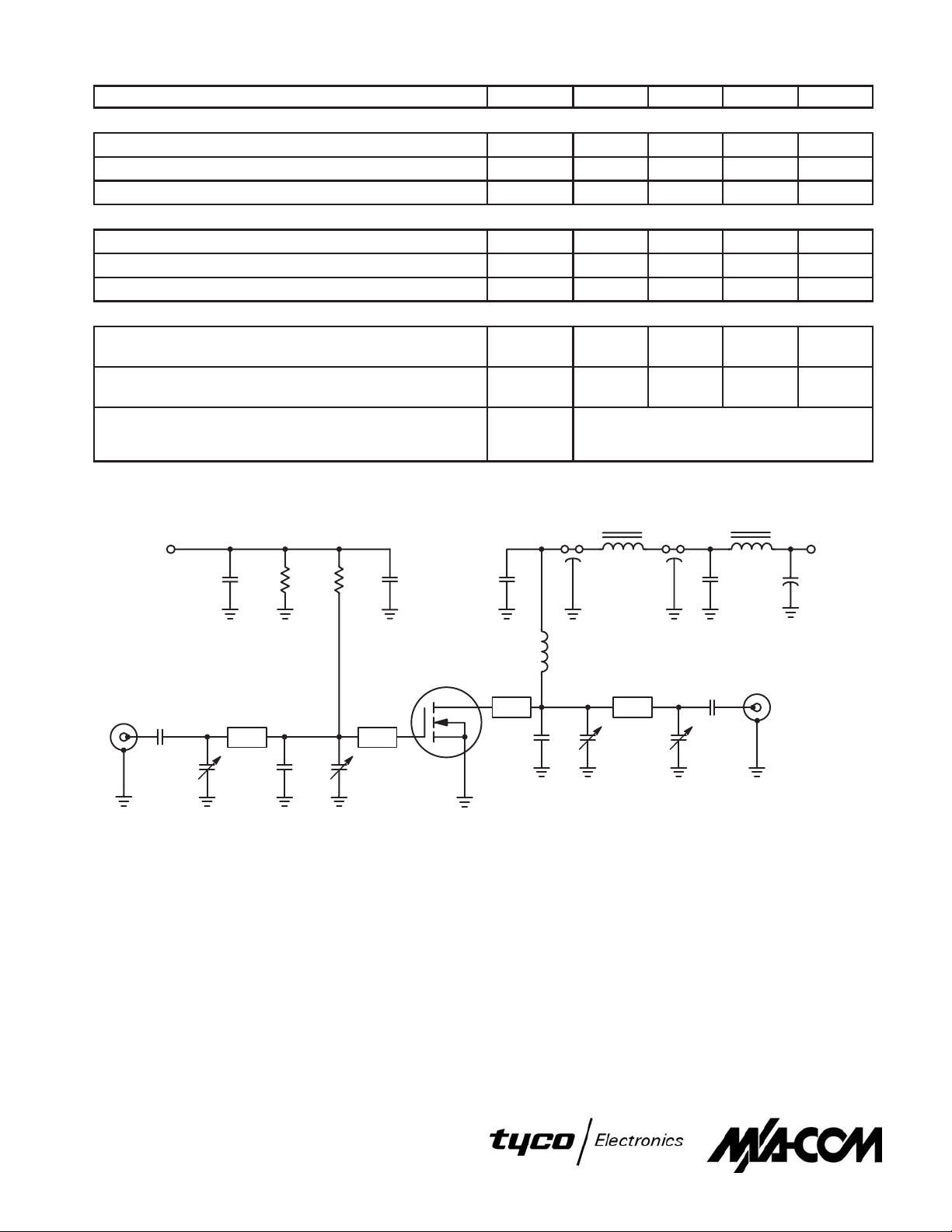
+V
GG
C1
RF
INPUT
C3
C1, C11, C14 0.1 µF, Ceramic Capacitor
C2 240 pF, ATC Type Chip Capacitor
C3, C10 270 pF, ATC Type Chip Capacitor
C4, C6, C8, C9 1–20 pF, Trimmer Capacitor, Johansen
C5 24 pF, Mini–Unelco Type Capacitor
C7 24 pF, Mini–Unelco Type Capacitor
C12, C13 680 pF, Feedthru Capacitors
C15 10 µF, 50 V, Electrolytic Capacitor
R1
Z1
R2
C2
Z2
C6C5C4
DUT
C12 C13
RFC2
C11
RFC1
Z3
C7 C8
RFC1 8 Turns AWG #18, 0.25″I.D., Enameled
RFC2, RFC3 Ferroxcube VK200 19/4B
Z1, 0.250″ x 0.800″, Microstrip Line
Z2, Z3 0.250″ x 0.400″,Microstrip Line
Z4 0.250″ x 1.25″, Microstrip Line
Board Material 0.062″ Glass Teflon,
Z4
C9
2 oz. Copper, Double Clad Copper
Board, εr = 2.55
C10
RFC3
C14
RF
OUTPUT
+
+28 V
C15
REV2
2
Figure 1. 500 MHz Test Circuit
Page 3
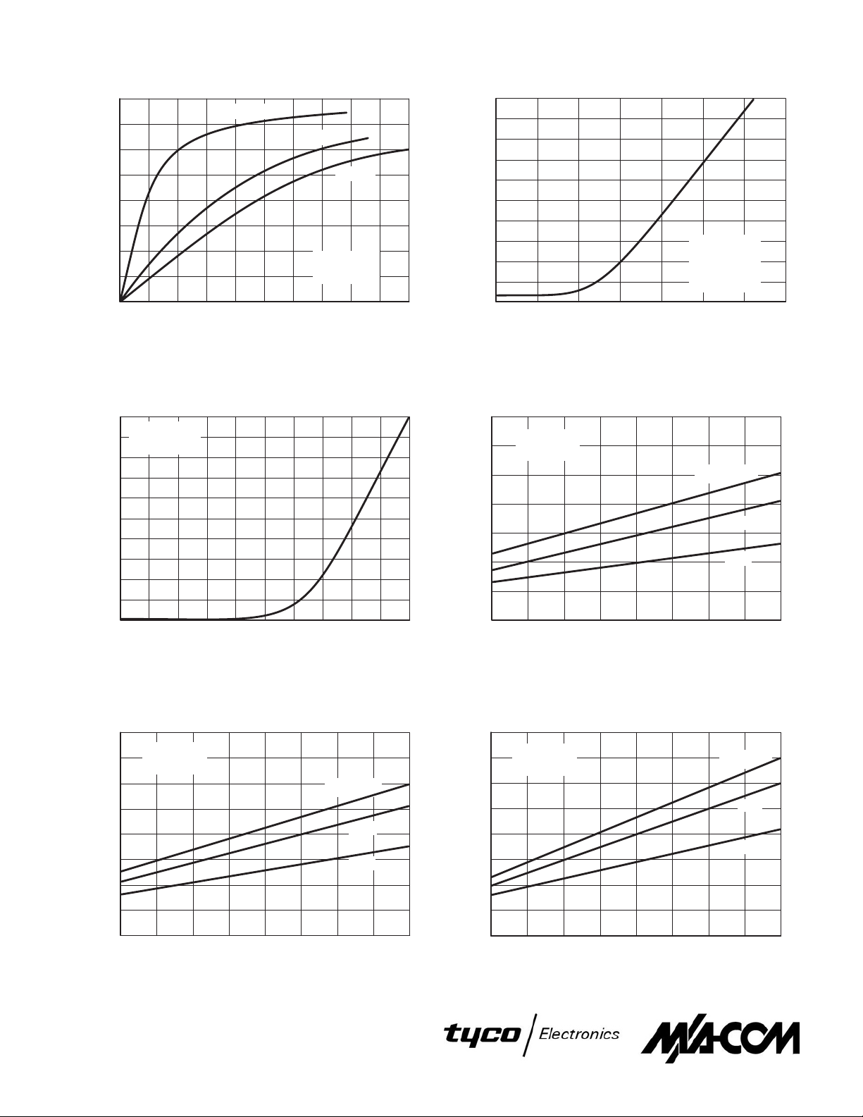
TYPICAL CHARACTERISTICS
160
140
120
100
, OUTPUT POWER (WATTS)
out
P
80
60
40
20
0
412
f = 225 MHz
8
10614218
Pin, INPUT POWER (WA TTS)
Figure 2. Output Power versus Input Power
10
VDS = 10 V
9
V
= 2.5 V
GS(th)
8
7
6
5
4
3
, DRAIN CURRENT (AMPS)
D
I
2
1
0
0
VGS, GATE–SOURCE VOLTAGE (VOLTS)
2
315
400 MHz
VDD = 28 V
IDQ = 100 mA
500 MHz
16
4
100
90
80
70
60
50
40
30
, OUTPUT POWER (WATTS)
out
20
P
10
0
20
–10 00
–6 –4
–8
VGS, GATE–SOURCE VOLTAGE (VOLTS)
–2
VDS = 28 V
IDQ = 100 mA
Pin = Constant
f = 500 MHz
42
Figure 3. Output Power versus Gate Voltage
140
0
IDQ = 100 mA
f = 500 MHz
14 1612
18 20 28
VDD, SUPPLY VOLTAGE (VOLTS)
Pin = 13.5 W
10 W
6 W
24
22 26
120
100
80
60
, OUTPUT POWER (WATTS)
40
out
P
20
4.52.50.5 3.51.5
Figure 4. Drain Current versus Gate Voltage
(Transfer Characteristics)
160
80
60
40
20
IDQ = 100 mA
f = 400 MHz
0
14 1612 18 20 282422 26
VDD, SUPPLY VOLTAGE (VOLTS)
140
120
100
, OUTPUT POWER (WATTS)
out
P
Figure 6. Output Power versus Supply Voltage
REV2
3
Pin = 14 W
10 W
6 W
Figure 5. Output Power versus Supply Voltage
160
80
60
40
20
IDQ = 100 mA
f = 225 MHz
0
14 1612 18 20 282422 26
VDD, SUPPLY VOLTAGE (VOLTS)
, OUTPUT POWER (WATTS)
out
P
140
120
100
Figure 7. Output Power versus Supply Voltage
Pin = 8 W
4 W
2 W
Page 4
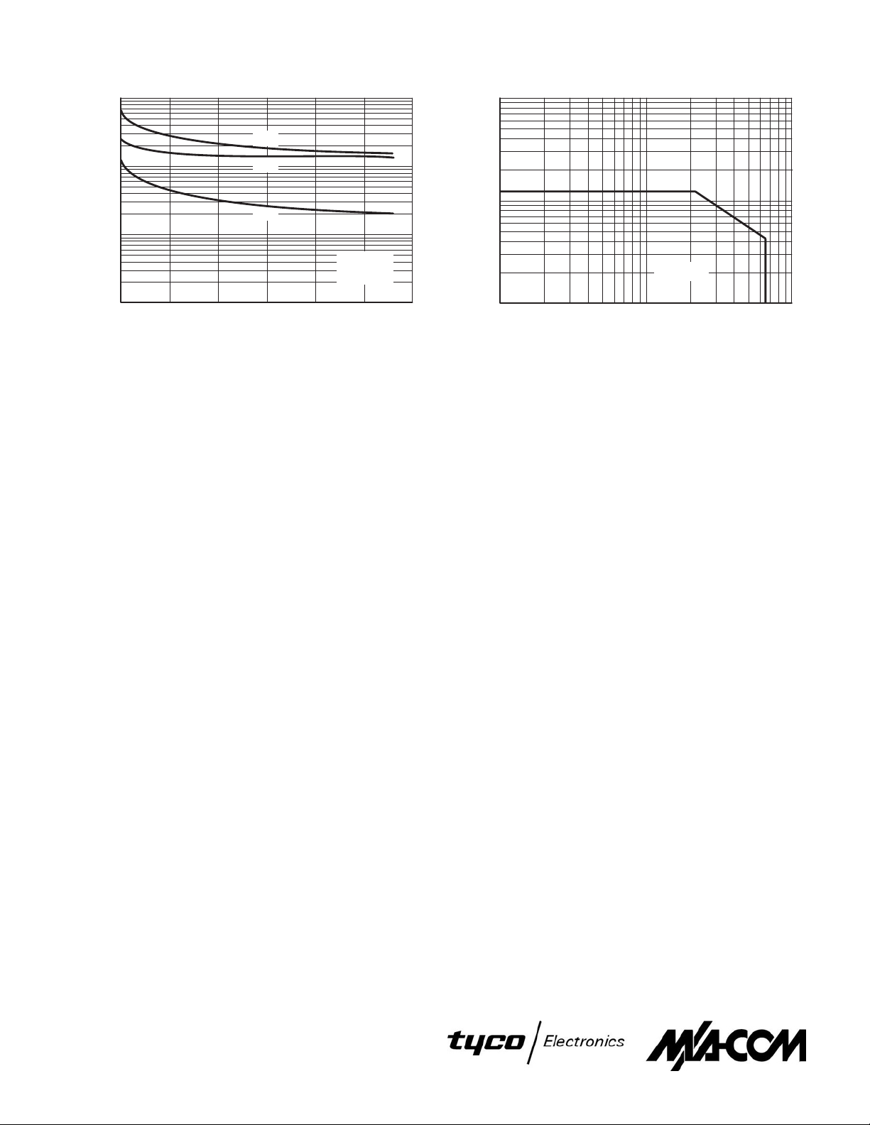
TYPICAL CHARACTERISTICS
1000
C
oss
C, CAPACITANCE (pF)
100
10
1
0
515
10
VDS, DRAIN–SOURCE VOLTAGE (VOLTS)
C
iss
C
rss
VGS = 0 V
f = 1.0 MHz
20 1 10025
Figure 8. Capacitance versus Drain–Source V oltage
100
10
, DRAIN CURRENT (AMPS)
D
I
TC = 25°C
30
1
VDS, DRAIN–SOURCE VOLTAGE (VOLTS)
10
Figure 9. DC Safe Operating Area
REV2
4
Page 5

f = 500 MHz
400
225
f = 500 MHz
Z
Zo = 10 Ω
in
400
225
ZOL*
Zo = 10 Ω
VDD = 28 V, IDQ = 100 mA, P
f
(MHz)
225
400
500
ZOL* = Conjugate of the optimum load impedance into which the device
Z
Ohms
1.1 – j1.7
1.08 – j1.5
1.0 – j0.5
operates at a given output power, voltage and frequency.
Figure 10. Series Equivalent Input/Output Impedance
in
out
= 100 W
VDD = 28 V, IDQ = 100 mA, P
f
(MHz)
225
400
500
ZOL*
Ohms
1.6 – j1.3
0.9 – j0.5
1.0 – j0.2
= 100 W
out
REV2
5
Page 6

BIAS
RF INPUT
R1
C1
C4
RFC1
C5 C10 C11
R2
L1
L4
L3L2
+
C9
+28 Vdc
RF OUTPUT
C2 C3 C6 C7
C1, C2, C8 Arco 463 or Equivalent
C3, C7 25 pF, Unelco Capacitor
C4 1000 pF, Chip Capacitor
C5 0.01 µF, Chip Capacitor
C6 250 pF, Unelco Capacitor
C9 Arco 462 or Equivalent
C10 1000 pF, ATC Chip Capacitor
C11 10 µF, 100 V, Electrolytic Capacitor
BIAS
RF
INPUT
C9
.01 mf
C1
R2
R1
L1
Z1
DUT
L1 Hairpin Inductor #18 Wire
0.32″
0.15″
L2 Stripline Inductor 0.200″ x 0.500″
Figure 11. 225 MHz Test Circuit
C12
C11 C13
L2
C8
L3 Hairpin Inductor #16 Wire
0.45″
0.2″
L4 2 Turns #16 Wire, 5/16″ ID
RFC1 VK200–4B
R1 1.0 k, 1/4 W Resistor
R2 100 Ω Resistor
L3
Z2
C14
C8
Z3
+ v
GND
RF
OUTPUT
C2
C1, C8 270 pF, ATC Chip Capacitor
C2, C4, C6, C7 1.0–20 pF, Trimmer Capacitor
C3 15 pF, Mini Unelco Capacitor
C5 47 pF, Mini Unelco Capacitor
C9, C12 0.1 µF, Ceramic Capacitor
C11, C14 680 pF , Feed Thru Capacitor
C13 50 µF, Tantalum Capacitor
REV2
C3
6
C4
DUT
L1 Hairpin Inductor #18 Wire
0.25″
0.4″
L2 12 Turns #18 Wire, 0.450″ ID
L3 Ferroxcube VK200 20/4B
Figure 12. 400 MHz T est Circuit
C7C6C5
R1 10 k, 1/4 W Resistor
R2 1 k, 1/4 W Resistor
R3 1.5 k, 1/4 W Resistor
Z1 0.950″ x 0.250″, Microstrip Line
Z2 1.25″ x 0.250″, Microstrip Line
Z3 0.300″ x 0.250″, Microstrip Line
Board Material 0.062″ Teflon,
Fiberglass, 1 oz. Copper,
Clad Both Sides, εr = 2.56
Page 7

+
C3
RFC2
C12 C13
BEADS
C11 C14
RFC1
C4
C1
R1
C2
R2
C5 C7
C6 C8 C9
Figure 13. MRF275L Component Location (500 MHz)
RFC3
C15
+
C10
(Not to Scale)
+
REV2
7
MRF275L
(Scale 1:1)
Figure 14. MRF275L T est Circuit Photomaster
(Reduced 18% in printed data book, DL110/D)
Page 8

T able 1. Common Source S–Parameters (VDS = 12.5 V, ID = 4.5 A)
f
S
11
MHz
30 0.936 –176 6.22 87 0.010 21 0.944 –179
40 0.938 –178 4.28 87 0.010 24 0.930 –177
50 0.937 –178 3.65 83 0.010 29 0.922 179
60 0.937 –179 2.99 83 0.011 34 0.920 179
70 0.938 –179 2.54 81 0.011 39 0.917 179
80 0.938 –179 2.18 80 0.012 42 0.913 179
90 0.939 –180 1.94 78 0.012 44 0.909 180
100 0.939 –180 1.77 77 0.013 47 0.913 –180
110 0.939 180 1.57 77 0.015 50 0.916 –179
120 0.940 180 1.45 74 0.015 54 0.914 179
130 0.940 179 1.34 75 0.016 57 0.935 180
140 0.940 179 1.26 72 0.016 58 0.943 180
150 0.940 179 1.19 71 0.017 57 0.951 178
160 0.941 179 1.09 70 0.019 58 0.943 179
170 0.941 179 1.01 69 0.019 62 0.940 180
180 0.941 179 0.956 68 0.021 64 0.948 179
190 0.941 178 0.912 67 0.022 65 0.957 180
200 0.942 178 0.860 65 0.022 65 0.941 178
210 0.942 178 0.816 64 0.023 65 0.931 178
220 0.943 178 0.779 63 0.025 66 0.922 178
230 0.943 177 0.717 60 0.027 67 0.965 177
240 0.943 177 0.709 61 0.026 68 0.927 176
250 0.944 177 0.674 60 0.026 70 0.924 178
260 0.944 177 0.645 58 0.028 69 0.930 179
270 0.944 177 0.627 57 0.030 70 0.933 178
280 0.945 176 0.608 58 0.032 70 0.940 177
290 0.946 176 0.580 54 0.031 71 0.941 175
300 0.946 176 0.569 56 0.033 71 0.945 176
310 0.946 176 0.539 55 0.033 72 0.953 178
320 0.947 175 0.512 54 0.035 71 0.952 177
330 0.948 175 0.483 51 0.037 72 0.927 176
340 0.947 175 0.477 52 0.038 72 0.921 176
350 0.947 175 0.466 51 0.039 75 0.929 178
360 0.947 175 0.459 51 0.040 73 0.963 177
370 0.948 174 0.441 50 0.043 71 0.968 175
380 0.949 174 0.428 49 0.044 72 0.937 175
390 0.949 174 0.417 49 0.045 74 0.907 176
400 0.949 174 0.409 47 0.044 77 0.912 177
410 0.950 173 0.390 46 0.046 74 0.962 175
420 0.950 173 0.377 45 0.047 71 0.971 174
430 0.950 173 0.369 45 0.050 72 0.948 176
440 0.951 173 0.368 47 0.052 74 0.953 176
|S11| φ |S21| φ |S12| φ |S22| φ
S
21
S
12
S
22
REV2
8
Page 9

T able 1. Common Source S–Parameters (VDS = 12.5 V, ID = 4.5 A) (continued)
f
S
f
f
MHz
MHz
450 0.951 172 0.371 42 0.053 76 0.943 175
460 0.952 172 0.347 44 0.053 72 0.965 172
470 0.952 172 0.331 43 0.053 71 0.933 173
480 0.953 172 0.323 43 0.056 71 0.936 173
490 0.953 171 0.317 41 0.059 72 0.965 173
500 0.954 171 0.306 41 0.061 74 0.963 173
600 0.957 168 0.267 35 0.069 77 0.941 171
700 0.965 165 0.224 35 0.090 70 0.958 169
800 0.967 160 0.219 32 0.099 67 0.937 164
900 0.980 156 0.214 33 0.114 69 0.943 164
1000 0.986 151 0.218 34 0.146 67 0.955 162
11
S
21
S
12
S
22
T able 2. Common Source S–Parameters (VDS = 24 V, ID = 4.5 A)
S
11
MHz
30 0.914 –174 9.08 87 0.011 19 0.882 –178
40 0.918 –176 6.29 86 0.011 22 0.876 –176
50 0.918 –177 5.31 82 0.011 26 0.871 180
60 0.917 –177 4.35 82 0.012 29 0.871 –179
70 0.919 –178 3.70 79 0.012 32 0.865 –179
80 0.919 –178 3.16 77 0.013 37 0.857 –179
90 0.920 –179 2.81 75 0.013 42 0.851 –180
100 0.921 –179 2.55 74 0.014 46 0.863 –179
110 0.922 –179 2.27 73 0.014 47 0.876 –178
120 0.923 –179 2.08 70 0.015 49 0.867 –179
130 0.923 –180 1.92 70 0.016 51 0.880 –178
140 0.924 –180 1.78 67 0.017 55 0.880 –179
150 0.925 –180 1.68 65 0.018 58 0.904 179
160 0.926 180 1.53 64 0.018 60 0.901 –180
170 0.927 180 1.42 62 0.018 61 0.900 –179
180 0.928 180 1.34 62 0.020 61 0.901 –179
190 0.929 179 1.28 60 0.021 63 0.906 –179
200 0.930 179 1.19 58 0.022 65 0.892 179
210 0.931 179 1.12 56 0.022 67 0.902 178
220 0.932 179 1.06 55 0.023 68 0.903 179
230 0.933 179 0.988 53 0.024 67 0.931 179
240 0.934 178 0.960 53 0.025 69 0.889 179
250 0.934 178 0.910 52 0.026 73 0.877 180
260 0.935 178 0.866 50 0.026 74 0.895 180
270 0.936 178 0.838 49 0.027 74 0.908 180
280 0.937 177 0.803 49 0.029 71 0.923 179
290 0.939 177 0.766 46 0.030 72 0.915 177
|S11| φ |S21| φ |S12| φ |S22| φ
S
21
S
12
S
22
φ|S22|φ|S12|φ|S21|φ|S11|
REV2
9
Page 10

T able 2. Common Source S–Parameters (VDS = 24 V, ID = 4.5 A) (continued)
f
S
f
f
MHz
MHz
300 0.939 177 0.744 46 0.032 76 0.907 178
310 0.939 177 0.702 46 0.032 81 0.908 180
320 0.940 176 0.660 45 0.031 81 0.913 178
330 0.941 176 0.623 41 0.031 75 0.909 177
340 0.942 176 0.613 42 0.035 71 0.910 178
350 0.943 176 0.599 41 0.039 78 0.905 –180
360 0.943 175 0.585 41 0.040 83 0.913 179
370 0.943 175 0.556 39 0.037 85 0.924 176
380 0.944 175 0.534 38 0.035 80 0.922 175
390 0.944 175 0.512 38 0.037 73 0.907 176
400 0.946 174 0.503 37 0.043 76 0.906 179
410 0.948 174 0.482 36 0.049 81 0.944 177
420 0.948 174 0.464 35 0.047 87 0.940 176
430 0.947 174 0.450 36 0.040 88 0.912 176
440 0.947 173 0.440 36 0.039 79 0.947 176
450 0.948 173 0.445 32 0.047 73 0.944 177
460 0.951 173 0.414 32 0.057 75 0.959 174
470 0.952 173 0.397 32 0.057 86 0.913 176
480 0.951 172 0.387 33 0.050 95 0.908 175
490 0.950 172 0.376 31 0.042 90 0.941 174
500 0.950 172 0.361 31 0.044 74 0.963 175
600 0.957 168 0.287 24 0.073 75 0.932 172
700 0.965 164 0.231 24 0.091 70 0.952 169
800 0.966 160 0.216 23 0.091 67 0.928 163
900 0.979 156 0.205 27 0.112 69 0.930 164
1000 0.981 150 0.206 29 0.146 58 0.947 162
11
S
21
S
12
S
22
φ|S22|φ|S12|φ|S21|φ|S11|
T able 3. Common Source S–Parameters (VDS = 28 V, ID = 4.5 A)
S
11
MHz
30 0.910 –173 9.76 87 0.011 17 0.872 –177
40 0.913 –175 6.73 86 0.011 17 0.860 –174
50 0.913 –176 5.69 81 0.011 21 0.849 –179
60 0.913 –177 4.66 81 0.012 26 0.846 –178
70 0.915 –177 3.97 78 0.012 31 0.853 –179
80 0.916 –178 3.39 76 0.012 33 0.858 –178
90 0.916 –178 3.01 74 0.012 34 0.853 –178
100 0.917 –178 2.73 73 0.013 36 0.851 –177
110 0.918 –179 2.42 72 0.014 41 0.849 –177
120 0.919 –179 2.22 68 0.014 48 0.853 –178
130 0.920 –179 2.05 68 0.014 52 0.879 –178
140 0.921 –179 1.90 66 0.014 52 0.894 –178
150 0.922 –180 1.79 64 0.015 51 0.898 –178
REV2
10
|S11| φ |S21| φ |S12| φ |S22| φ
S
21
S
12
S
22
Page 11

T able 3. Common Source S–Parameters (VDS = 28 V, ID = 4.5 A) (continued)
S
f
f
MHz
MHz
160 0.923 –180 1.63 63 0.016 53 0.880 –177
170 0.924 –180 1.50 61 0.017 58 0.890 –178
180 0.925 180 1.42 60 0.019 62 0.904 –178
190 0.926 180 1.35 58 0.019 64 0.922 –179
200 0.928 179 1.26 56 0.019 63 0.914 –179
210 0.929 179 1.19 54 0.020 62 0.897 –179
220 0.930 179 1.12 53 0.022 64 0.881 –179
230 0.932 179 1.04 51 0.024 67 0.907 180
240 0.932 179 1.01 51 0.024 69 0.892 179
250 0.933 178 0.955 49 0.024 70 0.910 –180
260 0.934 178 0.912 47 0.025 70 0.912 –178
270 0.936 178 0.882 46 0.027 71 0.904 –178
280 0.936 178 0.842 46 0.029 72 0.901 –180
290 0.938 177 0.798 43 0.028 71 0.920 177
300 0.939 177 0.770 44 0.030 71 0.930 178
310 0.939 177 0.731 43 0.032 72 0.934 –179
320 0.941 177 0.690 42 0.035 74 0.939 –180
330 0.942 176 0.655 39 0.036 76 0.895 180
340 0.942 176 0.639 40 0.035 75 0.892 179
350 0.942 176 0.613 39 0.036 75 0.906 –180
360 0.943 175 0.601 38 0.040 71 0.945 179
370 0.945 175 0.577 36 0.045 71 0.960 178
380 0.946 175 0.555 35 0.047 74 0.928 178
390 0.947 175 0.531 35 0.045 79 0.893 178
400 0.946 174 0.518 34 0.042 80 0.892 179
410 0.947 174 0.492 33 0.044 72 0.948 176
420 0.948 174 0.472 32 0.049 67 0.960 176
430 0.950 173 0.462 32 0.056 71 0.936 179
440 0.951 173 0.455 32 0.058 78 0.945 179
450 0.951 173 0.460 30 0.054 82 0.920 177
460 0.950 173 0.424 30 0.050 73 0.951 173
470 0.950 172 0.400 29 0.053 65 0.937 174
480 0.952 172 0.389 29 0.063 65 0.941 175
490 0.954 172 0.382 27 0.071 72 0.960 175
500 0.955 172 0.367 27 0.069 80 0.954 176
600 0.958 168 0.284 22 0.071 80 0.935 172
700 0.967 164 0.226 22 0.088 71 0.950 169
800 0.967 160 0.211 22 0.096 67 0.929 164
900 0.979 156 0.197 26 0.116 69 0.929 165
1000 0.978 150 0.200 29 0.139 67 0.944 163
11
S
21
S
12
S
22
φ|S22|φ|S12|φ|S21|φ|S11|
REV2
11
Page 12

RF POWER MOSFET CONSIDERA TIONS
MOSFET CAPACITANCES
The physical structure of a MOSFET results in capacitors
between the terminals. The metal oxide gate structure determines the capacitors from gate–to–drain (Cgd), and gate–to–
source (Cgs). The PN junction formed during the fabrication
of the FET results in a junction capacitance from drain–to–
source (Cds).
These capacitances are characterized as input (C
put (C
) and reverse transfer (C
oss
) capacitances on data
rss
iss
), out-
sheets. The relationships between the inter–terminal capacitances and those given on data sheets are shown below. The
C
can be specified in two ways:
iss
1. Drain shorted to source and positive voltage at the gate.
2. Positive voltage of the drain in respect to source and zero
volts at the gate. In the latter case the numbers are lower.
However, neither method represents the actual operating conditions in RF applications.
DRAIN
C
ds
SOURCE
C
iss
C
oss
C
rss
= Cgd + C
= Cgd + C
= C
gd
gs
ds
GATE
C
gd
C
gs
DRAIN CHARACTERISTICS
One figure of merit for a FET is its static resistance in the
full–on condition. This on–resistance, V
DS(on)
, occurs in the
linear region of the output characteristic and is specified under specific test conditions for gate–source voltage and drain
current. For MOSFETs, V
has a positive temperature
DS(on)
coefficient and constitutes an important design consideration
at high temperatures, because it contributes to the power
dissipation within the device.
GATE CHARACTERISTICS
The gate of the FET is a polysilicon material, and is electrically isolated from the source by a layer of oxide. The input
resistance is very high — on the order of 109 ohms — resulting in a leakage current of a few nanoamperes.
Gate control is achieved by applying a positive voltage
slightly in excess of the gate–to–source threshold voltage,
V
GS(th)
.
Gate Voltage Rating — Never exceed the gate voltage
rating. Exceeding the rated VGS can result in permanent
damage to the oxide layer in the gate region.
Gate Termination — The gates of these devices are
essentially capacitors. Circuits that leave the gate open–circuited or floating should be avoided. These conditions can
result in turn–on of the devices due to voltage build–up on
the input capacitor due to leakage currents or pickup.
Gate Protection — These devices do not have an internal
monolithic zener diode from gate–to–source. If gate protection is required, an external zener diode is recommended.
Using a resistor to keep the gate–to–source impedance
low also helps damp transients and serves another important
function. Voltage transients on the drain can be coupled to
the gate through the parasitic gate–drain capacitance. If the
gate–to–source impedance and the rate of voltage change
on the drain are both high, then the signal coupled to the gate
may be large enough to exceed the gate–threshold voltage
and turn the device on.
HANDLING CONSIDERATIONS
When shipping, the devices should be transported only in
antistatic bags or conductive foam. Upon removal from the
packaging, careful handling procedures should be adhered
to. Those handling the devices should wear grounding straps
and devices not in the antistatic packaging should be kept in
metal tote bins. MOSFETs should be handled by the case
and not by the leads, and when testing the device, all leads
should make good electrical contact before voltage is applied. As a final note, when placing the FET into the system it
is designed for, soldering should be done with a grounded
iron.
DESIGN CONSIDERATIONS
The MRF275L is a RF power N–channel enhancement
mode field–effect transistor (FETs) designed for HF, VHF and
UHF power amplifier applications. M/A-COM FETs feature a
vertical structure with a planar design.
M/A-COM Application Note AN211A, FETs in Theory and
Practice, is suggested reading for those not familiar with the
construction and characteristics of FETs.
The major advantages of RF power FETs include high
gain, low noise, simple bias systems, relative immunity from
thermal runaway, and the ability to withstand severely mismatched loads without suffering damage. Power output can
be varied over a wide range with a low power dc control signal.
DC BIAS
The MRF275L is an enhancement mode FET and, therefore, does not conduct when drain voltage is applied. Drain
current flows when a positive voltage is applied to the gate.
RF power FETs require forward bias for optimum performance. The value of quiescent drain current (IDQ) is not critical for many applications. The MRF275L was characterized
at IDQ = 100 mA, each side, which is the suggested minimum
value of IDQ. For special applications such as linear amplification, IDQ may have to be selected to optimize the critical
parameters.
The gate is a dc open circuit and draws no current. Therefore, the gate bias circuit may be just a simple resistive divider network. Some applications may require a more elaborate
bias system.
GAIN CONTROL
Power output of the MRF275L may be controlled from its
rated value down to zero (negative gain) by varying the dc
gate voltage. This feature facilitates the design of manual
gain control, AGC/ALC and modulation systems.
REV2
12
Page 13

P ACKAGE DIMENSIONS
–A–
L
D
2
1
3
P
4
K
–B–
K
Q 2 PL
M
0.13 (0.005) B
A
T
M
M
F
G
J
H
N
E
C
SEATING
–T–
PLANE
NOTES:
1. DIMENSIONING AND TOLERANCING PER ANSI
Y14.5M, 1982.
2. CONTROLLING DIMENSION: INCH.
DIM MIN MAX MIN MAX
A 0.965 0.985 24.51 25.02
B 0.390 0.410 9.91 10.41
C 0.250 0.290 6.73 7.36
D 0.190 0.210 4.83 5.33
E 0.095 0.115 2.42 2.92
F 0.215 0.235 5.47 5.96
G 0.725 BSC 18.42 BSC
H 0.155 0.175 3.94 4.44
J 0.004 0.006 0.10 0.15
K 0.195 0.205 4.95 5.21
L 0.740 0.770 18.80 19.55
N 0.415 0.425 10.54 10.80
P 0.390 0.400 9.91 10.16
Q 0.120 0.135 3.05 3.42
STYLE 2:
PIN 1. SOURCE
2. DRAIN
3. SOURCE
4. GATE
MILLIMETERSINCHES
CASE 333–04
ISSUE E
Specifications subject to change without notice.
n
North America: Tel. (800) 366-2266, Fax (800) 618-8883
n Asia/Pacific: Tel.+81-44-844-8296, Fax +81-44-844-8298
n
Europe: Tel. +44 (1344) 869 595, Fax+44 (1344) 300 020
Visit www.macom.com for additional data sheets and product information.
REV2
13
 Loading...