

Page 1
SEMICONDUCTOR TECHNICAL DATA
The RF MOSFET Line
Order this document
by MRF275G/D
Power Field-Effect Transistor
N–Channel Enhancement–Mode
Designed primarily for wideband large–signal output and driver stages from
100 – 500 MHz.
• Guaranteed Performance @ 500 MHz, 28 Vdc
Output Power — 150 Watts
Power Gain — 10 dB (Min)
Efficiency — 50% (Min)
100% Tested for Load Mismatch at all Phase Angles with VSWR 30:1
• Overall Lower Capacitance @ 28 V
C
— 135 pF
iss
C
— 140 pF
oss
C
— 17 pF
rss
• Simplified AVC, ALC and Modulation
Typical data for power amplifiers in industrial and
commercial applications:
• Typical Performance @ 400 MHz, 28 Vdc
Output Power — 150 Watts
Power Gain — 12.5 dB
Efficiency — 60%
• Typical Performance @ 225 MHz, 28 Vdc
Output Power — 200 Watts
Power Gain — 15 dB
Efficiency — 65%
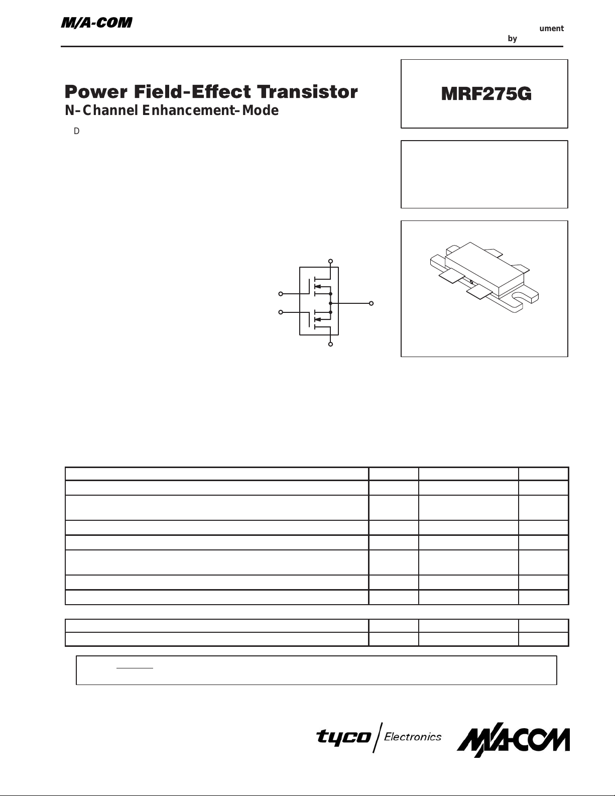
G
G
D
(FLANGE)
D
MRF275G
150 W, 28 V, 500 MHz
N–CHANNEL MOS
BROADBAND
100 – 500 MHz
RF POWER FET
S
CASE 375–04, STYLE 2
MAXIMUM RATINGS
Rating Symbol Value Unit
Drain–Source Voltage V
Drain–Gate Voltage
(RGS = 1.0 MΩ)
Gate–Source Voltage V
Drain Current — Continuous I
Total Device Dissipation @ TC = 25°C
Derate above 25°C
Storage Temperature Range T
Operating Junction Temperature T
V
DSS
DGR
GS
D
P
D
stg
J
65 Vdc
65 Vdc
±40 Adc
26 Adc
400
2.27
–65 to +150 °C
200 °C
THERMAL CHARACTERISTICS
Characteristic Symbol Max Unit
Thermal Resistance, Junction to Case R
NOTE – CAUTION – MOS devices are susceptible to damage from electrostatic charge. Reasonable precautions in handling and
packaging MOS devices should be observed.
REV 1
θJC
0.44 °C/W
1
Watts
W/°C
Page 2
ELECTRICAL CHARACTERISTICS (T
Characteristic
= 25°C unless otherwise noted)
C
OFF CHARACTERISTICS (1)
Drain–Source Breakdown Voltage
(VGS = 0, ID = 50 mA)
Zero Gate Voltage Drain Current
(VDS = 28 V, VGS = 0)
Gate–Source Leakage Current
(VGS = 20 V, VDS = 0)
ON CHARACTERISTICS (1)
Gate Threshold Voltage (VDS = 10 V, ID = 100 mA) V
Drain–Source On–Voltage (VGS = 10 V, ID = 5 A) V
Forward Transconductance (VDS = 10 V, ID = 2.5 A) g
DYNAMIC CHARACTERISTICS (1)
Input Capacitance (VDS = 28 V, VGS = 0, f = 1 MHz) C
Output Capacitance (VDS = 28 V, VGS = 0, f = 1 MHz) C
Reverse Transfer Capacitance (VDS = 28 V, VGS = 0, f = 1 MHz) C
FUNCTIONAL CHARACTERISTICS (2) (Figure 1)
Common Source Power Gain
(VDD = 28 V, P
Drain Efficiency
(VDD = 28 V, P
Electrical Ruggedness
(VDD = 28 V, P
VSWR 30:1 at all Phase Angles)
1. Each side of device measured separately.
2. Measured in push–pull configuration.
= 150 W, f = 500 MHz, IDQ = 2 x 100 mA)
out
= 150 W, f = 500 MHz, IDQ = 2 x 100 mA)
out
= 150 W, f = 500 MHz, IDQ = 2 x 100 mA,
out
Symbol Min Typ Max Unit
V
(BR)DSS
I
DSS
I
GSS
GS(th)
DS(on)
fs
iss
oss
rss
G
ps
η 50 55 — %
ψ
65 — — Vdc
— — 1 mA
— — 1 µA
1.5 2.5 4.5 Vdc
0.5 0.9 1.5 Vdc
3 3.75 — mhos
— 135 — pF
— 140 — pF
— 17 — pF
10 11.2 — dB
No Degradation in Output Power
REV 1
2
Page 3
A
B
+V
GG
C14
B1
B1 Balun, 50 Ω, 0.086″ O.D. 2″ Long, Semi Rigid Coax
B2 Balun, 50 Ω, Coax 0.141″ O.D. 2″ Long, Semi Rigid
C1, C2, C3, C4,
C10, C11, C12, C13 270 pF, ATC Chip Capacitor
C5, C8 1.0–20 pF, Trimmer Capacitor, Johanson
C6 22 pF, Mini–Unelco Capacitor
C7 15 pF, Unelco Capacitor
C9 2.1 pF, ATC Chip Capacitor
C14, C15, C16,
C20, C21, C22 0.1 µF, Ceramic Capacitor
C17, C18 680 pF, Feedthru Capacitor
C19 10 µF, 50 V, Electrolytic Capacitor, Tantalum
L1, L2 10 Turns AWG #24,
L3, L4 10 Turns AWG #18,
R1
C1
Z1
C2
C5 C6 C7 C8
C3
Z2
C4
0.145″ O.D., 106 nH
T aylor–Spring Inductor
0.340″ I.D., Enameled Wire
C15
L1
Z3 Z7Z5
Z4
L2
C20 C21
C16
D.U.T.
Figure 1. 500 MHz T est Circuit
C11
C12
L6
C19
B2
+28 V
+
C17 C18
L5
C22
L3
C10
C9
Z8Z6
C13
L4
BA
L5 Ferroxcube VK200 20/4B
L6 4 Turns #16, 0.340″ I.D.,
Enameled Wire
R1 1.0 kΩ,1/4 W Resistor
W1 – W4 20 x 200 x 250 mils, Wear Pads,
Beryllium–Copper , (See
Component Location Diagram)
Z1, Z2 1.10″ x 0.245″, Microstrip Line
Z3, Z4, Z5, Z6 0.300″ x 0.245″, Microstrip Line
Z7, Z8 1.00″ x 0.245″, Microstrip Line
Board material 0.060″ Teflon–fiberglass,
εr = 2.55, copper clad both sides, 2 oz. copper.
Points A are connected together on PCB.
Points B are connected together on PCB.
REV 1
3
Page 4
TYPICAL CHARACTERISTICS
300
250
200
150
100
, OUTPUT POWER (WATTS)
out
P
50
0
515
10
Pin, INPUT POWER (Watts)
225 MHz
Figure 2. Output Power versus Input Power
10
VDS = 10 V
9
V
= 2.5 V
GS(th)
8
7
6
5
4
3
, DRAIN CURRENT (AMPS)
D
I
2
1
0
0
VGS, GATE–SOURCE VOLTAGE (V)
2
315
400 MHz
IDQ = 2 x 100 mA
VDD = 28 V
20
4
500 MHz
4.52.50.5 3.51.5
160
140
120
100
80
60
–2
VDS = 28 V
IDQ = 2 x 100 mA
Pin = Constant
f = 500 MHz
42
, OUTPUT POWER (WATTS)
40
out
P
20
0
25
–10 00
–8
–6 –4
VGS, GATE–SOURCE VOLTAGE (V)
Figure 3. Output Power versus Gate Voltage
180
Pin = 14 W
10 W
6 W
IDQ = 2 x 100 mA
f = 500 MHz
22 26
24
, OUTPUT POWER (WATTS)
out
P
160
140
120
100
80
60
40
20
0
14 1612
18 20 28
VDD, SUPPLY VOLTAGE (V)
Figure 4. Drain Current versus Gate Voltage
(Transfer Characteristics)
200
180
160
140
120
100
, OUTPUT POWER (WATTS)
out
P
80
60
40
20
0
14 1612 18 20 282422 26
VDD, SUPPLY VOLTAGE (V)
Pin = 14 W
IDQ = 2 x 100 mA
f = 400 MHz
Figure 6. Output Power versus Supply Voltage
REV 1
4
10 W
6 W
Figure 5. Output Power versus Supply Voltage
250
200
150
100
, OUTPUT POWER (WATTS)
out
P
50
0
14 1612 18 20 282422 26
VDD, SUPPLY VOLTAGE (V)
IDQ = 2 x 100 mA
f = 225 MHz
Figure 7. Output Power versus Supply Voltage
12 W
10 W
Pin = 4 W
Page 5
TYPICAL CHARACTERISTICS
1000
C
oss
C, CAPACITANCE (pF)
100
10
1
515
10
VDS, DRAIN–SOURCE VOLTAGE (V)
C
iss
C
rss
VGS = 0 V
f = 1.0 MHz
20
25
Figure 8. Capacitance versus Drain–Source V oltage*
*Data shown applies only to one half of
device, MRF275G
100
10
1.3
VDD = 28 V
1.2
1.1
1
0.9
0.8
, GATE–SOURCE VOLTAGE (NORMALIZED)
GS
V
0.7
30
–25 1750
25
500 100
75 125
TC, CASE TEMPERATURE (°C)
3 A
ID = 4 A
2 A
0.1 A
150
200
Figure 9. Gate–Source V oltage versus
Case T emperature
TC = 25°C
, DRAIN CURRENT (AMPS)
D
I
1
1 100
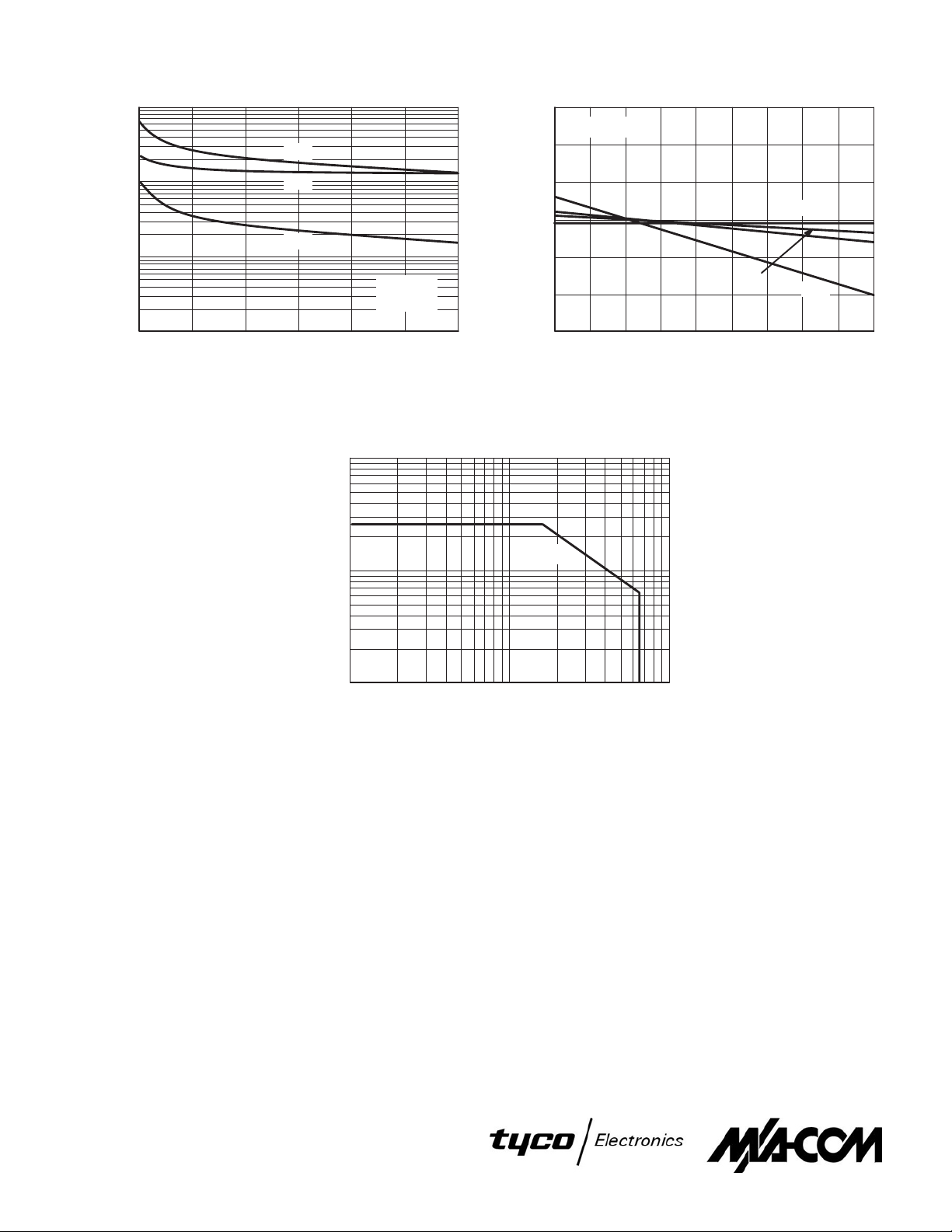
VDS, DRAIN–SOURCE VOLTAGE (V)
10
Figure 10. DC Safe Operating Area
REV 1
5
Page 6

f = 500 MHz
VDD = 28 V, IDQ = 2 x 100 mA, P
f
(MHz)
225 1.6 – j2.30 3.2 – j1.50
400 1.9 + j0.48 2.3 – j0.19
500 1.9 + j2.60 2.0 + j1.30
Z
in
Ohms
= 150 W
out
ZOL*
Ohms
ZOL* = Conjugate of the optimum load impedance
ZOL* = into which the device operates at a given
ZOL* = output power, voltage and frequency.
Note: Input and output impedance values given are
measured from gate to gate and drain to
drain respectively.
Z
400
in
f = 500 MHz
225
400
Zo = 10 Ω
ZOL*
225
Figure 11. Series Equivalent Input/Output Impedance
REV 1
6
Page 7

A
B
BIAS
C10 C11
C1
B1
B1 Balun, 50 Ω, 0.086″ O.D. 2″ Long,
B2 Balun, 50 Ω, 0.141″ O.D. 2″ Long,
C1, C2, C8, C9 270 pF, ATC Chip Capacitor
C3, C5, C7 1.0–20 pF, Trimmer Capacitor
C4 15 pF, ATC Chip Capacitor
C6 33 pF, ATC Chip Capacitor
C10, C12, C13,
C16, C17 0.01 µF, Ceramic Capacitor
C11 1.0 µF, 50 V, Tantalum
C14, C15 680 pF, Feedthru Capacitor
C18 20 µF, 50 V, Tantalum
C3 C4
C2
Semi Rigid Coax
Semi Rigid Coax
R1
L1
L2
C14 C15
C12 C13
Z1 Z3 Z5
C5
Z2
R2
D.U.T.
R3
C16 C17
L1, L2 #18 Wire, Hairpin Inductor
L3, L4 12 Turns #18, 0.340″ I.D.,
L5 Ferroxcube VK200 20/4B
L6 3 Turns #16, 0.340″ I.D.,
R1 1.0 kΩ, 1/4 W Resistor
R2, R3 10 kΩ, 1/4 W Resistor
Z1, Z2 0.400″ x 0.250″, Microstrip Line
Z3, Z4 0.870″ x 0.250″, Microstrip Line
Z5, Z6 0.500″ x 0.250″, Microstrip Line
Board material 0.060″ Teflon–fiberglass,
εr = 2.55, copper clad both sides, 2 oz. copper.
L3
C6
Z4 Z6
L4
BA
L5 L6
C8
C7
C9
0.180″
Enameled Wire
Enameled Wire
C18
28 V
B2
0.200″
REV 1
7
Figure 12. 400 MHz T est Circuit
Page 8

BIAS 0–6 V
R1
C3 C4
C8 C9
L2
C10
+
28 V
–
R2
T1
C5
C1 C2
C1 8.0–60 pF, Arco 404
C2, C3, C7, C8 1000 pF, Chip Capacitor
C4, C9 0.1 µF, Chip Capacitor
C5 180 pF, Chip Capacitor
C6 100 pF and 130 pF,
Chips in Parallel
C10 0.47 µF, Chip Capacitor, 1215 or
Equivalent, Kemet
L1 10 Turns AWG #16, 1/4″ I.D.,
Enamel Wire, Close Wound
L2 Ferrite Beads of Suitable Material
for 1.5–2.0 µH Total Inductance
Board material 062″ fiberglass (G10),
εr ^ 5, Two sided, 1 oz. Copper.
Unless otherwise noted, all chip capacitors
are ATC Type 100 or Equivalent.
D.U.T.
C6
R1 100 Ω, 1/2 W
R2 1.0 k Ω, 1/2 W
T1 4:1 Impedance Ratio, RF Transformer
T2 1:9 Impedance Ratio, RF Transformer.
NOTE: For stability, the input transformer T1 should be loaded
NOTE: with ferrite toroids or beads to increase the common
NOTE: mode inductance. For operation below 100 MHz. The
NOTE: same is required for the output transformer.
T2
Can Be Made of 25 Ω, Semi Rigid Coax,
47–52 Mils O.D.
Can Be Made of 15–18 Ω, Semi Rigid
Coax, 62–90 Mils O.D.
L1
C7
Figure 13. 225 MHz T est Circuit
REV 1
8
Page 9

R1
C14
B1
C15
L1
L3
L5
C17 C18
C16
BEADS 1–3
C22
+
C19
L6
C1
C2
C3
C4
W3 W4
C8
L4
BEADS 4–6
C5
C6 C7
W2 W1
L2
C20
MRF275G JL
Figure 14. MRF275G Component Location (500 MHz)
C10
C11
C9
C12
C13
B2
C21
(Not to Scale)
REV 1
9
MRF275G
JL
Figure 15. MRF275G Circuit Board Photo Master (500 MHz)
(Scale 1:1)
Page 10

NOTE: S–Parameter data represents measurements taken from one chip only.
f
ÁÁÁÁ
ÁÁÁÁ
ÁÁÁÁ
ÁÁÁÁ
ÁÁÁÁ
ÁÁÁÁ
ÁÁÁÁ
ÁÁÁÁ
ÁÁÁÁ
ÁÁÁÁ
ÁÁÁÁ
ÁÁÁÁ
ÁÁÁÁ
ÁÁÁÁ
ÁÁÁÁ
ÁÁÁÁ
ÁÁÁÁ
ÁÁÁÁ
ÁÁÁÁ
ÁÁÁÁ
ÁÁÁÁ
ÁÁÁÁ
ÁÁÁÁ
ÁÁÁÁ
ÁÁÁÁ
ÁÁÁÁ
ÁÁÁÁ
ÁÁÁÁ
ÁÁÁÁ
ÁÁÁÁ
ÁÁÁÁ
ÁÁÁÁ
ÁÁÁÁ
ÁÁÁÁ
ÁÁÁÁ
ÁÁÁÁ
ÁÁÁÁ
ÁÁÁÁ
ÁÁÁÁ
ÁÁÁÁ
T able 1. Common Source S–Parameters (VDS = 12 V, ID = 4.5 A)
MHz
30
40
50
60
70
80
90
100
110
120
130
140
150
160
170
180
190
200
210
220
230
240
250
260
270
280
290
300
310
320
330
340
350
360
370
380
390
400
410
420
S
11
S
21
S
12
S
22
|S11| φ |S21| φ |S12| φ |S22| φ
0.822
0.846
0.842
0.838
0.836
0.841
0.849
0.857
0.864
0.868
0.871
0.874
0.876
0.880
0.885
0.891
0.896
0.900
0.904
0.907
0.909
0.912
0.915
0.918
0.922
0.925
0.927
0.930
0.932
0.934
0.936
0.938
0.941
0.943
0.944
0.945
0.947
0.948
0.949
0.951
–172
–173
–174
–175
–175
–176
–176
–176
–176
–176
–176
–176
–176
–176
–177
–177
–177
–177
–177
–177
–177
–178
–178
–178
–178
–179
–179
–179
–179
–180
–180
180
180
179
179
179
179
179
178
178
6.34
4.32
3.62
3.03
2.76
2.43
2.19
1.89
1.66
1.43
1.25
1.15
1.11
1.06
1.01
0.96
0.87
0.77
0.69
0.63
0.60
0.58
0.58
0.56
0.54
0.49
0.43
0.41
0.40
0.39
0.35
0.38
0.35
0.33
0.30
0.29
0.28
0.26
0.26
0.25
91
81
79
79
80
78
74
68
63
60
59
59
59
59
55
51
45
43
42
43
43
44
42
40
34
32
28
30
32
31
32
31
28
23
21
21
22
25
24
25
0.027
0.027
0.027
0.027
0.028
0.029
0.029
0.028
0.026
0.024
0.023
0.023
0.023
0.023
0.023
0.023
0.022
0.020
0.018
0.017
0.018
0.017
0.017
0.016
0.015
0.014
0.013
0.013
0.013
0.012
0.011
0.011
0.011
0.011
0.011
0.009
0.008
0.008
0.010
0.010
3
–6
–8
–5
–3
–4
–7
–13
–19
–19
–19
–17
–16
–17
–18
–23
–26
–26
–25
–23
–23
–22
–20
–20
–24
–27
–27
–23
–14
–9
–9
–12
–12
–10
–4
1
3
4
5
11
0.946
0.859
0.863
0.923
1.010
1.080
1.150
1.110
1.050
0.958
0.905
0.914
0.969
1.060
1.130
1.190
1.140
1.050
0.958
0.924
0.981
0.981
1.040
1.150
1.170
1.130
1.010
0.964
0.936
0.948
1.000
1.070
1.100
1.120
1.080
1.020
0.966
0.936
1.010
1.040
–173
–172
–175
–177
–178
–178
–176
–176
–177
–175
–176
–177
–178
–178
–177
–178
–179
–177
–176
–175
–178
–180
–179
–180
179
–180
–178
–178
–178
180
180
178
180
–180
180
180
–180
–179
179
178
REV 1
10
Page 11

T able 1. Common Source S–Parameters (VDS = 12 V, ID = 4.5 A) continued
f
ÁÁÁÁ
ÁÁÁÁ
ÁÁÁÁ
ÁÁÁÁ
ÁÁÁÁ
ÁÁÁÁ
ÁÁÁÁ
ÁÁÁÁ
ÁÁÁÁ
ÁÁÁÁ
ÁÁÁÁ
ÁÁÁÁ
ÁÁÁÁ
f
ÁÁÁÁ
ÁÁÁÁ
ÁÁÁÁ
ÁÁÁÁ
ÁÁÁÁ
ÁÁÁÁ
ÁÁÁÁ
ÁÁÁÁ
ÁÁÁÁ
ÁÁÁÁ
ÁÁÁÁ
ÁÁÁÁ
ÁÁÁÁ
ÁÁÁÁ
ÁÁÁÁ
ÁÁÁÁ
ÁÁÁÁ
ÁÁÁÁ
ÁÁÁÁ
ÁÁÁÁ
ÁÁÁÁ
ÁÁÁÁ
ÁÁÁÁ
ÁÁÁÁ
ÁÁÁÁ
MHz
430
440
450
460
470
480
490
500
600
700
800
900
1000
MHz
30
40
50
60
70
80
90
100
110
120
130
140
150
160
170
180
190
200
210
220
230
240
250
260
270
S
11
S
21
S
12
S
22
|S11| φ |S21| φ |S12| φ |S22| φ
0.952
0.953
0.955
0.956
0.956
0.957
0.958
0.960
0.956
0.958
0.962
0.965
0.964
178
177
177
177
177
176
176
176
175
172
170
168
165
0.25
0.24
0.24
0.21
0.20
0.19
0.19
0.19
0.18
0.11
0.10
0.08
0.07
22
19
16
15
16
18
18
19
12
14
12
16
12
0.010
0.009
0.008
0.008
0.009
0.010
0.010
0.010
0.007
0.018
0.029
0.021
0.021
19
22
21
11
16
27
40
46
49
61
51
72
57
1.080
1.100
1.100
1.080
0.992
0.975
0.974
1.010
0.940
0.989
0.967
0.973
1.010
177
178
179
177
178
179
178
177
175
173
172
170
168
T able 2. Common Source S–Parameters (VDS = 24 V, ID = 0.35 mA)
S
11
|S11| φ |S21| φ |S12| φ |S22| φ
0.829
0.858
0.852
0.846
0.843
0.847
0.855
0.865
0.872
0.874
0.876
0.878
0.880
0.883
0.888
0.894
0.899
0.902
0.905
0.907
0.909
0.912
0.915
0.918
0.922
–170
–172
–173
–174
–175
–175
–175
–176
–176
–176
–176
–176
–176
–176
–177
–177
–177
–177
–177
–177
–178
–178
–178
–178
–178
9.20
6.30
5.28
4.42
4.01
3.53
3.18
2.75
2.43
2.10
1.84
1.70
1.63
1.56
1.49
1.42
1.29
1.14
1.02
0.94
0.89
0.87
0.86
0.83
0.80
S
21
92
83
80
80
81
80
76
70
65
62
61
61
61
61
58
53
47
45
44
46
45
46
44
42
36
0.023
0.022
0.023
0.023
0.024
0.024
0.024
0.023
0.022
0.020
0.019
0.019
0.019
0.019
0.019
0.019
0.018
0.017
0.015
0.015
0.015
0.014
0.014
0.014
0.013
S
12
4
–4
–6
–3
–1
–2
–5
–10
–16
–16
–15
–14
–13
–13
–14
–18
–22
–24
–23
–19
–16
–15
–15
–17
–19
0.915
0.834
0.836
0.892
0.978
1.050
1.110
1.080
1.020
0.932
0.882
0.889
0.943
1.030
1.100
1.160
1.120
1.030
0.941
0.903
0.957
0.961
1.020
1.120
1.140
S
22
–171
–170
–174
–175
–177
–177
–176
–175
–176
–174
–175
–176
–177
–177
–176
–176
–177
–176
–175
–174
–177
–179
–178
–178
–180
REV 1
11
Page 12

f
MHz
ÁÁÁÁ
ÁÁÁÁ
ÁÁÁÁ
ÁÁÁÁ
ÁÁÁÁ
ÁÁÁÁ
ÁÁÁÁ
ÁÁÁÁ
ÁÁÁÁ
ÁÁÁÁ
ÁÁÁÁ
ÁÁÁÁ
ÁÁÁÁ
ÁÁÁÁ
ÁÁÁÁ
ÁÁÁÁ
ÁÁÁÁ
ÁÁÁÁ
ÁÁÁÁ
ÁÁÁÁ
ÁÁÁÁ
ÁÁÁÁ
ÁÁÁÁ
ÁÁÁÁ
ÁÁÁÁ
ÁÁÁÁ
ÁÁÁÁ
ÁÁÁÁ
f
ÁÁÁÁ
ÁÁÁÁ
ÁÁÁÁ
ÁÁÁÁ
ÁÁÁÁ
ÁÁÁÁ
ÁÁÁÁ
ÁÁÁÁ
ÁÁÁÁ
ÁÁÁÁ
ÁÁÁÁ
280
290
300
310
320
330
340
350
360
370
380
390
400
410
420
430
440
450
460
470
480
490
500
600
700
800
900
1000
T able 2. Common Source S–Parameters (VDS = 24 V, ID = 0.35 mA) continued
S
11
|S11| φ |S21| φ |S12| φ |S22| φ
0.925
0.927
0.929
0.931
0.932
0.934
0.937
0.939
0.941
0.943
0.944
0.945
0.946
0.947
0.949
0.950
0.952
0.953
0.954
0.955
0.956
0.957
0.958
0.956
0.959
0.963
0.968
0.969
–179
–179
–179
–179
–180
–180
180
180
179
179
179
179
178
178
178
178
177
177
177
177
176
176
176
175
172
170
168
165
0.73
0.65
0.62
0.60
0.57
0.53
0.56
0.53
0.50
0.46
0.44
0.41
0.40
0.38
0.38
0.37
0.36
0.36
0.31
0.30
0.29
0.29
0.28
0.24
0.16
0.14
0.12
0.09
S
21
34
32
32
34
33
34
33
30
25
23
22
24
27
26
26
23
21
18
17
17
19
20
20
12
13
10
11
7
0.013
0.011
0.011
0.010
0.010
0.010
0.010
0.010
0.010
0.009
0.009
0.008
0.008
0.009
0.009
0.009
0.009
0.009
0.009
0.009
0.009
0.010
0.010
0.006
0.019
0.023
0.026
0.025
S
12
–20
–18
–15
–9
–6
–4
–2
0
0
0
2
8
16
20
22
25
26
28
24
29
36
45
50
90
63
63
84
70
1.110
0.994
0.948
0.916
0.934
0.985
1.050
1.090
1.110
1.080
1.010
0.956
0.926
1.000
1.040
1.070
1.090
1.090
1.070
0.990
0.963
0.959
0.996
0.924
0.986
0.963
0.967
1.000
S
22
–179
–177
–177
–177
–180
–180
179
–179
–178
–179
–179
–179
–178
–180
179
179
180
–180
178
179
–179
180
178
176
174
173
171
169
MHz
30
40
50
60
70
80
90
100
110
120
130
REV 1
12
T able 3. Common Source S–Parameters (VDS = 28 V, ID = 0.39 mA)
S
11
|S11| φ |S21| φ |S12| φ |S22| φ
0.834
0.863
0.857
0.851
0.848
0.852
0.860
0.869
0.876
0.878
0.879
–169
–172
–173
–174
–175
–175
–175
–176
–176
–176
–176
10.08
6.91
5.79
4.86
4.41
3.87
3.49
3.03
2.68
2.31
2.03
S
21
93
83
81
81
82
80
77
71
66
63
62
0.021
0.021
0.021
0.022
0.022
0.022
0.023
0.022
0.021
0.019
0.018
S
12
4
–4
–5
–3
–1
–1
–5
–9
–14
–14
–15
0.807
0.828
0.830
0.883
0.970
1.040
1.100
1.070
1.010
0.923
0.876
S
22
–171
–170
–173
–175
–177
–177
–176
–175
–176
–174
–175
Page 13

T able 3. Common Source S–Parameters (VDS = 28 V, ID = 0.39 mA) continued
f
ÁÁÁÁ
ÁÁÁÁ
ÁÁÁÁ
ÁÁÁÁ
ÁÁÁÁ
ÁÁÁÁ
ÁÁÁÁ
ÁÁÁÁ
ÁÁÁÁ
ÁÁÁÁ
ÁÁÁÁ
ÁÁÁÁ
ÁÁÁÁ
ÁÁÁÁ
ÁÁÁÁ
ÁÁÁÁ
ÁÁÁÁ
ÁÁÁÁ
ÁÁÁÁ
ÁÁÁÁ
ÁÁÁÁ
ÁÁÁÁ
ÁÁÁÁ
ÁÁÁÁ
ÁÁÁÁ
ÁÁÁÁ
ÁÁÁÁ
ÁÁÁÁ
ÁÁÁÁ
ÁÁÁÁ
ÁÁÁÁ
ÁÁÁÁ
ÁÁÁÁ
ÁÁÁÁ
ÁÁÁÁ
ÁÁÁÁ
ÁÁÁÁ
ÁÁÁÁ
ÁÁÁÁ
ÁÁÁÁ
ÁÁÁÁ
ÁÁÁÁ
MHz
140
150
160
170
180
190
200
210
220
230
240
250
260
270
280
290
300
310
320
330
340
350
360
370
380
390
400
410
420
430
440
450
460
470
480
490
500
600
700
800
900
1000
S
11
S
21
S
12
S
22
|S11| φ |S21| φ |S12| φ |S22| φ
0.881
0.883
0.886
0.890
0.896
0.901
0.904
0.907
0.908
0.910
0.912
0.916
0.919
0.922
0.925
0.927
0.929
0.931
0.933
0.934
0.937
0.939
0.941
0.943
0.944
0.945
0.946
0.947
0.949
0.950
0.951
0.953
0.953
0.954
0.955
0.956
0.957
0.955
0.958
0.963
0.966
0.968
–176
–176
–177
–177
–177
–177
–177
–177
–177
–178
–178
–178
–178
–179
–179
–179
–179
–179
–180
–180
180
180
179
179
179
179
178
178
178
178
177
177
177
177
176
176
176
174
172
170
168
165
1.87
1.79
1.72
1.64
1.56
1.42
1.26
1.13
1.03
0.99
0.96
0.95
0.93
0.89
0.81
0.72
0.69
0.66
0.63
0.59
0.62
0.59
0.55
0.51
0.49
0.46
0.44
0.43
0.42
0.41
0.40
0.39
0.35
0.33
0.32
0.32
0.31
0.26
0.18
0.15
0.13
0.10
62
62
62
58
54
48
46
45
47
46
47
45
42
37
35
33
33
35
34
35
34
31
26
24
23
25
27
26
27
24
21
19
17
18
19
20
21
13
12
0.018
0.018
0.018
0.018
0.018
0.018
0.017
0.015
0.013
0.014
0.014
0.014
0.013
0.012
0.012
0.011
0.011
0.012
0.011
0.009
0.009
0.010
0.010
0.009
0.008
0.008
0.007
0.010
0.012
0.010
0.008
0.008
0.009
0.010
0.012
0.012
0.010
0.012
0.018
9
9
6
0.020
0.028
0.033
–13
–11
–11
–12
–16
–21
–19
–14
–13
–15
–13
–10
–12
–15
–16
–16
–10
5
16
14
3
4
8
11
17
24
20
19
29
41
40
34
26
30
43
60
65
67
64
89
81
73
0.884
0.934
1.020
1.090
1.150
1.110
1.030
0.938
0.897
0.948
0.956
1.020
1.120
1.140
1.110
0.988
0.944
0.920
0.936
0.989
1.050
1.080
1.110
1.070
1.010
0.949
0.922
0.995
1.030
1.060
1.090
1.090
1.070
0.983
0.964
0.956
0.993
0.926
0.984
0.961
0.967
0.997
–176
–177
–177
–176
–176
–177
–176
–175
–174
–176
–179
–178
–178
–179
–178
–176
–177
–177
–180
–180
180
–179
–178
–179
–178
–178
–178
–180
179
179
180
–180
178
179
–180
179
178
176
174
173
171
169
REV 1
13
Page 14

Figure 16. MRF275G T est Fixture
RF POWER MOSFET CONSIDERA TIONS
MOSFET CAPACITANCES
The physical structure of a MOSFET results in capacitors
between the terminals. The metal oxide gate structure determines the capacitors from gate–to–drain (Cgd), and gate–to–
source (Cgs). The PN junction formed during the fabrication
of the MOSFET results in a junction capacitance from drain–
to–source (Cds).
These capacitances are characterized as input (C
put (C
) and reverse transfer (C
oss
) capacitances on data
rss
iss
), out-
sheets. The relationships between the inter–terminal capacitances and those given on data sheets are shown below. The
C
can be specified in two ways:
iss
1. Drain shorted to source and positive voltage at the gate.
2. Positive voltage of the drain in respect to source and zero
volts at the gate. In the latter case the numbers are lower.
However, neither method represents the actual operating conditions in RF applications.
DRAIN
C
ds
SOURCE
C
iss
C
oss
C
rss
= Cgd + C
= Cgd + C
= C
gd
gs
ds
The C
C
gd
GA TE
C
gs
given in the electrical characteristics table was
iss
measured using method 2 above. It should be noted that
C
, C
, C
iss
oss
are measured at zero drain current and are
rss
provided for general information about the device. They are
not RF design parameters and no attempt should be made to
use them as such.
DRAIN CHARACTERISTICS
One figure of merit for a FET is its static resistance in the
full–on condition. This on–resistance, V
DS(on)
, occurs in the
linear region of the output characteristic and is specified under specific test conditions for gate–source voltage and drain
current. For MOSFETs, V
has a positive temperature
DS(on)
coefficient and constitutes an important design consideration
at high temperatures, because it contributes to the power
dissipation within the device.
GATE CHARACTERISTICS
The gate of the MOSFET is a polysilicon material, and is
electrically isolated from the source by a layer of oxide. The
input resistance is very high — on the order of 109 ohms —
resulting in a leakage current of a few nanoamperes.
Gate control is achieved by applying a positive voltage
slightly in excess of the gate–to–source threshold voltage,
V
GS(th)
.
Gate Voltage Rating — Never exceed the gate voltage
rating (or any of the maximum ratings on the front page). Exceeding the rated VGS can result in permanent damage to
the oxide layer in the gate region.
Gate Termination — The gates of this device are essentially capacitors. Circuits that leave the gate open–circuited
or floating should be avoided. These conditions can result in
turn–on of the devices due to voltage build–up on the input
capacitor due to leakage currents or pickup.
Gate Protection — These devices do not have an internal
monolithic zener diode from gate–to–source. If gate protection is required, an external zener diode is recommended.
Using a resistor to keep the gate–to–source impedance
low also helps damp transients and serves another important
function. Voltage transients on the drain can be coupled to
the gate through the parasitic gate–drain capacitance. If the
gate–to–source impedance and the rate of voltage change
on the drain are both high, then the signal coupled to the gate
REV 1
14
Page 15

may be large enough to exceed the gate–threshold voltage
and turn the device on.
HANDLING CONSIDERATIONS
When shipping, the devices should be transported only in
antistatic bags or conductive foam. Upon removal from the
packaging, careful handling procedures should be adhered
to. Those handling the devices should wear grounding straps
and devices not in the antistatic packaging should be kept in
metal tote bins. MOSFETs should be handled by the case
and not by the leads, and when testing the device, all leads
should make good electrical contact before voltage is applied. As a final note, when placing the FET into the system it
is designed for, soldering should be done with grounded
equipment.
DESIGN CONSIDERATIONS
The MRF275G is a RF power N–channel enhancement
mode field–effect transistor (FETs) designed for HF, VHF and
UHF power amplifier applications. M/A-COM RF MOSFETs
feature a vertical structure with a planar design.
M/A-COM Application Note AN211A, FETs in Theory and
Practice, is suggested reading for those not familiar with the
construction and characteristics of FETs.
The major advantages of RF power FETs include high
gain, low noise, simple bias systems, relative immunity from
thermal runaway, and the ability to withstand severely mismatched loads without suffering damage. Power output can
be varied over a wide range with a low power dc control signal.
DC BIAS
The MRF275G is an enhancement mode FET and, therefore, does not conduct when drain voltage is applied. Drain
current flows when a positive voltage is applied to the gate.
RF power FETs require forward bias for optimum performance. The value of quiescent drain current (IDQ) is not critical for many applications. The MRF275G was characterized
at IDQ = 100 mA, each side, which is the suggested minimum
value of IDQ. For special applications such as linear amplification, IDQ may have to be selected to optimize the critical
parameters.
The gate is a dc open circuit and draws no current. Therefore, the gate bias circuit may be just a simple resistive divider network. Some applications may require a more elaborate
bias system.
GAIN CONTROL
Power output of the MRF275G may be controlled from its
rated value down to zero (negative gain) by varying the dc
gate voltage. This feature facilitates the design of manual
gain control, AGC/ALC and modulation systems.
REV 1
15
Page 16

P ACKAGE DIMENSIONS
U
G
12
R
5
K
34
Q
RADIUS 2 PL
0.25 (0.010) B
–B–
M
M
A
T
M
D
E
N
H
–A–
J
SEATING
–T–
PLANE
C
NOTES:
1. DIMENSIONING AND TOLERANCING PER ANSI
Y14.5M, 1982.
2. CONTROLLING DIMENSION: INCH.
DIM MIN MAX MIN MAX
A 1.330 1.350 33.79 34.29
B 0.370 0.410 9.40 10.41
C 0.190 0.230 4.83 5.84
D 0.215 0.235 5.47 5.96
E 0.050 0.070 1.27 1.77
G 0.430 0.440 10.92 11.18
H 0.102 0.112 2.59 2.84
J 0.004 0.006 0.11 0.15
K 0.185 0.215 4.83 5.33
N 0.845 0.875 21.46 22.23
Q 0.060 0.070 1.52 1.78
R 0.390 0.410 9.91 10.41
U 1.100 BSC 27.94 BSC
STYLE 2:
PIN 1. DRAIN
2. DRAIN
3. GATE
4. GATE
5. SOURCE
MILLIMETERSINCHES
CASE 375–04
ISSUE D
Specifications subject to change without notice.
n
North America: Tel. (800) 366-2266, Fax (800) 618-8883
n Asia/Pacific: Tel.+81-44-844-8296, Fax +81-44-844-8298
n
Europe: Tel. +44 (1344) 869 595, Fax+44 (1344) 300 020
Visit www.macom.com for additional data sheets and product information.
REV 1
16
 Loading...