

Page 1
SEMICONDUCTOR TECHNICAL DATA
The RF Sub–Micron Bipolar Line
Designed for broadband commercial and industrial applications at frequencies from 1800 to 2000 MHz. The high gain and broadband performance of this
device makes it ideal for large–signal, common–emitter class A and class AB
amplifier applications. Suitable for frequency modulated, amplitude modulated
and multi–carrier base station RF power amplifiers.
• Specified 26 Volts, 2.0 GHz, Class AB, Two–Tones Characteristics
Output Power — 30 Watts (PEP)
Power Gain — 9.8 dB
Efficiency — 34%
Intermodulation Distortion — –28 dBc
• Typical 26 Volts, 1.88 GHz, Class AB, CW Characteristics
Output Power — 30 Watts
Power Gain — 10.5 dB
Efficiency — 40%
• Excellent Thermal Stability
• Capable of Handling 3:1 VSWR @ 26 Vdc, 2000 MHz, 30 Watts (PEP)
Output Power
• Characterized with Series Equivalent Large–Signal Impedance Parameters
• S–Parameter Characterization at High Bias Levels
• Designed for FM, TDMA, CDMA, and Multi–Carrier Applications
Order this document
by MRF20030/D
30 W, 2.0 GHz
NPN SILICON
BROADBAND
RF POWER TRANSISTOR
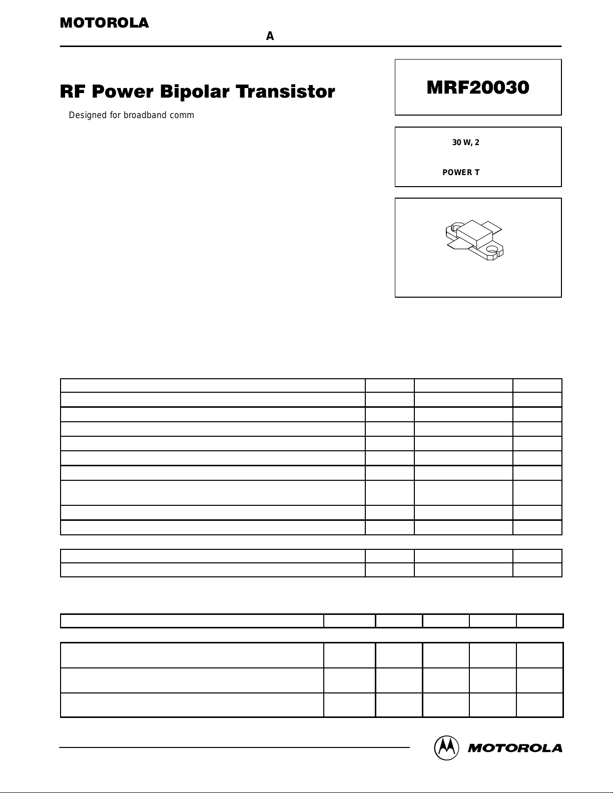
CASE 395D–03, STYLE 1
MAXIMUM RATINGS
Rating Symbol Value Unit
Collector–Emitter Voltage V
Collector–Emitter Voltage V
Collector–Base Voltage V
Collector–Emitter Voltage (RBE = 100 Ω) V
Emitter–Base Voltage V
Collector Current – Continuous I
Total Device Dissipation @ TC = 25°C
Derate above 25°C
Storage Temperature Range T
Operating Junction Temperature T
THERMAL CHARACTERISTICS
Rating Symbol Max Unit
Thermal Resistance, Junction to Case
(1) Thermal resistance is determined under specified RF operating condition.
ELECTRICAL CHARACTERISTICS (T
Characteristic
(1)
= 25°C unless otherwise noted)
C
Symbol Min Typ Max Unit
OFF CHARACTERISTICS
Collector–Emitter Breakdown V oltage
(IC = 25 mAdc, IB = 0)
Collector–Emitter Breakdown Voltage
(IC = 25 mAdc, VBE = 0)
Collector–Base Breakdown Voltage
(IC = 25 mAdc, IE = 0)
V
(BR)CEO
V
(BR)CES
V
(BR)CBO
CEO
CES
CBO
CER
EB
C
P
D
stg
J
R
θJC
25 26 — Vdc
60 70 — Vdc
60 70 — Vdc
25 Vdc
60 Vdc
60 Vdc
30 Vdc
–3 Vdc
4 Adc
125
0.71
– 65 to +150 °C
200 °C
1.4 °C/W
Watts
W/°C
REV 1
Motorola, Inc. 1997
MRF20030MOTOROLA RF DEVICE DATA
1
Page 2

ELECTRICAL CHARACTERISTICS — continued (T
Characteristic
= 25°C unless otherwise noted)
C
OFF CHARACTERISTICS
Emitter–Base Breakdown Voltage
(IB = 5 mAdc, IC = 0)
Collector Cutoff Current
(VCE = 30 Vdc, VBE = 0)
ON CHARACTERISTICS
DC Current Gain
(VCE = 5 Vdc, ICE = 1 Adc)
DYNAMIC CHARACTERISTICS
Output Capacitance
(VCB = 26 Vdc, IE = 0, f = 1.0 MHz)
(1)
FUNCTIONAL TESTS (In Motorola T est Fixture)
Common–Emitter Amplifier Power Gain
(VCC = 26 Vdc, P
f1 = 2000.0 MHz, f2 = 2000.1 MHz)
Collector Efficiency
(VCC = 26 Vdc, P
f1 = 2000.0 MHz, f2 = 2000.1 MHz)
Intermodulation Distortion
(VCC = 26 Vdc, P
f1 = 2000.0 MHz, f2 = 2000.1 MHz)
Input Return Loss
(VCC = 26 Vdc, P
f1 = 2000.0 MHz, f2 = 2000.1 MHz)
Load Mismatch
(VCC = 26 Vdc, P
f1 = 2000.0 MHz, f2 = 2000.1 MHz, Load VSWR = 3:1, All Phase
Angles at Frequency of Test)
Common–Emitter Amplifier Power Gain
(VCC = 26 Vdc, P
f1 = 1930.0 MHz, f2 = 1930.1 MHz)
Collector Efficiency
(VCC = 26 Vdc, P
f1 = 1930.0 MHz, f2 = 1930.1 MHz)
Intermodulation Distortion
(VCC = 26 Vdc, P
f1 = 1930.0 MHz, f2 = 1930.1 MHz)
Input Return Loss
(VCC = 26 Vdc, P
f1 = 1930.0 MHz, f2 = 1930.1 MHz)
= 30 Watts, ICQ = 120 mA,
out
= 30 Watts (PEP), ICQ = 120 mA,
out
= 30 Watts (PEP), ICQ = 120 mA,
out
= 30 Watts (PEP), ICQ = 125 mA,
out
= 30 Watts (PEP), ICQ = 120 mA,
out
= 30 Watts (PEP), ICQ = 125 mA,
out
= 30 Watts (PEP), ICQ = 125 mA,
out
= 30 Watts (PEP), ICQ = 125 mA,
out
= 30 Watts (PEP), ICQ = 125 mA,
out
GUARANTEED BUT NOT TESTED (In Motorola T est Fixture)
Common–Emitter Amplifier Power Gain
(VCC = 26 Vdc, P
Collector Efficiency
(VCC = 26 Vdc, P
Input Return Loss
(VCC = 26 Vdc, P
Output Mismatch Stress
(VCC = 25 Vdc, P
f = 1880 MHz, VSWR = 3:1, All Phase Angles at Frequency of Test)
(1) For Information Only. This Part Is Collector Matched.
= 30 Watts, ICQ = 125 mA, f = 1880 MHz)
out
= 30 Watts , ICQ = 125 mA, f = 1880 MHz)
out
= 30 Watts , ICQ = 125 mA, f = 1880 MHz)
out
= 30 Watts, ICQ = 125 mA,
out
Symbol Min Typ Max Unit
V
(BR)EBO
I
CES
h
FE
C
ob
G
pe
η 34 38 — %
IMD — –33 –28 dBc
IRL 10 17 — dB
ψ
G
pe
η — 34 — %
IMD — –35 — dBc
IRL — 14 — dB
G
pe
η — 40 — %
IRL — 14 — dB
ψ
3 3.8 — Vdc
— — 10 mAdc
20 40 80 —
— 28 — pF
9.8 10.5 — dB
No Degradation in Output Power
— 10.5 — dB
— 10.5 — dB
Typically No Degradation in Output Power
MRF20030
2
MOTOROLA RF DEVICE DATA
Page 3

V
BB
R1
B1, B2 Ferrite Bead, P/N 5659065/3B, Ferroxcube
C1, C13 0.1 µF, Chip Capacitor, Kermet
C2 100 µF, 50 V, Electrolytic Capacitor, Mallory
C3, C5, C12 0.6–4 pF, Variable Capacitor, Johanson, Gigatrim
C4, C11 10 pF, B Case Chip Capacitor, ATC
C6, C8 24 pF, B Case Chip Capacitor, ATC
C7, C9 75 pF, B Case Chip Capacitor, ATC
C10 0.4–2.5 pF, Variable Capacitor, Johanson, Gigatrim
C14 470 µF, 63 V, Electrolytic Capacitor, Mallory
D1 Diode, Motorola (MUR3160T3)
L1, L4 12 Turns, 22 AWG, IDIA. 0.195″
L2, L3 0.750″ 20 AWG
D1
Q1
R2
Q2
R3
INPUT
RF
L1
+
C1 C2
R4
Z1 Z2 Z3 Z4
C3 C5
R5
C4
B1
R6
L2
C6
C7
L4
B2
C8
R8
C9
R7
L4
Z5 Z6 Z7
DUT
N1, N2 Type N Flange Mount RF Connector
R1, R2 130 Ω, 1/8 W Chip Resistor, Rohm
R3, R4 100 Ω, 1/8 W Chip Resistor, Rohm
R5, R8 10 Ω, 1/2 W Resistor
R6, R7 10 Ω, 1/8 W Chip Resistor, Rohm (10J)
Q1 Transistor, PNP Motorola (BD136)
Q2 Transistor, NPN Motorola (MJD47)
Board 30 Mil Glass Teflon, Arlon GX–0300–55–22,
C10
MA/COM 3052–1648–10
εr = 2.55
C11
C13 C14
Z8
C12
V
CC
+
RF
OUT
Figure 1. Class AB T est Fixture Electrical Schematic
MRF20030MOTOROLA RF DEVICE DATA
3
Page 4

V
supply
R1
+
C2
RF
NPUT
R2
R5
Q1
R3
R4
N1
Z1 Z2 Z3 Z5
C1
Q2
C3
C4
Z4
R7
L1
V
CC
R6
R8
C6
B1
C5 C7
DUT
+
C8
C11 C12
L2
C10
Z6
Z7
C9
Z8 Z9
B2
R9
Z10
C13
V
CC
+
C14 C15
N2
RF
OUTPUT
B1, B2 Long Bead, Fair Rite
C1, C9, C13 0.6–4 pF, Variable Capacitor, Johanson, Gigatrim
C2, C8 100 µF, 50 V, Electrolytic Capacitor, Mallory
C3, C10 18 pF B Case Chip Capacitor, ATC
C4 1.3 pF, B Case Chip Capacitor, ATC
C5, C11 24 pF, B Case Chip Capacitor, ATC
C6, C14 0.1 mF, Chip Capacitor, Kermet
C7, C12 75 pF, B Case Chip Capacitor, ATC
C15 470 mF, 63 V, Electrolytic Capacitor, Mallory
L1, L2 0.75 in., 20 AWG
N1, N2 Type N Flange Mount RF
Connector, MA/COM
Figure 2. Class A T est Fixture Electrical Schematic
Q1 Transistor, NPN, Motorola (BD135)
Q2 Transistor, PNP, Motorola (BD136)
R1 250 W, Chip Resistor, 1/8 Watt, Rohm
R2 500 W, 1/4 Watt, Potentiometer
R3 4.7 kW, Chip Resistor, 1/8 Watt, Rohm
R4 2 x 4.7 kW, Chip Resistor, 1/8 Watt, Rohm
R5 1.0 W, 10 Watt, Resistor, DALE
R6 39 W, 1 Watt, Resistor
R7, R9 4 x 39 W, Chip Resistors, 1/8 Watt, Rohm
R8 75 W, Chip Resistor, 1/8 Watt, Rohm
Board 30 Mil Glass Teflon, Arlon GX–0300–55–22,
εr = 2.55
MRF20030
4
MOTOROLA RF DEVICE DATA
Page 5

TYPICAL CHARACTERISTICS
35
30
25
20
15
10
, OUTPUT POWER (WATTS)
out
P
–20
–30
–40
–50
–60
IMD, INTERMODULATION DISTORTION (dBc)
–70
G
pe
VCC = 26 Vdc
5
0
135
Pin, INPUT POWER (WATTS)
ICQ = 125 mA
f = 2000 MHz Single Tone
2
Figure 3. Output Power & Power Gain
versus Input Power
3rd Order
5th Order
7th Order
VCC = 26 Vdc
ICQ = 125 mA
f1 = 2000.0 MHz
f2 = 2000.1 MHz
0
10 30 40
15525
20
P
, OUTPUT POWER (WATTS) PEP
out
Figure 5. Intermodulation Distortion
versus Output Power
11.5
11
P
out
4
10.5
10
9.5
9
8.5
8
40
35
30
25
20
, GAIN (dB)
pe
15
G
, OUTPUT POWER (WATTS)
10
out
P
5
0
1800 20000
Pin = 3.5 W
2.5 W
1.5 W
1850
1900 1950
f, FREQUENCY (MHz)
VCC = 26 Vdc
ICQ = 125 mA
Figure 4. Output Power versus Frequency
–5
–10
–15
–20
–25
–30
–35
–40
–45
IMD, INTERMODULATION DISTORTION (dBc)
35
11.5
11
10.5
10
9.5
, GAIN (dB)
pe
9
G
8.5
8
7.5
G
pe
P
= 30 W (PEP)
out
ICQ = 125 mA
f1 = 2000.0 MHz
f2 = 2000.1 MHz
20 2218
VCC, COLLECTOR SUPPL Y VOLTAGE (Vdc)
IMD
24 26 28
Figure 6. Power Gain and Intermodulation
Distortion versus Supply V oltage
–25
–30 11
–35
ICQ = 75 mA
–40
–45
125 mA
–50
–55
IMD, INTERMODULATION DISTORTION (dBc)
–60
0.01
250 mA
400 mA
0.1
P
, OUTPUT POWER (WATTS) PEP
out
VCC = 26 Vdc
f1 = 2000.0 MHz
f2 = 2000.1 MHz
1.0 100
10
Figure 7. Intermodulation Distortion
versus Output Power
12
ICQ = 400 mA
250 mA
10
9
125 mA
8
, POWER GAIN (dB)
pe
G
7
6
75 mA
5
0.1
P
, OUTPUT POWER (WATTS) PEP
out
1.0
Figure 8. Power Gain versus Output Power
VCC = 26 Vdc
f1 = 2000.0 MHz
f2 = 2000.1 MHz
10
MRF20030MOTOROLA RF DEVICE DATA
1000.01
5
Page 6

3.5
4
3
MTBF LIMITED
T
flange
= 75°C
11
P
= 30 W (PEP)
out
VCC = 26 Vdc
ICQ = 125 mA
10.5 36
G
pe
38
2.5
2
1.5
1
, COLLECTOR CURRENT (Adc)
C
I
0.5
0
TJ = 175°C
VCE, COLLECTOR SUPPL Y VOLTAGE (Vdc)
T
flange
= 100°C
Figure 9. DC Class A Safe Operating Area
60
40
20
0
, OUTPUT POWER (dBm)
out
P
–20
–40
FUNDAMENT AL
3rd Order
Pin, INPUT POWER (dBm)
VCC = 24 Vdc
ICQ = 1.8 Adc
f1 = 2000.0 MHz
f2 = 2000.1 MHz
Figure 11. Class A Third Order Intercept Point
10
, GAIN (dB)
pe
G
9.5
BREAKDOWN LIMITED
9
2824201612840
Figure 10. Performance in Broadband Circuit
1.E+10
1.E+09
2
1.E+08
1.E+07
1.E+06
1.E+05
1.E+04
MTBF FACTOR (HOURS x AMPS )
1.E+03
50403020100
1.E+02
This above graph displays calculated MTBF in hours x ampere
emitter current. Life tests at elevated temperatures have correlated
to better than
Divide MTBF factor by I
η
VSWR
1950
f, FREQUENCY (MHz)
TJ, JUNCTION TEMPERATURE (°C)
±
10% of the theoretical prediction for metal failure.
2
for MTBF in a particular application.
C
Figure 12. MTBF Factor versus
Junction T emperature
1.7:1
34
COLLECTOR EFFICIENCY (%)INPUT VSWR
32
28
2000190018501800
1.1:1
250200150100500
2
MRF20030
6
MOTOROLA RF DEVICE DATA
Page 7

+j1
0.0
+j0.5
+j0.2
1.95 GHz
2 GHz
1.95 GHz
Z
*
OL
–j0.2
0.2
1.9 GHz
–j0.5
1.85 GHz
Z
in
1.85 GHz
0.5
f = 1.8 GHz
1.9 GHz
f = 1.8 GHz
12
Zo = 10
+j2
+j3
Ω
+j5
+j10
35
–j10
–j5
–j3
–j2
–j1
VCC = 26 V, ICQ = 125 mA, P
f
MHz
1800
1850
1900
1950
Zin(1)
Ω
4.5 + j7.0
4.5 + j6.0
4.5 + j4.6
3.7 + j2.4
= 30 W (PEP)
out
ZOL*
4.7 + j2.4
4.4 + j1.6
3.4 + j1.2
3.3 + j1.6
Ω
2000 3.5 + j1.5 3.5 + j2.0
Zin(1)= Conjugate of fixture base impedance.
ZOL* = Conjugate of the optimum load impedance at
given output power, voltage, bias current and
frequency.
Figure 13. Series Equivalent Input and Output Impedence
MRF20030MOTOROLA RF DEVICE DATA
7
Page 8

T able 1. Common Emitter S–Parameters at VCE = 24 Vdc, IC = 1.8 Adc
f
GHz
1.5 .964 158 .65 74 .046 60 .859 161
1.55 .960 156 .74 68 .047 56 .841 161
1.6 .952 155 .87 60 .049 53 .815 160
1.65 .933 153 1.05 50 .048 46 .787 161
1.7 .892 149 1.32 35 .047 40 .744 163
1.75 .804 149 1.64 13 .040 29 .719 168
1.8 .727 157 1.78 –18 .026 21 .778 175
1.85 .787 163 1.50 –50 .015 54 .883 174
1.9 .873 163 1.14 –73 .020 81 .937 171
1.95 .921 160 .84 –89 .026 88 .949 168
2 .941 157 .62 –102 .031 93 .950 165
2.05 .943 155 .48 –109 .036 93 .946 164
2.1 .940 153 .38 –118 .040 92 .942 163
2.15 .928 151 .30 –127 .042 97 .939 162
2.2 .917 150 .24 –133 .049 99 .935 161
2.25 .907 150 .20 –140 .056 101 .933 160
2.3 .888 148 .17 –150 .066 100 .926 159
2.35 .861 148 .14 –159 .077 98 .916 157
2.4 .853 149 .11 –167 .087 92 .909 157
2.45 .860 146 .10 –176 .095 89 .900 155
2.5 .880 146 .10 156 .119 84 .880 155
|S11|
S
11
∠
f
|S21|
S
21
∠
f
|S12|
S
12
∠
f
|S22|
S
22
∠
f
MRF20030
8
MOTOROLA RF DEVICE DATA
Page 9

P ACKAGE DIMENSIONS
–A–
U
1
W
–B–
3
K
2 PL
2
Q2 PL
D
N
J
H
0.51 (0.020) B
E
C
M
–T–
T
SEATING
PLANE
M
A
M
NOTES:
1. DIMENSIONING AND TOLERANCING PER ANSI
Y14.5M, 1982.
2. CONTROLLING DIMENSION: INCH.
DIM MIN MAX MIN MAX
A 0.739 0.750 18.77 19.05
B 0.240 0.260 6.10 6.60
C 0.165 0.198 4.19 5.03
D 0.215 0.225 5.46 5.72
E 0.060 0.070 1.52 1.78
H 0.084 0.096 2.13 2.44
J 0.004 0.006 0.10 0.15
K 0.178 0.208 4.52 5.28
N 0.315 0.330 8.00 8.38
Q 0.125 0.135 3.18 3.42
U 0.560 BSC 14.23 BSC
W 0.035 0.045 0.89 1.14
STYLE 1:
PIN 1. BASE
2. COLLECTOR
3. EMITTER
MILLIMETERSINCHES
CASE 395D–03
ISSUE B
MRF20030MOTOROLA RF DEVICE DATA
9
Page 10

Motorola reserves the right to make changes without further notice to any products herein. Motorola makes no warranty , representation or guarantee regarding
the suitability of its products for any particular purpose, nor does Motorola assume any liability arising out of the application or use of any product or circuit, and
specifically disclaims any and all liability, including without limitation consequential or incidental damages. “T ypical” parameters which may be provided in Motorola
data sheets and/or specifications can and do vary in different applications and actual performance may vary over time. All operating parameters, including “Typicals”
must be validated for each customer application by customer’s technical experts. Motorola does not convey any license under its patent rights nor the rights of
others. Motorola products are not designed, intended, or authorized for use as components in systems intended for surgical implant into the body, or other
applications intended to support or sustain life, or for any other application in which the failure of the Motorola product could create a situation where personal injury
or death may occur. Should Buyer purchase or use Motorola products for any such unintended or unauthorized application, Buyer shall indemnify and hold Motorola
and its officers, employees, subsidiaries, affiliates, and distributors harmless against all claims, costs, damages, and expenses, and reasonable attorney fees
arising out of, directly or indirectly, any claim of personal injury or death associated with such unintended or unauthorized use, even if such claim alleges that
Motorola was negligent regarding the design or manufacture of the part. Motorola and are registered trademarks of Motorola, Inc. Motorola, Inc. is an Equal
Opportunity/Affirmative Action Employer.
How to reach us:
USA/EUROPE/ Locations Not Listed: Motorola Literature Distribution; JAPAN: Nippon Motorola Ltd.: SPD, Strategic Planning Office, 4–32–1,
P.O. Box 5405, Denver, Colorado 80217. 303–675–2140 or 1–800–441–2447 Nishi–Gotanda, Shinagawa–ku, Tokyo 141, Japan. 81–3–5487–8488
Mfax: RMFAX0@email.sps.mot.com – TOUCHTONE 602–244–6609 ASIA/PACIFIC: Motorola Semiconductors H.K. Ltd.; 8B Tai Ping Industrial Park,
– US & Canada ONLY 1–800–774–1848 51 Ting Kok Road, Tai Po, N.T., Hong Kong. 852–26629298
INTERNET: http://motorola.com/sps
Mfax is a trademark of Motorola, Inc.
MRF20030
10
◊
MOTOROLA RF DEVICE DATA
MRF20030/D
 Loading...