

Page 1

October 1994 Order Number: 271172-002
M80C51FB
CHMOS SINGLE-CHIP 8-BIT MICROCONTROLLER
Military
M80C51FB Ð 3.5 MHz to 12 MHz, V
CC
e
5V
g
20%
M80C51FB-16 Ð 3.5 MHz to 16 MHz, V
CC
e
5Vg20%
Y
Three 16-Bit Timer/Counters
Y
Programmable Clock Out
Y
Programmable Counter Array with:
Ð High Speed Output,
Ð Compare/Capture,
Ð Pulse Width Modulator,
Ð Watchdog Timer capabilities
Y
Up/Down Timer/Counter
Y
256 Bytes of On-Chip Data RAM
Y
Boolean Processor
Y
ONCE (On-Circuit Emulation) Mode
Y
Available in 40-pin CERDIP and
44-pin Leadless Chip Carrier Packages
Y
Gull Wing and J-Lead Packages also
Available
Y
32 Programmable I/O Lines
Y
7 Interrupt Sources
Y
Programmable Serial Channel with:
Ð Framing Error Detection
Ð Automatic Address Recognition
Y
TTL and CMOS Compatible Logic
Levels
Y
64K External Program Memory Space
Y
64K External Data Memory Space
Y
MCSÉ51 Microcontroller Fully
Compatible Instruction Set
Y
Power Saving Idle and Power Down
Modes
Y
Military Temperature Range:
b
55§Ctoa125§C(TC)
MEMORY ORGANIZATION
PROGRAM MEMORY: The M80C51FB can address up to 64K of program memory external to the chip.
DATA MEMORY: This microcontroller has a 256 x 8 on-chip RAM. In addition it can address up to 64K bytes of
external data memory.
The Intel M80C51FB is a single-chip control-oriented microcontroller which is fabricated on Intel’s reliable
CHMOS III-E technology. Being a member of the family of MCS 51 microcontrollers, the M80C51FB uses the
same powerful instruction set, has the same architecture, and is pin for pin compatible with the existing
MCS 51 microcontroller family of products. The M80C51FB is an enhanced version of the M80C51. Its added
features make it an even more powerful microcontroller for applications that require Pulse Width Modulation,
High Speed I/O, and up/down counting capabilities such as motor control or fin actuation. It also has a more
versatile serial channel that facilitates multi-processor communications.
Page 2
M80C51FB
271172–1
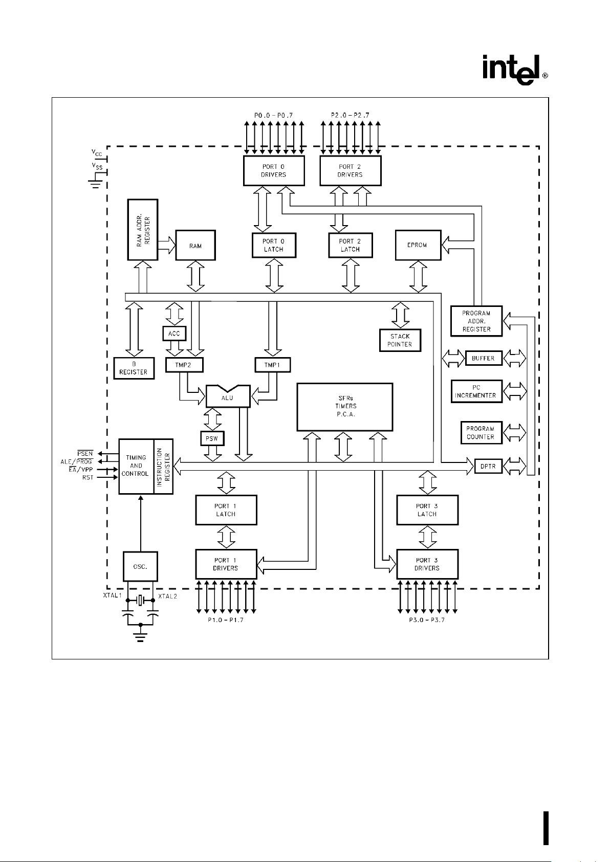
Figure 1. M80C51FB Block Diagram
2
Page 3
M80C51FB
DIP
271172–2
LCC/Gull Wing/J-Lead
271172–3
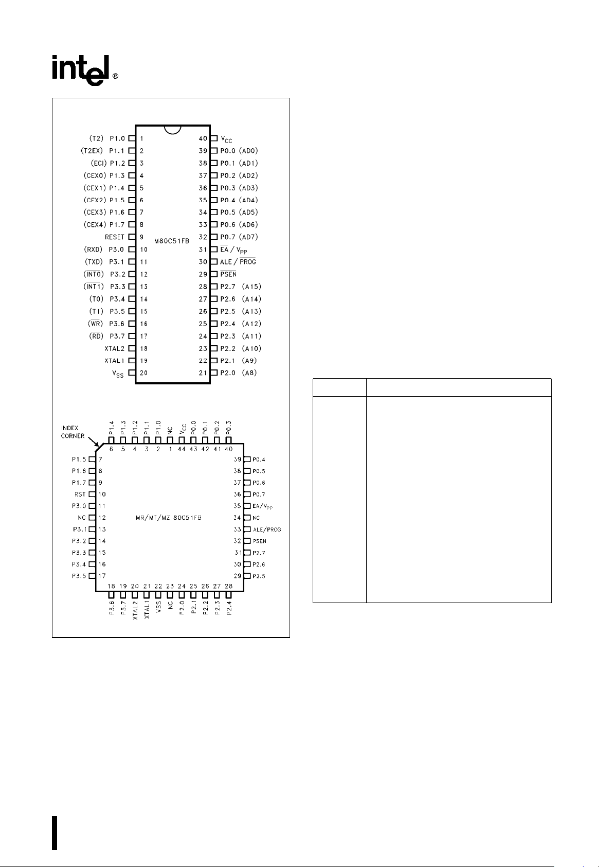
Figure 2. M80C51FB Pin Connections
PIN DESCRIPTIONS
VCC: Supply voltage.
V
SS
: Circuit ground.
Port 0: Port 0 is an 8-bit, open drain, bidirectional I/O
port. As an output port each pin can sink several LS
TTL inputs. Port 0 pins that have 1’s written to them
float, and in that state can be used as high-impedance inputs.
Port 0 is also the multiplexed low-order address and
data bus during accesses to external Program and
Data Memory. In this application it uses strong internal pullups when emitting1’s, and can source and
sink several LS TTL inputs.
Port 1: Port 1 is an 8-bit bidirectional I/O port with
internal pullups. The Port 1 output buffers can drive
LS TTL inputs. Port 1 pins that have 1’s written to
them are pulled high by the internal pullups, and in
that state can be used as inputs. As inputs, Port 1
pins that are externally being pulled low will source
current (I
IL
, on the data sheet) because of the inter-
nal pullups.
In addition, Port 1 serves the functions of the following special features of the M80C51FB:
Port Pin Alternate Function
P1.0 T2 (External Count Input to Timer/
Counter 2)
P1.1 T2EX (Timer/Counter 2 Capture/
Reload Trigger and Direction Control)
P1.2 ECI (External Count Input to the PCA)
P1.3 CEX0 (External I/O for Compare/
Capture Module 0)
P1.4 CEX1 (External I/O for Compare/
Capture Module 1)
P1.5 CEX2 (External I/O for Compare/
Capture Module 2)
P1.6 CEX3 (External I/O for Compare/
Capture Module 3)
P1.7 CEX4 (External I/O for Compare/
Capture Module 4)
Port 2: Port 2 is an 8-bit bidirectional I/O port with
internal pullups. The Port 2 output buffers can drive
LS TTL inputs. Port 2 pins that have 1’s written to
them are pulled high by the internal pullups, and in
that state can be used as inputs. As inputs, Port 2
pins that are externally being pulled low will source
current (I
IL
, on the data sheet) because of the inter-
nal pullups.
3
Page 4
M80C51FB
Port 2 emits the high-order address byte during
fetches from external Program Memory and during
accesses to external Data Memory that use 16-bit
addresses (MOVX
@
DPTR). In this application it
uses strong internal pullups when emitting 1’s. During accesses to external Data Memory that use 8-bit
addresses (MOVX
@
Ri), Port 2 emits the contents of
the P2 Special Function Register.
Port 3: Port 3 is an 8-bit bidirectional I/O port with
internal pullups. The Port 3 output buffers can drive
LS TTL inputs. Port 3 pins that have 1’s written to
them are pulled high by the internal pullups, and in
that state can be used as inputs. As inputs, Port 3
pins that are externally being pulled low will source
current (I
IL
, on the data sheet) because of the pull-
ups.
Port 3 also serves the functions of various special
features of the M8051 Family, as listed below:
Port Pin Alternate Function
P3.0 RXD (serial input port)
P3.1 TXD (serial output port)
P3.2 INT0 (external interrupt 0)
P3.3 INT1
(external interrupt 1)
P3.4 T0 (Timer 0 external input)
P3.5 T1 (Timer 1 external input)
P3.6 WR
(external data memory write strobe)
P3.7 RD
(external data memory read strobe)
RST: Reset input. A high on this pin for two machine
cycles while the oscillator is running resets the device. An internal pulldown resistor permits a poweron reset with only a capacitor connected to V
CC
.
ALE: Address Latch Enable output pulse for latching
the low byte of the address during accesses to external memory.
In normal operation ALE is emitted at a constant
rate of (/6 the oscillator frequency, and may be used
for external timing or clocking purposes. Note, however, that one ALE pulse is skipped during each access to external Data Memory.
PSEN
: Program Store Enable is the read strobe to
external Program Memory.
When the M80C51FB is executing code from external Program Memory, PSEN
is activated twice each
machine cycle, except that two PSEN
activations
are skipped during each access to external Data
Memory.
EA
: External Access enable. EA must be strapped to
VSS in order to enable the device to fetch code from
external Program Memory.
XTAL1: Input to the inverting oscillator amplifier.
XTAL2: Output from the inverting oscillator amplifier.
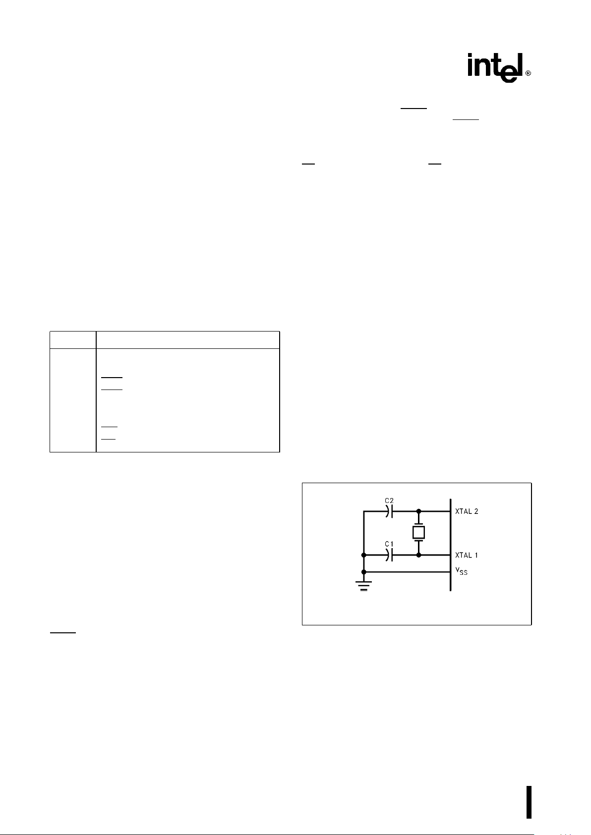
OSCILLATOR CHARACTERISTICS
XTAL1 and XTAL2 are the input and output, respectively, of an inverting amplifier which can be configured for use as an on-chip oscillator, as shown in
Figure 3. Either a quartz crystal or ceramic resonator
may be used. More detailed information concerning
the use of the on-chip oscillator is available in Application Note AP-155, ‘‘Oscillators for Microcontrollers.’’
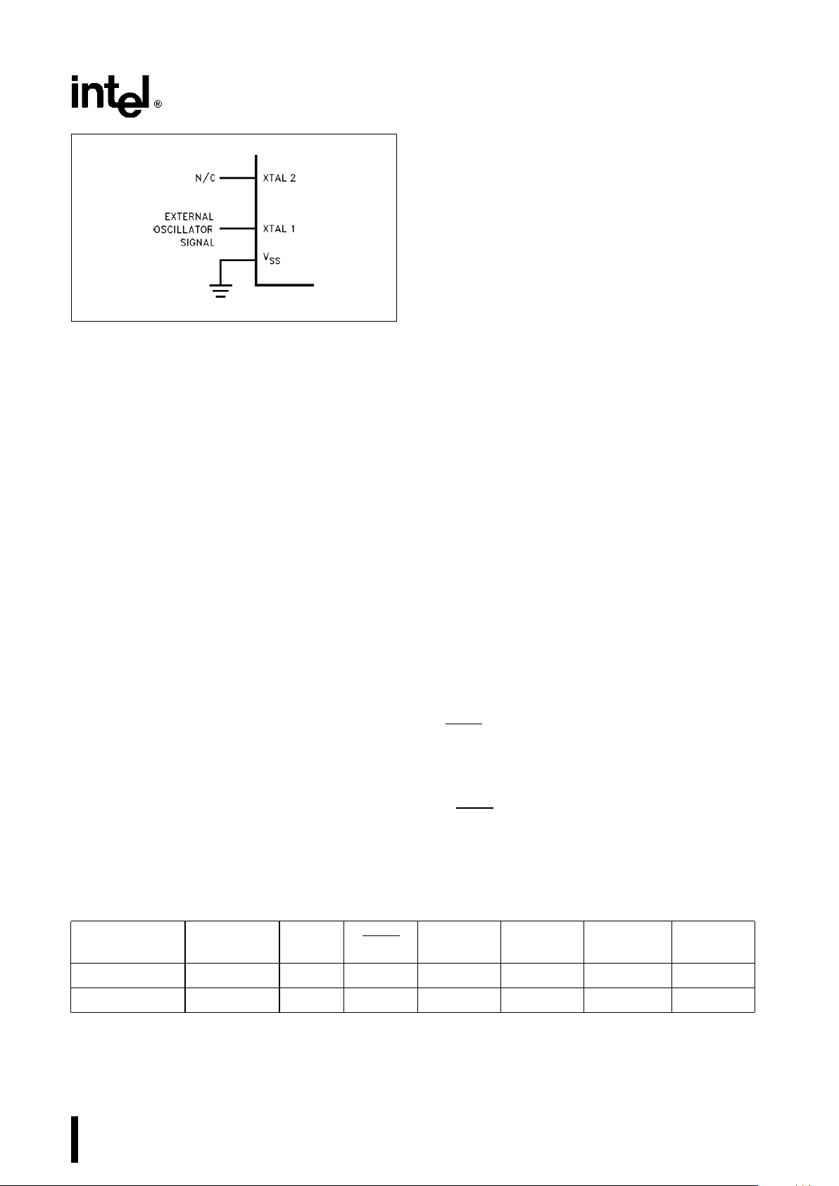
To drive the device from an external clock source,
XTAL1 should be driven, while XTAL2 floats, as
shown in Figure 4. There are no requirements on the
duty cycle of the external clock signal, since the input to the internal clocking circuitry is through a divide-by-two flip-flop, but minimum and maximum
high and low times specified on the data sheet must
be observed.
271172–4
C1, C2
e
30 pFg10 pF for Crystals
e
10 pF for Ceramic Resonators
Figure 3. Oscillator Connections
4
Page 5
M80C51FB
271172–5
Figure 4. External Clock Drive Configuration
IDLE MODE
The user’s software can invoke the Idle Mode. When
the microcontroller is in this mode, power consumption is reduced. The Special Function Registers and
the onboard RAM retain their values during Idle, but
the processor stops executing instructions. Idle
Mode will be exited if the chip is reset or if an enabled interrupt occurs. The PCA timer/counter can
optionally be left running or paused during Idle
Mode.
POWER DOWN MODE
To save even more power, a Power Down Mode can
be invoked by software. In this mode, the oscillator
is stopped and the instruction that invoked Power
Down is the last instruction executed. The on-chip
RAM and Special Function Registers retain their values until the Power Down Mode is terminated.
On the M80C51FB either a hardware reset or an
external interrupt can cause an exit from Power
Down. Reset redefines all the SFRs but does not
change the on-chip RAM. An external interrupt allows both the SFRs and on-chip RAM to retain their
values.
To properly terminate Power Down the reset or external interrupt should not be executed before V
CC
is
restored to its normal operating level and must be
held active long enough for the oscillator to restart
and stabilize (normally less than 10 ms).
With an external interrupt, INT0 and INT1 must be
enabled and configured as level-sensitive. Holding
the pin low restarts the oscillator but bringing the pin
back high completes the exit. Once the interrupt is
serviced, the next instruction to be executed after
RETI will be the one following the instruction that
puts the device into Power Down.
DESIGN CONSIDERATION
When the Idle Mode is terminated by a hardware
reset, the device normally resumes program execution, from where it left off, up to two machine cycles
before the internal reset algorithm takes control. Onchip hardware inhibits access to internal RAM in this
event, but access to the port pins is not inhibited. To
eliminate the possibility of an unexpected write when
Idle is terminated by reset, the instruction following
the one that invokes Idle should not be one that
writes to a port pin or to external memory.
ONCE MODE
The ONCE (‘‘On-Circuit Emulation’’) Mode facilitates
testing and debugging of systems using the
M80C51FB without the M80C51FB having to be removed from the circuit. The ONCE Mode is invoked
by:
1) Pull ALE low while the device is in reset and
PSEN
is high;
2) Hold ALE low as RST is deactivated.
While the device is in ONCE Mode, the Port 0 pins
go into a float state, and the other port pins and ALE
and PSEN
are weakly pulled high. The oscillator circuit remains active. While the M80C51FB is in this
mode, an emulator or test CPU can be used to drive
the circuit. Normal operation is restored when a normal reset is applied.
Table 1. Status of the External Pins during Idle and Power Down
Mode
Program
ALE PSEN PORT0 PORT1 PORT2 PORT3
Memory
Idle External 1 1 Float Data Address Data
Power Down External 0 0 Float Data Data Data
NOTE:
For more detailed information on the reduced power modes refer to current 8-Bit Embedded Controller Handbook, and
Application Note AP-255, ‘‘Designing with the M80C51BH.’’
5
Page 6
M80C51FB
ABSOLUTE MAXIMUM RATINGS*
Case Temperature
under Bias
(6)
ААААААААААААААААb55§Ctoa125§C
Storage Temperature ААААААААААb65§Ctoa150§C
Voltage on EA/VPPPin to VSSААААААА0V toa13.0V
Voltage on Any Other Pin to VSSÀÀb0.5V toa6.5V
Maximum IOLPer I/O Pin АААААААААААААААААА15 mA
Power DissipationАААААААААААААААААААААААААА1.5W
(based on PACKAGE heat transfer limitations, not
device power consumption)
NOTICE: This is a production data sheet. The specifications are subject to change without notice.
*
WARNING: Stressing the device beyond the ‘‘Absolute
Maximum Ratings’’ may cause permanent damage.
These are stress ratings only. Operation beyond the
‘‘Operating Conditions’’ is not recommended and extended exposure beyond the ‘‘Operating Conditions’’
may affect device reliability.
Operating Conditions
Symbol Description Min Max Unit
T
C
Case Temperature (Instant On)
b
55
a
125
§
C
V
CC
Digital Supply Voltage 4.0 6.0 V
f
OSC
Oscillator Frequency 3.5 16 MHz
D.C. CHARACTERISTICS: (Over Specified Operating Conditions)
Symbol Parameter Min Max Unit Test Conditions
V
IL
Input Low Voltage
b
0.5 0.2 V
CC
b
0.1 V
V
IH
Input High Voltage 0.2 V
CC
a
0.9 V
CC
a
0.5 V
(Except XTAL1, RST)
V
IH1
Input High Voltage (XTAL1, RST) 0.7 V
CC
V
CC
a
0.5 V
V
OL
Output Low Voltage
(5)
0.3 V I
OL
e
100 mA (Note 1)
(Ports 1, 2, and 3)
0.45 V I
OL
e
1.6 mA (Note 1)
1.0 V I
OL
e
3.5 mA (Notes 1, 4)
V
OL1
Output Low Voltage
(5)
0.3 V I
OL
e
200 mA (Note 1)
(Port 0, ALE, PSEN)
0.45 V I
OL
e
3.2 mA (Note 1)
1.0 V I
OL
e
7.0 mA (Note 1, 4)
V
OH
Output High Voltage V
CC
b
0.3 V I
OH
eb
10 mA
(Ports 1, 2, and 3)
V
CC
b
0.7 V I
OH
eb
30 mA
V
CC
b
1.5 V I
OH
eb
60 mA
6
Page 7

M80C51FB
D.C. CHARACTERISTICS: (Over Specified Operating Conditions) (Continued)
Symbol Parameter Min Max Unit Test Conditions
V
OH1
Output High Voltage V
CC
b
0.3 V I
OH
eb
200 mA (Note 2)
(Port 0 in External Bus Mode,
V
CC
b
0.7 V I
OH
eb
3.2 mA
ALE, PSEN)
V
CC
b
1.5 V I
OH
eb
7.0 mA (Note 4)
I
IL
Logical 0 Input Current
b
75 mAV
IN
e
0.45V
(Ports 1, 2, and 3)
I
LI
Input leakage Current (Port 0)
g
10 mA 0.45VkV
IN
k
V
CC
I
TL
Logical 1 to 0 Transition Current
b
750 mAV
IN
e
2V
(Ports 1, 2, and 3)
RRST RST Pulldown Resistor 40 225 KX
CIO Pin Capacitance 10 pF
@
1 MHz, 25§C
I
CC
Power Supply Current: (Note 3)
Active Mode
@
16 MHz 45 mA
Idle Mode
@
16 MHz 15 mA
Power Down Mode
@
16 MHz 130 mA
NOTES:
1. Capacitive loading on Ports 0 and 2 may cause spurious noise pulses to be superimposed on the V
OL
s of ALE and Ports
1 and 3. The noise is due to external bus capacitance discharging into the Port 0 and Port 2 pins when these pins make 1 to
0 transitions during bus operations. In applications where capacitance loading exceeds 100 pFs, the noise pulse on the ALE
signal may exceed 0.8V. In these cases, it may be desirable to qualify ALE with a Schmitt Trigger, or use an Address Latch
with a Schmitt Trigger Strobe input.
2. Capacitive loading on Ports 0 and 2 cause the V
OH
on ALE and PSEN to drop below the V
CC
b
0.3 specification when
the address lines are stabilizing.
3. See Figures 5 – 8 for load circuits. Minimum V
CC
for Power Down is 2V.
4. Care must be taken not to exceed the maximum allowable power dissipation.
5. Under steady state (non-transient) conditions, I
OL
must be externally limited as follows:
Maximum I
OL
per port pin: 10mA
Maximum I
OL
per 8-bit portÐ
Port 0: 26 mA
Ports 1, 2 and 3: 15 mA
Maximum total I
OL
for all output pins: 71 mA
If I
OL
exceeds the test condition, VOLmay exceed the related specification. Pins are not guaranteed to sink current greater
than the listed test conditions.
271172–6
All other pins disconnected
TCLCH
e
TCHCLe5ns
Figure 5. ICCLoad Circuit Active Mode
271172–7
All other pins disconnected
TCLCH
e
TCHCLe5ns
Figure 6. ICCLoad Circuit Idle Mode
7
Page 8

M80C51FB
271172–8
All other pins disconnected
Figure 7. ICCLoad Circuit Power Down Mode.
V
CC
e
2.0V to 5.5V.
271172–9
Figure 8. Clock Signal Waveform for ICCTests in Active and Idle Modes. TCLCHeTCHCLe5 ns.
EXPLANATION OF THE AC SYMBOLS
Each timing symbol has 5 characters. The first character is always a ‘T’ (stands for time). The other
characters, depending on their positions, stand for
the name of a signal or the logical status of that
signal. The following is a list of all the characters and
what they stand for.
A: Address
C: Clock
D: Input Data
H: Logic level HIGH
I: Instruction (program memory contents)
L: Logic level LOW, or ALE
P: PSEN
Q: Output Data
R: RD
signal
T: Time
V: Valid
W: WR
signal
X: No longer a valid logic level
Z: Float
For example,
TAVLL
e
Time from Address Valid to ALE Low
TLLPL
e
Time from ALE Low to PSEN Low
8
Page 9

M80C51FB
A.C. CHARACTERISTICS (Over Specified Operating Conditions)
EXTERNAL PROGRAM MEMORY CHARACTERISTICS
12 MHz 16 MHz Variable
Symbol Parameter Oscillator Oscillator Oscillator Unit
Min Max Min Max Min Max
1/TCLCL Oscillator Frequency
M80C51FB 3.5 12
MHz
M80C51FB-16 3.5 16
TLHLL ALE Pulse Width 127 85 2TCLCLb40 ns
TAVLL Address Valid to ALE Low 43 23 TCLCLb40 ns
TLLAX Address Hold After ALE Low 53 33 TCLCLb30 ns
TLLIV ALE Low to 234 150 4TCLCLb110 ns
Valid Instruction In
TLLPL ALE Low to PSEN
Low 53 33 TCLCL
b
30 ns
TPLPH PSEN Pulse Width 205 143 3TCLCLb45 ns
TPLIV PSEN Low to 145 83 3TCLCLb115 ns
Valid Instruction In
TPXIX Input Instruction Hold 0 0 0 ns
After PSEN
TPXIZ Input Instruction Float 59 38 TCLCLb25 ns
After PSEN
TAVIV Address to 312 208 5TCLCLb115 ns
Valid Instruction In
TPLAZ PSEN Low to Address Float 10 10 20 ns
TRLRH RD Pulse Width 400 275 6TCLCLb100 ns
TWLWH WR Pulse Width 400 275 6TCLCLb100 ns
TRLDV RD Low to Valid Data In 252 147.5 5TCLCLb175 ns
TRHDX Data Hold After RD 00 0 ns
TRHDZ Data Float After RD 107 65 2TCLCLb60 ns
TLLDV ALE Low to Valid Data In 517 350 8TCLCLb160 ns
TAVDV Address to Valid Data In 585 398 9TCLCLb175 ns
TLLWL ALE Low to RD or WR Low 200 300 138 238 3TCLCLb50 3TCLCLa50 ns
TAVWL Address Valid to WR Low 203 120 4TCLCLb130 ns
TQVWX Data Valid before WR 33 13 TCLCLb50 ns
TWHQX Data Hold after WR 33 13 TCLCLb50 ns
TQVWH Data Valid to WR High 433 288 7TCLCLb150 ns
TRLAZ RD Low to Address Float 0 0 0 ns
TWHLH RD or WR High to ALE High 43 123 23 103 TCLCLb40 TCLCLa40 ns
NOTE:
7. Case temperatures are ‘‘instant on’’.
9
Page 10

M80C51FB
EXTERNAL PROGRAM MEMORY READ CYCLE
271172–10
EXTERNAL DATA MEMORY READ CYCLE
271172–11
EXTERNAL DATA MEMORY WRITE CYCLE
271172–12
10
Page 11

M80C51FB
SERIAL PORT TIMING - SHIFT REGISTER MODE
Test Conditions:
(Over Specified Operating Conditions)
12 MHz 16 MHz Variable
Symbol Parameter Oscillator Oscillator Oscillator Units
Min Max Min Max Min Max
TXLXL Serial Port Clock Cycle Time 1 0.75 12TCLCL ms
TQVXH Output Data Setup to Clock 700 492 10TCLCLb133 ns
Rising Edge
TXHQX Output Data Hold after 50 8 2TCLCLb117 ns
Clock Rising Edge
TXHDX Input Data Hold After Clock 0 0 0 ns
Rising Edge
TXHDV Clock Rising Edge to Input 700 492 10TCLCLb133 ns
Data Valid
SHIFT REGISTER MODE TIMING WAVEFORMS
271172–13
11
Page 12
M80C51FB
EXTERNAL CLOCK DRIVE
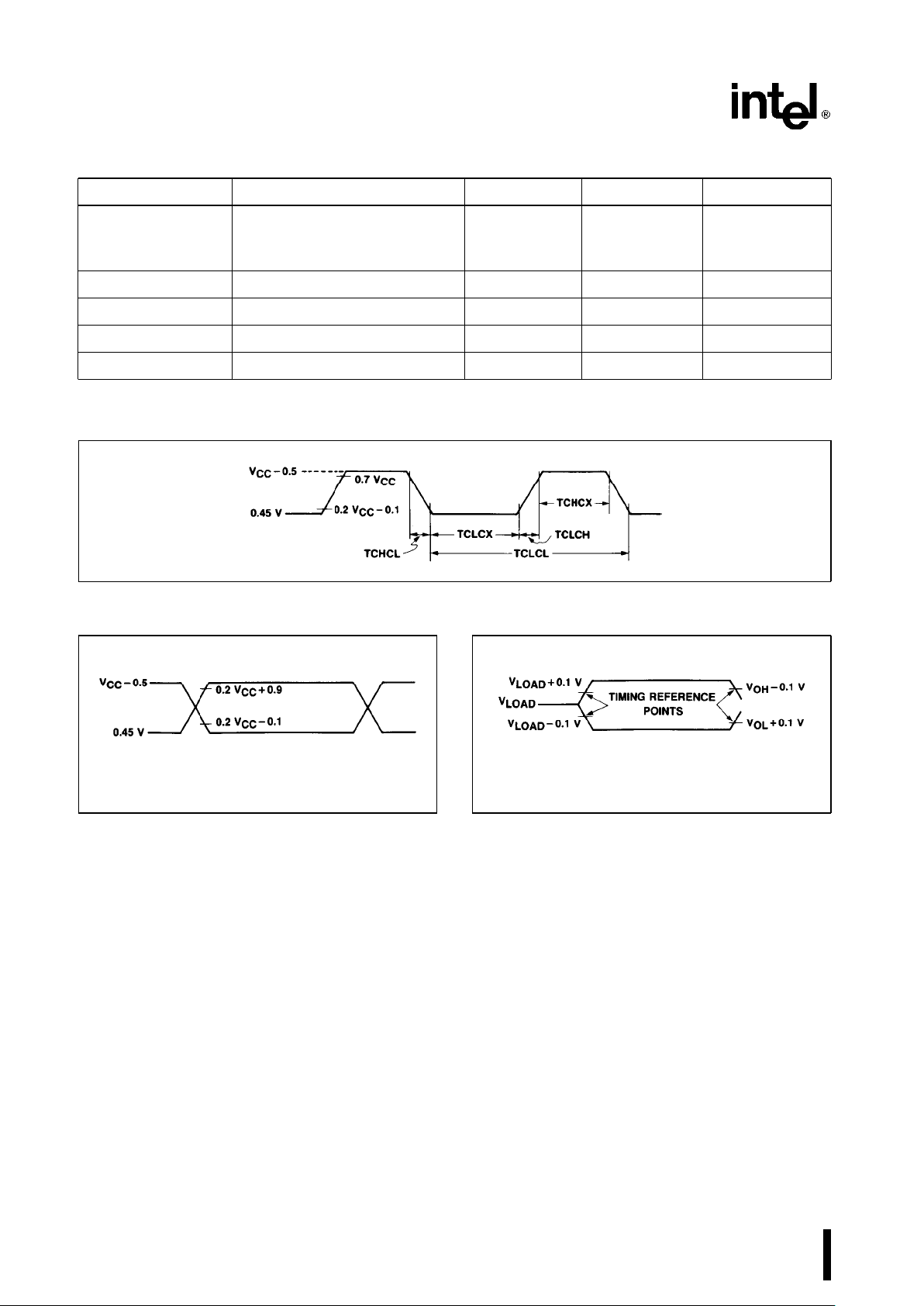
Symbol Parameter Min Max Units
1/TCLCL Oscillator Frequency
M80C51FB 3.5 12 MHz
M80C51FB-16 3.5 16
TCHCX High Time 20 ns
TCLCX Low Time 20 ns
TCLCH Rise Time 20 ns
TCHCL Fall Time 20 ns
EXTERNAL CLOCK DRIVE WAVEFORM
271172–14
A.C. TESTING INPUT
Input, Output Waveforms
271172–15
AC Inputs during testing are driven at V
CC
b
0.5V for a Logic ‘‘1’’
and 0.45V for a Logic ‘‘0’’. Timing measurements are made at V
IH
min for a Logic ‘‘1’’ and VILmax for a Logic ‘‘0’’.
Float Waveforms
271172–16
For timing purposes a port pin is no longer floating when a
100 mV change from load voltage occurs, and begins to float
when a 100 mV change from the loaded V
OH/VOL
level occurs.
I
OL/IOH
t
g
20 mA.
12
 Loading...