

Page 1
1
Motorola Small–Signal Transistors, FETs and Diodes Device Data
PNP Silicon
MAXIMUM RATINGS
Rating Symbol Value Unit
Collector–Emitter Voltage V
CEO
–40 Vdc
Emitter–Base Voltage V
EBO
–4.0 Vdc
Collector Current — Continuous I
C
–100 mAdc
Total Device Dissipation @ TA = 25°C
Derate above 25°C
P
D
625
5.0
mW
mW/°C
Total Device Dissipation @ TC = 25°C
Derate above 25°C
P
D
1.5
12
Watts
mW/°C
Operating and Storage Junction
Temperature Range
TJ, T
stg
–55 to +150 °C
THERMAL CHARACTERISTICS
Characteristic Symbol Max Unit
Thermal Resistance, Junction to Ambient
R
q
JA
200 °C/W
Thermal Resistance, Junction to Case
R
q
JC
83.3 °C/W
ELECTRICAL CHARACTERISTICS (T
A
= 25°C unless otherwise noted)
Characteristic
Symbol Min Max Unit
OFF CHARACTERISTICS
Collector–Emitter Breakdown Voltage
(1)
(IC = –1.0 mAdc, IB = 0)
V
(BR)CEO
–40 — Vdc
Emitter–Base Breakdown Voltage
(IE = –100 µAdc, IC = 0)
V
(BR)EBO
–4.0 — Vdc
Collector Cutoff Current
(VCB = –30 Vdc, IE = 0)
I
CBO
— –100 nAdc
1. Pulse Test: Pulse Width v 300 ms; Duty Cycle v 2.0%.
Order this document
by MPSA70/D
SEMICONDUCTOR TECHNICAL DATA
CASE 29–04, STYLE 1
TO–92 (TO–226AA)
1
2
3
Motorola, Inc. 1996
COLLECTOR
3
2
BASE
1
EMITTER
Page 2
MPSA70
2
Motorola Small–Signal Transistors, FETs and Diodes Device Data
ELECTRICAL CHARACTERISTICS
(TA = 25°C unless otherwise noted) (Continued)
Characteristic
Symbol Min Max Unit
ON CHARACTERISTICS
DC Current Gain
(IC = –5.0 mAdc, VCE = –10 Vdc)
h
FE
40 400 —
Collector–Emitter Saturation Voltage
(IC = –10 mAdc, IB = –1.0 mAdc)
V
CE(sat)
— –0.25 Vdc
SMALL–SIGNAL CHARACTERISTICS
Current–Gain — Bandwidth Product
(IC = –5.0 mAdc, VCE = –10 Vdc, f = 100 MHz)
f
T
125 — MHz
Output Capacitance
(VCB = –10 Vdc, IE = 0, f = 1.0 MHz)
C
obo
— 4.0 pF
Page 3
MPSA70
3
Motorola Small–Signal Transistors, FETs and Diodes Device Data
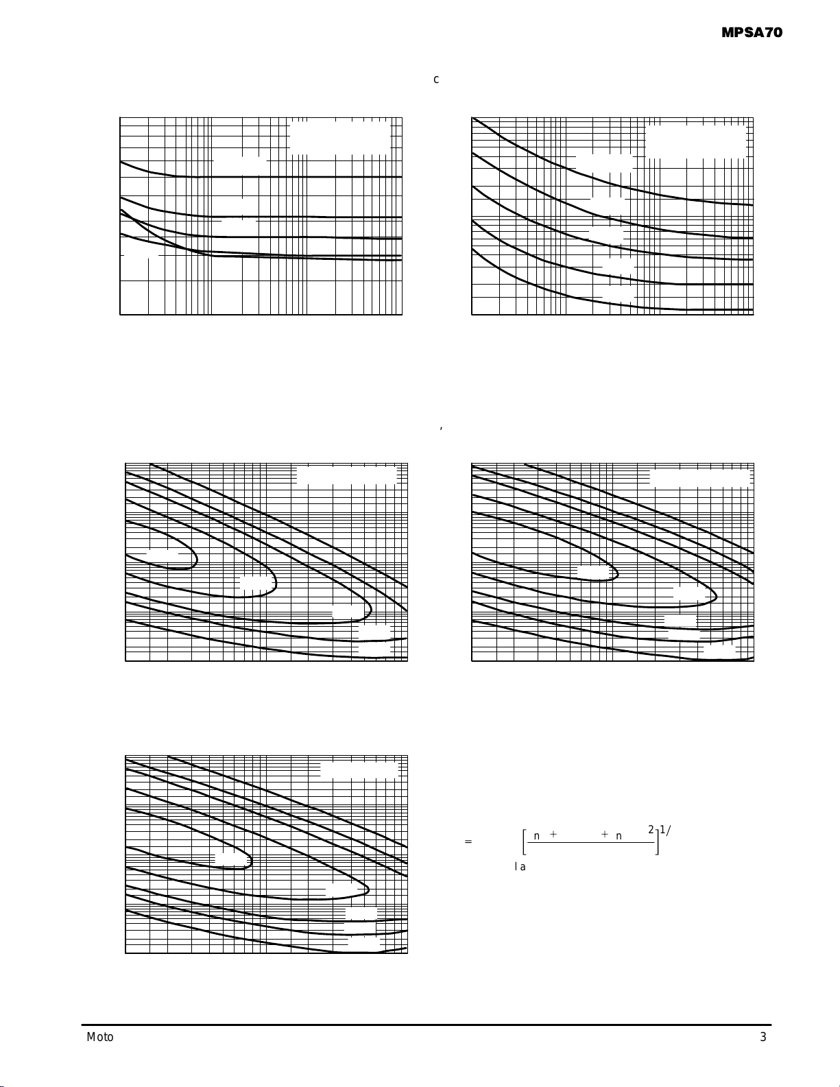
TYPICAL NOISE CHARACTERISTICS
(VCE = –ā5.0 Vdc, TA = 25°C)
Figure 1. Noise Voltage
f, FREQUENCY (Hz)
5.0
7.0
10
3.0
Figure 2. Noise Current
f, FREQUENCY (Hz)
1.0
10 20 50 100 200 500 1.0 k 2.0 k 5.0 k 10 k
1.0
7.0
5.0
3.0
2.0
1.0
0.7
0.5
0.3
0.1
BANDWIDTH = 1.0 Hz
RS
≈
0
IC = 10 µA
100 µA
e
n
, NOISE VOLTAGE (nV)
I
n
, NOISE CURRENT (pA)
30 µA
BANDWIDTH = 1.0 Hz
RS
≈ ∞
IC = 1.0 mA
300 µA
100 µA
30 µA
10 µA
10 20 50 100 200 500 1.0 k 2.0 k 5.0 k 10 k
2.0
1.0 mA
0.2
300 µA
NOISE FIGURE CONTOURS
(VCE = –ā5.0 Vdc, TA = 25°C)
500 k
100
200
500
1.0 k
10 k
5.0 k
20 k
50 k
100 k
200 k
2.0 k
1.0 M
500 k
100
200
500
1.0 k
10 k
5.0 k
20 k
50 k
100 k
200 k
2.0 k
1.0 M
Figure 3. Narrow Band, 100 Hz
IC, COLLECTOR CURRENT (µA)
Figure 4. Narrow Band, 1.0 kHz
IC, COLLECTOR CURRENT (µA)
10
0.5 dB
BANDWIDTH = 1.0 Hz
R
S
, SOURCE RESISTANCE (OHMS)
R
S
, SOURCE RESISTANCE (OHMS)
Figure 5. Wideband
IC, COLLECTOR CURRENT (µA)
10
10 Hz to 15.7 kHz
R
S
, SOURCE RESISTANCE (OHMS)
Noise Figure is Defined as:
NF+20 log
10
ƪ
e
n
2
)
4KTRS)
I
n
2
R
S
2
4KTR
S
ƫ
1ń2
= Noise Voltage of the T ransistor referred to the input. (Figure 3)
= Noise Current of the Transistor referred to the input. (Figure 4)
= Boltzman’s Constant (1.38 x 10
–23
j/°K)
= Temperature of the Source Resistance (°K)
= Source Resistance (Ohms)
e
n
I
n
K
T
R
S
1.0 dB
2.0 dB
3.0 dB
20 30 50 70 100 200 300 500 700 1.0 k 10 20 30 50 70 100 200 300 500 700 1.0 k
500 k
100
200
500
1.0 k
10 k
5.0 k
20 k
50 k
100 k
200 k
2.0 k
1.0 M
20 30 50 70 100 200 300 500 700 1.0 k
BANDWIDTH = 1.0 Hz
5.0 dB
0.5 dB
1.0 dB
2.0 dB
3.0 dB
5.0 dB
0.5 dB
1.0 dB
2.0 dB
3.0 dB
5.0 dB
Page 4

MPSA70
4
Motorola Small–Signal Transistors, FETs and Diodes Device Data
TYPICAL STATIC CHARACTERISTICS
Figure 6. DC Current Gain
IC, COLLECTOR CURRENT (mA)
400
0.003
h , DC CURRENT GAIN
FE
TJ = 125°C
–55°C
25°C
VCE = 1.0 V
VCE = 10 V
Figure 7. Collector Saturation Region
IC, COLLECTOR CURRENT (mA)
1.4
Figure 8. Collector Characteristics
IC, COLLECTOR CURRENT (mA)
V, VOLTAGE (VOLTS)
1.0 2.0 5.0 10 20
50
1.6
100
TJ = 25°C
V
BE(sat)
@ IC/IB = 10
V
CE(sat)
@ IC/IB = 10
V
BE(on)
@ VCE = 1.0 V
*
q
VC
for V
CE(sat)
q
VB
for V
BE
0.1 0.2 0.5
MPSA70
Figure 9. “On” Voltages
IB, BASE CURRENT (mA)
0.4
0.6
0.8
1.0
0.2
0
V
CE
, COLLECTOR–EMITTER VOLTAGE (VOLTS)
0.002
TA = 25°C
MPSA70
IC = 1.0 mA 10 mA 100 mA
Figure 10. Temperature Coefficients
50 mA
VCE, COLLECTOR–EMITTER VOLTAGE (VOLTS)
40
60
80
100
20
0
0
I
C
, COLLECTOR CURRENT (mA)
TA = 25°C
PULSE WIDTH = 300
µ
s
DUTY CYCLE
≤
2.0%
IB = 400 µA
350 µA
300 µA
250 µA
200 µA
*APPLIES for IC/IB ≤ hFE/2
25°C to 125°C
–55°C to 25°C
25°C to 125°C
–55°C to 25°C
40
60
0.005 0.01 0.02 0.03 0.05 0.07 0.1 0.2 0.3 0.5 0.7 1.0
2.0
3.0
5.0 7.0 10 20 30 50 70 100
0.005 0.01 0.02 0.05 0.1 0.2 0.5 1.0 2.0 5.0 10 20 5.0 10 15 20 25 30 35 40
1.2
1.0
0.8
0.6
0.4
0.2
0
2.4
0.8
0
1.6
0.8
1.0 2.0 5.0 10 20
50
100
0.1 0.2 0.5
200
100
80
V
, TEMPERATURE COEFFICIENTS (mV/ C)
°θ
150 µA
100 µA
50 µA
Page 5

MPSA70
5
Motorola Small–Signal Transistors, FETs and Diodes Device Data
TYPICAL DYNAMIC CHARACTERISTICS
C, CAPACITANCE (pF)
Figure 11. Turn–On Time
IC, COLLECTOR CURRENT (mA)
500
Figure 12. Turn–Off Time
IC, COLLECTOR CURRENT (mA)
2.0 5.0 10
20 30 50
1000
Figure 13. Current–Gain — Bandwidth Product
IC, COLLECTOR CURRENT (mA)
Figure 14. Capacitance
VR, REVERSE VOLTAGE (VOLTS)
Figure 15. Input Impedance
IC, COLLECTOR CURRENT (mA)
Figure 16. Output Admittance
IC, COLLECTOR CURRENT (mA)
3.01.0
500
0.5
10
t, TIME (ns)
t, TIME (ns)
f , CURRENT–GAIN — BANDWIDTH PRODUCT (MHz)
T
h , OUTPUT ADMITTANCE ( mhos)
oe
m
h
ie
, INPUT IMPEDANCE (k )
Ω
5.0
7.0
10
20
30
50
70
100
300
7.0
70 100
VCC = 3.0 V
IC/IB = 10
TJ = 25°C
td @ V
BE(off)
= 0.5 V
t
r
10
20
30
50
70
100
200
300
500
700
–
ā
2.0
–1.0
VCC = –ā3.0 V
IC/IB = 10
IB1 = I
B2
TJ = 25
°
C
t
s
t
f
50
70
100
200
300
0.7 1.0 2.0 3.0 5.0 7.0 10 20 30 50
TJ = 25°C
VCE = 20 V
5.0 V
1.0
2.0
3.0
5.0
7.0
0.1 0.2 0.5 1.0 2.0 5.0 10 20 500.05
C
ib
C
ob
2.0 5.0 10
20 50
1.0
0.2
100
0.3
0.5
0.7
1.0
2.0
3.0
5.0
7.0
10
20
0.1 0.2 0.5
VCE = –10 Vdc
f = 1.0 kHz
TA = 25°C
2.0 5.0 10
20 50
1.0
2.0
100
3.0
5.0
7.0
10
20
30
50
70
100
200
0.1 0.2 0.5
VCE = 10 Vdc
f = 1.0 kHz
TA = 25°C
200
–ā3.0
–
ā
5.0 –ā7.0
–
ā
20
–10
–ā30
–
ā
50 –ā70
–100
TJ = 25°C
MPSA70
hfe
≈
200
@ IC = –1.0 mA
MPSA70
hfe
≈
200
@ IC = 1.0 mA
Page 6

MPSA70
6
Motorola Small–Signal Transistors, FETs and Diodes Device Data
Figure 17. Thermal Response
t, TIME (ms)
1.0
0.01
r(t) TRANSIENT THERMAL RESISTANCE
(NORMALIZED)
0.01
0.02
0.03
0.05
0.07
0.1
0.2
0.3
0.5
0.7
0.02 0.05 0.1 0.2 0.5 1.0 2.0 5.0 10 20 50 100 200 500 1.0 k 2.0 k 5.0 k 10 k 20 k
50 k
100 k
D = 0.5
0.2
0.1
0.05
0.02
0.01
SINGLE PULSE
DUTY CYCLE, D = t1/t
2
D CURVES APPLY FOR POWER
PULSE TRAIN SHOWN
READ TIME AT t1 (SEE AN–569)
Z
θ
JA(t)
= r(t)
•
R
θ
JA
T
J(pk)
– TA = P
(pk)
Z
θ
JA(t)
t
1
t
2
P
(pk)
FIGURE 19
Figure 18. Active–Region Safe Operating Area
TJ, JUNCTION TEMPERATURE (°C)
10
4
–4
0
I
C
, COLLECTOR CURRENT (nA)
Figure 19. Typical Collector Leakage Current
VCE, COLLECTOR–EMITTER VOLTAGE (VOLTS)
400
2.0
I
C
, COLLECTOR CURRENT (mA)
DESIGN NOTE: USE OF THERMAL RESPONSE DATA
A train of periodical power pulses can be represented by the model
as shown in Figure 19. Using the model and the device thermal
response the normalized effective transient thermal resistance of
Figure 17 was calculated for various duty cycles.
To find Z
θJA(t)
, multiply the value obtained from Figure 17 by the
steady state value R
θJA
.
Example:
Dissipating 2.0 watts peak under the following conditions:
t1 = 1.0 ms, t2 = 5.0 ms (D = 0.2)
Using Figure 17 at a pulse width of 1.0 ms and D = 0.2, the reading of
r(t) is 0.22.
The peak rise in junction temperature is therefore
∆T = r(t) x P
(pk)
x R
θJA
= 0.22 x 2.0 x 200 = 88°C.
For more information, see AN–569.
The safe operating area curves indicate IC–VCE limits of t he
transistor that must be observed for reliable operation. Collector load
lines for specific circuits must fall below the limits indicated by the
applicable curve.
The data of Figure 18 is based upon T
J(pk)
= 150°C; TC or TA is
variable depending upon conditions. Pulse curves are valid for duty
cycles to 10% provided T
J(pk)
≤ 150°C. T
J(pk)
may be calculated from
the data in Figure 17. At high case or ambient temperatures, thermal
limitations will reduce the power than can be handled to values less
than the limitations imposed by second breakdown.
10
–2
10
–1
10
0
10
1
10
2
10
3
–200 +20 +40 + 60 +80 +100 +120 +140 +160
VCC = 30 V
I
CEO
I
CBO
AND
I
CEX
@ V
BE(off)
= 3.0 V
TA = 25°C
CURRENT LIMIT
THERMAL LIMIT
SECOND BREAKDOWN LIMIT
1.0 ms
10 µs
TC = 25°C
1.0 s
dc
dc
4.0
6.0
10
20
40
60
100
200
4.0 6.0 8.0 10 20
40
TJ = 150°C
100 µs
Page 7

MPSA70
7
Motorola Small–Signal Transistors, FETs and Diodes Device Data
PACKAGE DIMENSIONS
R
A
P
J
L
F
B
K
G
H
SECTION X–X
C
V
D
N
N
X X
SEATING
PLANE
DIM MIN MAX MIN MAX
MILLIMETERSINCHES
A 0.175 0.205 4.45 5.20
B 0.170 0.210 4.32 5.33
C 0.125 0.165 3.18 4.19
D 0.016 0.022 0.41 0.55
F 0.016 0.019 0.41 0.48
G 0.045 0.055 1.15 1.39
H 0.095 0.105 2.42 2.66
J 0.015 0.020 0.39 0.50
K 0.500 ––– 12.70 –––
L 0.250 ––– 6.35 –––
N 0.080 0.105 2.04 2.66
P ––– 0.100 ––– 2.54
R 0.115 ––– 2.93 –––
V 0.135 ––– 3.43 –––
1
STYLE 1:
PIN 1. EMITTER
2. BASE
3. COLLECTOR
CASE 029–04
(TO–226AA)
ISSUE AD
NOTES:
1. DIMENSIONING AND TOLERANCING PER ANSI
Y14.5M, 1982.
2. CONTROLLING DIMENSION: INCH.
3. CONTOUR OF PACKAGE BEYOND DIMENSION R
IS UNCONTROLLED.
4. DIMENSION F APPLIES BETWEEN P AND L.
DIMENSION D AND J APPLY BETWEEN L AND K
MINIMUM. LEAD DIMENSION IS UNCONTROLLED
IN P AND BEYOND DIMENSION K MINIMUM.
Page 8

MPSA70
8
Motorola Small–Signal Transistors, FETs and Diodes Device Data
Motorola reserves the right to make changes without further notice to any products herein. Motorola makes no warranty , representation or guarantee regarding
the suitability of its products for any particular purpose, nor does Motorola assume any liability arising out of the application or use of any product or circuit, and
specifically disclaims any and all liability , including without limitation consequential or incidental damages. “Typical” parameters which may be provided in Motorola
data sheets and/or specifications can and do vary in different applications and actual performance may vary over time. All operating parameters, including “Typicals”
must be validated for each customer application by customer’s technical experts. Motorola does not convey any license under its patent rights nor the rights of
others. Motorola products are not designed, intended, or authorized for use as components in systems intended for surgical implant into the body, or other
applications intended to support or sustain life, or for any other application in which the failure of the Motorola product could create a situation where personal injury
or death may occur. Should Buyer purchase or use Motorola products for any such unintended or unauthorized application, Buyer shall indemnify and hold Motorola
and its officers, employees, subsidiaries, affiliates, and distributors harmless against all claims, costs, damages, and expenses, and reasonable attorney fees
arising out of, directly or indirectly, any claim of personal injury or death associated with such unintended or unauthorized use, even if such claim alleges that
Motorola was negligent regarding the design or manufacture of the part. Motorola and are registered trademarks of Motorola, Inc. Motorola, Inc. is an Equal
Opportunity/Affirmative Action Employer.
How to reach us:
USA/EUROPE/Locations Not Listed: Motorola Literature Distribution; JAPAN: Nippon Motorola Ltd.; Tatsumi–SPD–JLDC, 6F Seibu–Butsuryu–Center,
P.O. Box 20912; Phoenix, Arizona 85036. 1–800–441–2447 or 602–303–5454 3–14–2 Tatsumi Koto–Ku, Tokyo 135, Japan. 03–81–3521–8315
MFAX: RMFAX0@email.sps.mot.com – TOUCHTONE 602–244–6609 ASIA/PACIFIC: Motorola Semiconductors H.K. Ltd.; 8B Tai Ping Industrial Park,
INTERNET: http://Design–NET.com 51 Ting Kok Road, Tai Po, N.T., Hong Kong. 852–26629298
MPSA70/D
*MPSA70/D*
◊
 Loading...