

Page 1
查询MPS2907ARLRA供应商
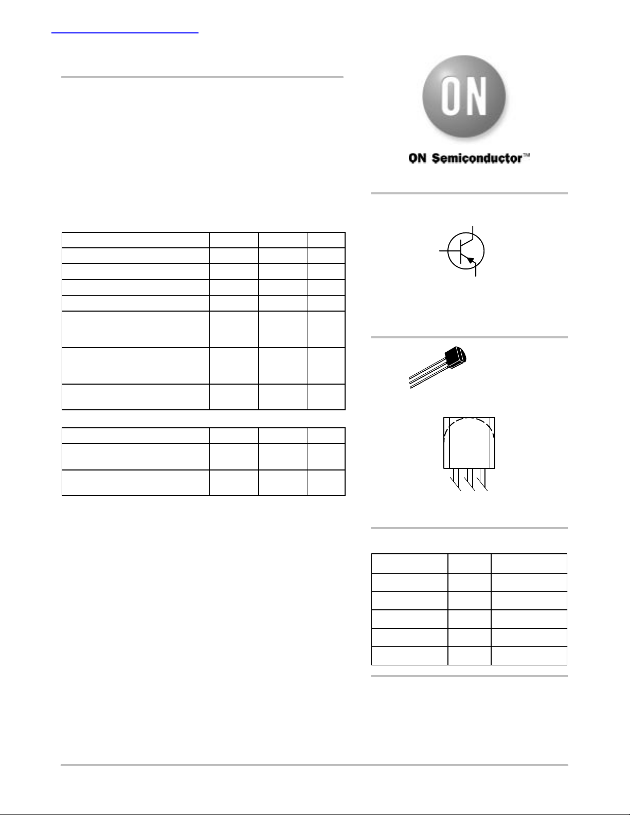
MPS2907A
Preferred Device
General Purpose
Transistors
PNP Silicon
MAXIMUM RATINGS
Rating Symbol Value Unit
Collector–Emitter Voltage V
Collector–Base Voltage V
Emitter–Base Voltage V
Collector Current – Continuous I
Total Device Dissipation
@ TA = 25°C
Derate above 25°C
Total Device Dissipation
@ TC = 25°C
Derate above 25°C
Operating and Storage Junction
Temperature Range
THERMAL CHARACTERISTICS
Characteristic Symbol Max Unit
Thermal Resistance,
Junction to Ambient
Thermal Resistance,
Junction to Case
CEO
CBO
EBO
P
P
TJ, T
R
θJA
R
θJC
http://onsemi.com
COLLECTOR
3
–60 Vdc
–60 Vdc
–5.0 Vdc
C
D
D
stg
–600 mAdc
625
5.0
1.5
12
–55 to
+150
200 °C/W
83.3 °C/W
mW
mW/°C
Watts
mW/°C
°C
2
BASE
EMITTER
STYLE 1
1
2
3
STYLES 1, 14
MARKING DIAGRAMS
MPS2
907A
YWW
Y = Year
WW = Work Week
1
TO–92
CASE 29
Semiconductor Components Industries, LLC, 2001
October, 2001 – Rev. 0
ORDERING INFORMATION
Device Package Shipping
MPS2907A TO–92 5000 Units/Box
MPS2907ARLRA TO–92 2000/Tape & Reel
MPS2907ARLRE TO–92 2000/Ammo Pack
MPS2907ARLRM TO–92 2000/Ammo Pack
MPS2907ARLRP TO–92 2000/Ammo Pack
Preferred devices are recommended choices for future use
and best overall value.
1 Publication Order Number:
MPS2907A/D
Page 2
MPS2907A
CC C
CC C
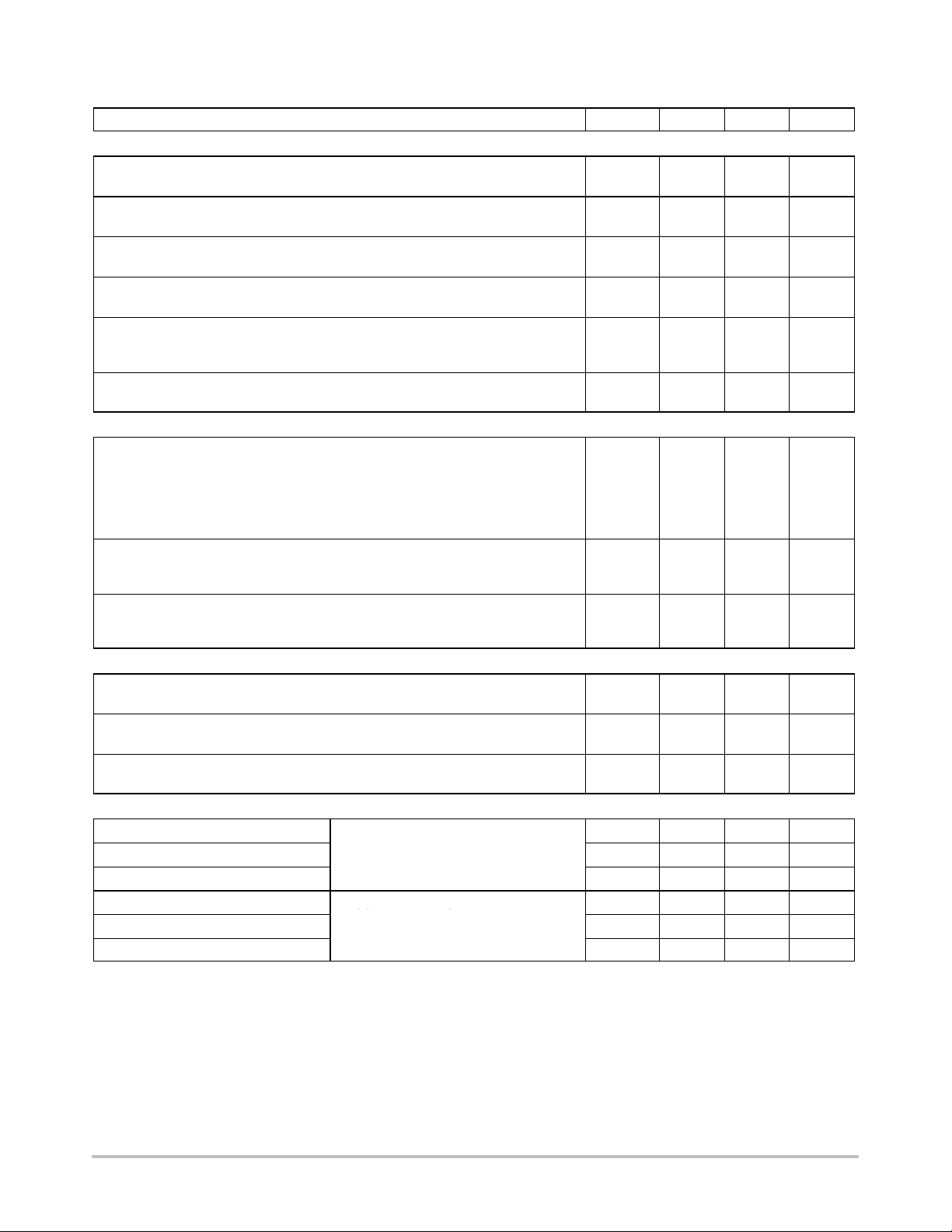
ELECTRICAL CHARACTERISTICS (T
Characteristic Symbol Min Max Unit
= 25°C unless otherwise noted)
A
OFF CHARACTERISTICS
Collector–Emitter Breakdown Voltage (Note 1.)
(IC = –10 mAdc, IB = 0)
Collector–Base Breakdown Voltage
(IC = –10 Adc, IE = 0)
Emitter–Base Breakdown Voltage
(IE = –10 Adc, IC = 0)
Collector Cutoff Current
(VCE = –30 Vdc, V
Collector Cutoff Current
(VCB = –50 Vdc, IE = 0)
(VCB = –50 Vdc, IE = 0, TA = 150°C)
Base Current
(VCE = –30 Vdc, V
EB(off)
EB(off)
= –0.5 Vdc)
= –0.5 Vdc)
ON CHARACTERISTICS
DC Current Gain
(IC = –0.1 mAdc, VCE = –10 Vdc)
(IC = –1.0 mAdc, VCE = –10 Vdc)
(IC = –10 mAdc, VCE = –10 Vdc)
(IC = –150 mAdc, VCE = –10 Vdc) (Note 1.)
(IC = –500 mAdc, VCE = –10 Vdc) (Note 1.)
Collector–Emitter Saturation Voltage (Note 1.)
(IC = –150 mAdc, IB = –15 mAdc)
(IC = –500 mAdc, IB = –50 mAdc)
Base–Emitter Saturation Voltage (Note 1.)
(IC = –150 mAdc, IB = –15 mAdc)
(IC = –500 mAdc, IB = –50 mAdc)
SMALL–SIGNAL CHARACTERISTICS
Current–Gain – Bandwidth Product (Notes 1. and 2.),
(IC = –50 mAdc, VCE = –20 Vdc, f = 100 MHz)
Output Capacitance
(VCB = –10 Vdc, IE = 0, f = 1.0 MHz)
Input Capacitance
(VEB = –2.0 Vdc, IC = 0, f = 1.0 MHz)
SWITCHING CHARACTERISTICS
Turn–On T ime
Delay Time
Rise Time t
Turn–Off Time
Storage Time
Fall Time t
1. Pulse Test: Pulse Width 300 s, Duty Cycle 2%.
2. fT is defined as the frequency at which |hfe| extrapolates to unity.
(VCC = –30 Vdc, IC = –150 mAdc,
IB1 = –15 mAdc) (Figures 1 and 5)
(VCC = –6.0 Vdc, IC = –150 mAdc,
IB1 = IB2 = 15 mAdc) (Figure 2)
V
(BR)CEO
V
(BR)CBO
V
(BR)EBO
I
CEX
I
CBO
I
B
h
FE
V
CE(sat)
V
BE(sat)
f
T
C
obo
C
ibo
t
on
t
d
r
t
off
t
s
f
–60 –
–60 – Vdc
–5.0 – Vdc
– –50 nAdc
–
–
– –50 nAdc
75
100
100
100
50
–
–
–
–
200 – MHz
– 8.0 pF
– 30 pF
– 45 ns
– 10 ns
– 40 ns
– 100 ns
– 80 ns
– 30 ns
–0.01
–10
–
–
–
300
–
–0.4
–1.6
–1.3
–2.6
Vdc
µAdc
–
Vdc
Vdc
http://onsemi.com
2
Page 3
MPS2907A
INPUT
Z
= 50 Ω
o
PRF = 150 PPS
RISE TIME ≤ 2.0 ns
P.W. < 200 ns
0
-16 V
200 ns
-30 V
200
1.0 k
50
TO OSCILLOSCOPE
RISE TIME ≤ 5.0 ns
INPUT
Z
= 50 Ω
o
PRF = 150 PPS
RISE TIME ≤ 2.0 ns
P.W. < 200 ns
0
-30 V
200 ns
+15 V -6.0 V
1.0 k
50
1.0 k 37
TO OSCILLOSCOPE
RISE TIME ≤ 5.0 ns
1N916
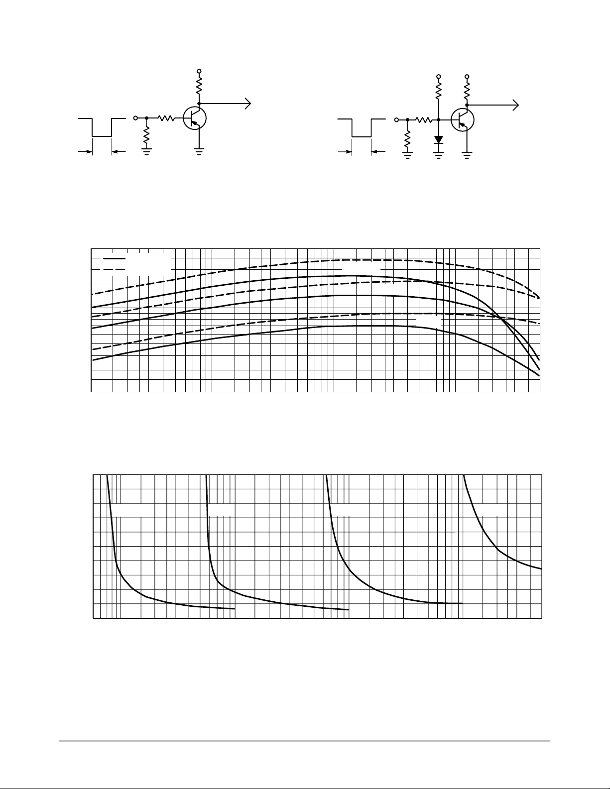
Figure 1. Delay and Rise Time Test Circuit Figure 2. Storage and Fall Time Test Circuit
TYPICAL CHARACTERISTICS
3.0
2.0
1.0
0.7
0.5
, NORMALIZED CURRENT GAIN
FE
0.3
h
VCE = -1.0 V
VCE = -10 V
T
= 125°C
J
25°C
-55°C
V , COLLECTOR-EMITTER VOLTAGE (VOLTS)
CE
0.2
-1.0
-0.8
-0.6
-0.4
-0.2
-0.005
-0.1
0
-0.2 -0.3 -0.5 -0.7 -1.0 -2.0 -3.0 -5.0 -7.0 -10 -20 -30 -50 -70 -100 -200 -300 -500
IC, COLLECTOR CURRENT (mA)
Figure 3. DC Current Gain
IC = -1.0 mA
-0.01
-10 mA
-0.02 -0.03 -0.05 -0.07 -0.1 -0.2 -0.3 -0.5 -0.7 -1.0
IB, BASE CURRENT (mA)
-100 mA
-2.0
-3.0
-5.0 -7.0 -10 -20
-500 mA
-30
Figure 4. Collector Saturation Region
-50
http://onsemi.com
3
Page 4

MPS2907A
TYPICAL CHARACTERISTICS
300
200
t
100
70
50
30
20
t, TIME (ns)
td @ V
10
7.0
5.0
3.0
-5.0
-7.0 -10 -20 -30 -50 -70 -100 -200 -300 -500
r
= 0 V
BE(off)
IC, COLLECTOR CURRENT
VCC = -30 V
IC/IB = 10
T
J
Figure 5. Turn–On Time
TYPICAL SMALL–SIGNAL CHARACTERISTICS
= 25°C
t, TIME (ns)
2.0 V
NOISE FIGURE
VCE = 10 Vdc, TA = 25°C
500
300
200
100
70
50
30
20
10
7.0
5.0
-7.0 -10 -20 -30 -50 -70 -100 -200 -300 -500
-5.0
t
f
t′
= ts - 1/8 t
s
IC, COLLECTOR CURRENT (mA)
f
VCC = -30 V
IC/IB = 10
IB1 = I
T
= 25°C
J
Figure 6. Turn–Off Time
B2
10
8.0
6.0
4.0
NF, NOISE FIGURE (dB)
2.0
0
0.01
0.02 0.05 0.1 0.2 0.5 1.0 2.0 5.0 10 20 50 100
IC = -1.0 mA, R
-500 µA, Rs = 560 Ω
-50 µA, Rs = 2.7 kΩ
-100 µA, Rs = 1.6 kΩ
f, FREQUENCY (kHz)
= 430 Ω
s
Rs = OPTIMUM SOURCE RESISTANCE
Figure 7. Frequency Effects
10
f = 1.0 kHz
8.0
6.0
4.0
NF, NOISE FIGURE (dB)
2.0
0
50 100 200 500 1.0 k 2.0 k 5.0 k 10 k 20 k 50 k
I
= -50 µA
C
-100 µA
-500 µA
-1.0 mA
Rs, SOURCE RESISTANCE (OHMS)
Figure 8. Source Resistance Effects
http://onsemi.com
4
Page 5

MPS2907A
)
TYPICAL SMALL–SIGNAL CHARACTERISTICS
NOISE FIGURE
VCE = 10 Vdc, TA = 25°C
30
20
10
7.0
5.0
C, CAPACITANCE (pF)
3.0
2.0
-0.1
-1.0
-0.8
-0.6
-0.4
V, VOLTAGE (VOLTS)
-0.2
0
-0.1 -0.2 -0.5
-0.2
T
J
C
eb
-0.3
-1.0 -2.0 -3.0 -5.0 -10 -20 -30
-0.5
REVERSE VOLTAGE (VOLTS)
Figure 9. Capacitances
= 25°C
V
@ IC/IB = 10
BE(sat)
V
@ VCE = -10 V
BE(on)
V
@ IC/IB = 10
CE(sat)
-1.0 -2.0 -5.0 -10 -20 -50 -100 -200 -500
IC, COLLECTOR CURRENT (mA)
400
300
200
100
80
C
cb
60
40
30
20
, CURRENT-GAIN BANDWIDTH PRODUCT (MHz
T
f
-1.0 -2.0 -5.0 -10 -20 -50 -100 -200 -500 -1000
VCE = -20 V
T
= 25°C
J
IC, COLLECTOR CURRENT (mA)
Figure 10. Current–Gain — Bandwidth Product
+0.5
0
-0.5
-1.0
-1.5
COEFFICIENT (mV/ °C)
-2.0
-2.5
-0.1 -0.2 -0.5
R
for V
VC
CE(sat)
R
for V
VB
BE
-1.0 -2.0 -5.0 -10 -20 -50 -100 -200 -500
IC, COLLECTOR CURRENT (mA)
Figure 11. “On” Voltage
Figure 12. Temperature Coefficients
http://onsemi.com
5
Page 6

SEATING
PLANE
MPS2907A
PACKAGE DIMENSIONS
TO–92
TO–226AA
CASE 29–11
A
R
XX
G
H
V
1
N
B
P
L
K
D
J
C
SECTION X–X
N
ISSUE AL
NOTES:
1. DIMENSIONING AND TOLERANCING PER ANSI
Y14.5M, 1982.
2. CONTROLLING DIMENSION: INCH.
3. CONTOUR OF PACKAGE BEYOND DIMENSION R
IS UNCONTROLLED.
4. LEAD DIMENSION IS UNCONTROLLED IN P AND
BEYOND DIMENSION K MINIMUM.
DIM MIN MAX MIN MAX
A 0.175 0.205 4.45 5.20
B 0.170 0.210 4.32 5.33
C 0.125 0.165 3.18 4.19
D 0.016 0.021 0.407 0.533
G 0.045 0.055 1.15 1.39
H 0.095 0.105 2.42 2.66
J 0.015 0.020 0.39 0.50
K 0.500 --- 12.70 ---
L 0.250 --- 6.35 ---
N 0.080 0.105 2.04 2.66
P --- 0.100 --- 2.54
R 0.115 --- 2.93 ---
V 0.135 --- 3.43 ---
STYLE 1:
PIN 1. EMITTER
2. BASE
3. COLLECTOR
MILLIMETERSINCHES
STYLE 14:
PIN 1. EMITTER
2. COLLECTOR
3. BASE
http://onsemi.com
6
Page 7

Notes
MPS2907A
http://onsemi.com
7
Page 8

MPS2907A
ON Semiconductor and are trademarks of Semiconductor Components Industries, LLC (SCILLC). SCILLC reserves the right to make changes
without further notice to any products herein. SCILLC makes no warranty, representation or guarantee regarding the suitability of its products for any particular
purpose, nor does SCILLC assume any liability arising out of the application or use of any product or circuit, and specifically disclaims any and all liability,
including without limitation special, consequential or incidental damages. “Typical” parameters which may be provided in SCILLC data sheets and/or
specifications can and do vary in different applications and actual performance may vary over time. All operating parameters, including “Typicals” must be
validated for each customer application by customer’s technical experts. SCILLC does not convey any license under its patent rights nor the rights of others.
SCILLC products are not designed, intended, or authorized for use as components in systems intended for surgical implant into the body, or other applications
intended to support or sustain life, or for any other application in which the failure of the SCILLC product could create a situation where personal injury or
death may occur. Should Buyer purchase or use SCILLC products for any such unintended or unauthorized application, Buyer shall indemnify and hold
SCILLC and its officers, employees, subsidiaries, affiliates, and distributors harmless against all claims, costs, damages, and expenses, and reasonable
attorney fees arising out of, directly or indirectly, any claim of personal injury or death associated with such unintended or unauthorized use, even if such claim
alleges that SCILLC was negligent regarding the design or manufacture of the part. SCILLC is an Equal Opportunity/Affirmative Action Employer.
PUBLICATION ORDERING INFORMATION
Literature Fulfillment:
Literature Distribution Center for ON Semiconductor
P.O. Box 5163, Denver, Colorado 80217 USA
Phone: 303–675–2175 or 800–344–3860 Toll Free USA/Canada
Fax: 303–675–2176 or 800–344–3867 Toll Free USA/Canada
Email: [email protected]
N. American Technical Support: 800–282–9855 Toll Free USA/Canada
http://onsemi.com
JAPAN: ON Semiconductor, Japan Customer Focus Center
4–32–1 Nishi–Gotanda, Shinagawa–ku, Tokyo, Japan 141–0031
Phone: 81–3–5740–2700
Email: [email protected]
ON Semiconductor Website: http://onsemi.com
For additional information, please contact your local
Sales Representative.
MPS2907A/D
8
 Loading...