

Page 1
MPQ2222
MPQ2222A
NPN SILICON QUAD TRANSISTOR
DESCRIPTION:
The CENTRAL SEMICONDUCTOR MPQ2222 and
MPQ2222A types are comprised of four independent
NPN silicon transistors mounted in a 14-pin DIP,
designed for general purpose amplifier and switching
applications.
MARKING: FULL PART NUMBER
MAXIMUM RATINGS: (TA=25°C) SYMBOL MPQ2222 MPQ2222A UNITS
Collector-Base Voltage V
CBO
60 75 V
Collector-Emitter Voltage V
CEO
40 40 V
Emitter-Base Voltage V
EBO
5.0 6.0 V
Continuous Collector Current IC 500 mA
Power Dissipation (per transistor) PD 650 mW
Power Dissipation (total package) PD 1.9 W
Operating and Storage Junction Temperature TJ, T
stg
-65 to +150 °C
Thermal Resistance (total package) ΘJA 66 °C/W
ELECTRICAL CHARACTERISTICS PER TRANSISTOR: (TA=25°C)
MPQ2222 MPQ2222A
SYMBOL TEST CONDITIONS MIN MAX MIN MAX UNITS
I
CBO
VCB=50V - 50 - - nA
I
CBO
VCB=60V - - - 10 nA
I
EBO
VEB=3.0V - 100 - 100 nA
BV
CBO
IC=10μA 60 - 75 - V
BV
CEO
IC=10mA 40 - 40 - V
BV
EBO
IE=10μA 5.0 - 6.0 - V
V
CE(SAT)
IC=150mA, IB=15mA - 0.4 - 0.3 V
V
CE(SAT)
IC=300mA, IB=30mA - 1.6 - - V
V
CE(SAT)
IC=500mA, IB=50mA - - - 1.0 V
V
BE(SAT)
IC=150mA, IB=15mA - 1.3 0.6 1.2 V
V
BE(SAT)
IC=300mA, IB=30mA - 2.6 - - V
V
BE(SAT)
IC=500mA, IB=50mA - - - 2.0 V
hFE V
CE
=10V, IC=0.1mA - - 35 -
hFE V
CE
=10V, IC=1.0mA - - 50 -
hFE V
CE
=10V, IC=10mA 75 - 75 -
hFE V
CE
=10V, IC=150mA 100 300 100 300
hFE V
CE
=10V, IC=300mA 30 - - -
hFE V
CE
=10V, IC=500mA - - 40 -
fT V
CE
=20V, IC=20mA, f=100MHz 200 - 200 - MHz
Cob V
CB
=10V, IE=0, f=1.0MHz - 8.0 - 8.0 pF
Cib V
EB
=0.5V, IC=0, f=1.0MHz - 30 - 30 pF
tr V
CC
=30V, VBE=0.5V, IC=150mA, IB1=15mA - - - 35 ns
ts V
CC
=30V, IC=150mA, IB1=IB2=15mA - - - 285 ns
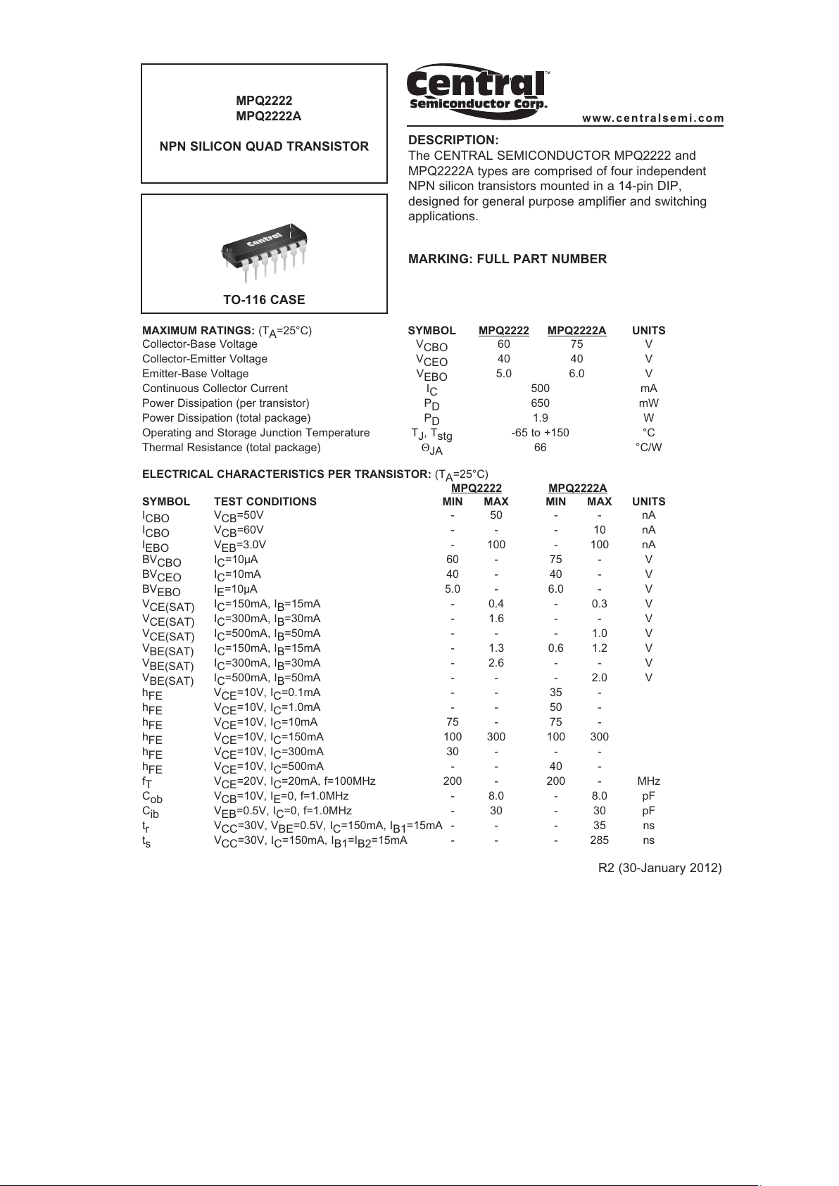
TO-116 CASE
R2 (30-January 2012)
www.centralsemi.com
Page 2
MPQ2222
MPQ2222A
NPN SILICON QUAD TRANSISTOR
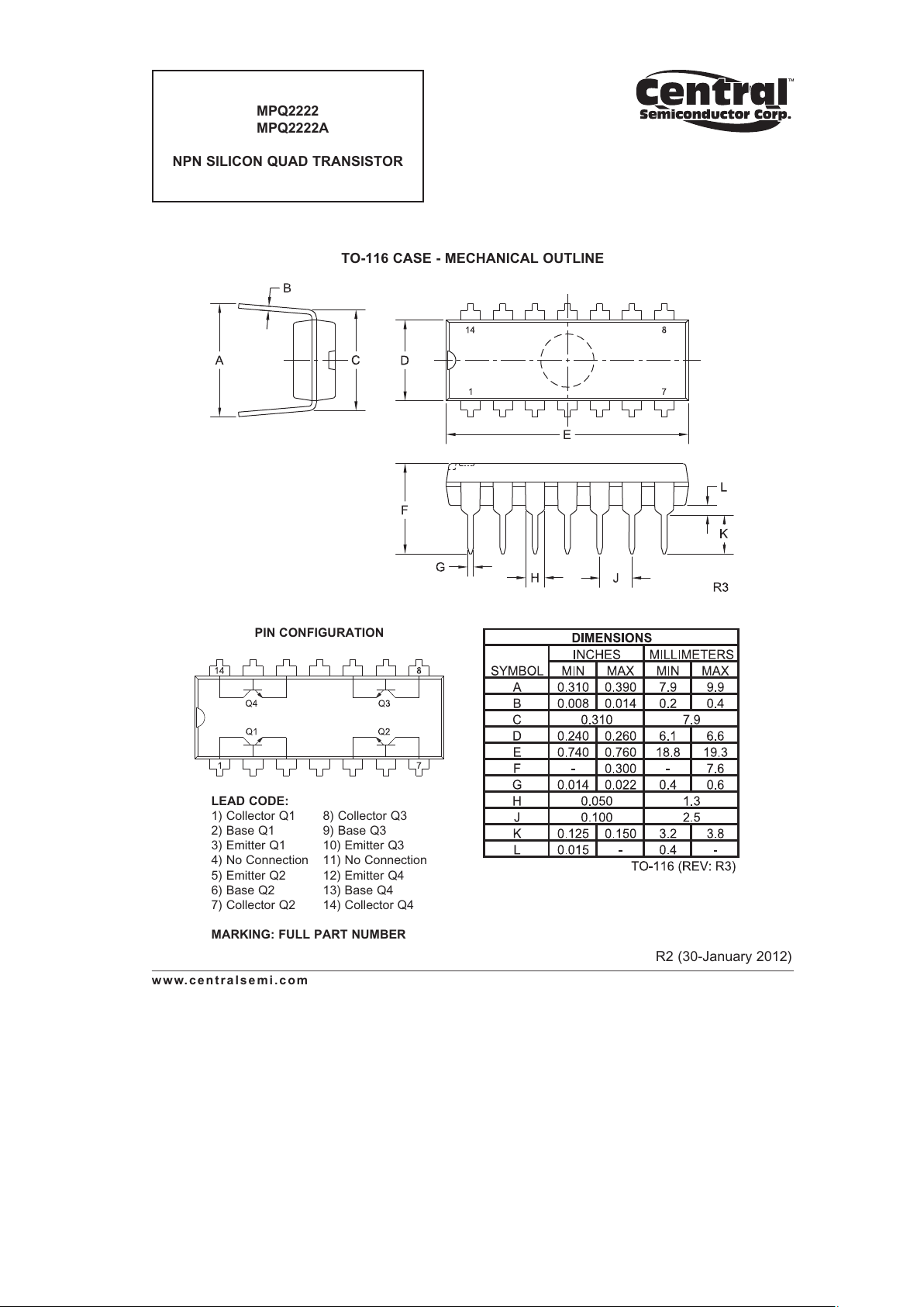
TO-116 CASE - MECHANICAL OUTLINE
LEAD CODE:
1) Collector Q1 8) Collector Q3
2) Base Q1 9) Base Q3
3) Emitter Q1 10) Emitter Q3
4) No Connection 11) No Connection
5) Emitter Q2 12) Emitter Q4
6) Base Q2 13) Base Q4
7) Collector Q2 14) Collector Q4
MARKING: FULL PART NUMBER
PIN CONFIGURATION
www.centralsemi.com
R2 (30-January 2012)
Page 3

For the latest version of Central Semiconductor’s LIMITATIONS AND DAMAGES DISCLAIMER,
which is part of Central’s Standard Terms and Conditions of sale, visit: www.centralsemi.com/terms
OUTSTANDING SUPPORT AND SUPERIOR SERVICES
PRODUCT SUPPORT
Central’s operations team provides the highest level of support to insure product is delivered on-time.
• Supply management (Customer portals) • Custom bar coding for shipments
• Inventory bonding • Custom product packing
• Consolidated shipping options
CONTACT US
Corporate Headquarters & Customer Support Team
Central Semiconductor Corp.
145 Adams Avenue
Hauppauge, NY 11788 USA
Main Tel: (631) 435-1110
Main Fax: (631) 435-1824
Support Team Fax: (631) 435-3388
www.centralsemi.com
Worldwide Field Representatives:
www.centralsemi.com/wwreps
Worldwide Distributors:
www.centralsemi.com/wwdistributors
DESIGNER SUPPORT/SERVICES
Central’s applications engineering team is ready to discuss your design challenges. Just ask.
• Free quick ship samples (2
nd
day air) • Special wafer diffusions
• Online technical data and parametric search • PbSn plating options
• SPICE models • Package details
• Custom electrical curves • Application notes
• Environmental regulation compliance • Application and design sample kits
• Customer specific screening • Custom product and package development
• Up-screening capabilities
www.centralsemi.com
Page 4

 Loading...