

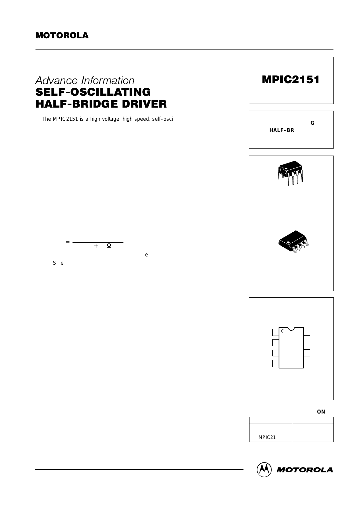
Page 1
1
Motorola Power Products Division Advanced Data
Power Products Division
The MPIC2151 is a high voltage, high speed, self–oscillating power MOSFET
and IGBT driver with both high side and low side referenced output channels. Proprietary HVIC and latch immune CMOS technologies enable ruggedized monolithic construction. The front–end features a programmable oscillator which is similar
to the 555 timer. The output drivers feature a high pulse current buf fer stage and an
internal deadtime designed for minimum driver cross–conduction. Propagation delays for the two channels are matched to simplify use in 50% duty cycle applications. The floating channel can be used to drive an N–channel power MOSFET or
IGBT in the high side configuration that operates off a high voltage rail from 10 to
600 volts.
• Floating Channel Designed for Bootstrap Operation
• Fully Operational to +600 V
• Tolerant to Negative Transient Voltage
• dV/dt Immune
• Undervoltage Lockout
• Programmable Oscillator Frequency:
f
+
1
1.4 (RT)75W) CT
• Matched Propagation Delay for Both Channels
• Low Side Output In Phase with RT
PRODUCT SUMMARY
V
OFFSET 600 V MAX
Duty Cycle
50%
V
OUT 10 – 20 V
t
r/f
(typical) 120 & 60 ns
Deadtime (typical) 1.2 µs
This document contains information on a new product. Specifications and information herein are subject
to change without notice.
REV 1
Order this document
by MPIC2151/D
SEMICONDUCTOR TECHNICAL DATA
Device
Package
SELF–OSCILLATING
HALF–BRIDGE
DRIVER
ORDERING INFORMATION
MPIC2151P PDIP
D SUFFIX
PLASTIC PACKAGE
CASE 751–05
(SO–8)
8
1
(TOP VIEW)
PIN CONNECTIONS
P SUFFIX
PLASTIC PACKAGE
CASE 626–05
8
1
MPIC2151D SOIC
V
B
8V
CC
RT
CT
COM
HO
V
S
LO
7
6
5
1
2
3
4
Motorola, Inc. 1996
Page 2
MPIC2151
2
Motorola Power Products Division Advanced Data
SIMPLIFIED BLOCK DIAGRAM
PULSE
GEN
PULSE
FILTER
HV
LEVEL
SHIFT
COM
LO
V
CC
V
S
V
B
HO
R
S
Q
DELAY
DEAD
TIME
DEAD
TIME
UV
DETECT
+
–
+
–
R
R
R
RT
CT
R
SQQ
15.6 V
ABSOLUTE MAXIMUM RATINGS
Absolute Maximum Ratings indicate sustained limits beyond which damage to the device may occur. All voltage parameters are absolute
voltages referenced to COM, all currents are defined positive into any lead. The Thermal Resistance and Power Dissipation ratings are
measured under board mounted and still air conditions.
Rating
Symbol Min Max Unit
High Side Floating Supply Absolute Voltage
V
–0.3
625
V
High Side Floating Supply Absolute Voltage
High Side Floating Supply Offset Voltage
V
B
V
–0.3
V
–25
625
V
+0.3
V
DC
High Side Floating Supply Offset Voltage
High Side Floating Output Voltage
V
S
V
HO
VB–25
VS–0.3
VB+0.3
VB+0.3
High Side Floating Output Voltage
Low Side Output Voltage
V
HO
V
LO
VS–0.3
–0.3
VB+0.3
VCC+0.3
Low Side Output Voltage
RT Voltage
V
LO
V
RT
–0.3
–0.3
VCC+0.3
VCC+0.3
CT Voltage
RT
V
CT
–0.3
CC
+0.3
VCC+0.3
Supply Current (Note 1) I
– 25 mA
Supply Current (Note 1)
High Side Output Current
I
CC
I
HO
–
–50025500
mA
DC
Low Side Output Current
HO
I
LO
–500
500
RT Output Current
IRT–5.0
5.0
Allowable Offset Supply Voltage Transient dVS/dt – 50 V/ns
*Package Power Dissipation @ TC ≤ +25°C (8 Lead DIP)
(8 Lead SOIC)
P
D
–
–
–
1.0
0.625
Watt
Operating and Storage Temperature Tj, T
stg
–55 150 °C
Thermal Resistance, Junction to Ambient (8 Lead DIP)
(8 Lead SOIC)
R
θJA
–
–
125
200
°C/W
Lead Temperature for Soldering Purposes, 10 seconds T
L
– 260 °C
RECOMMENDED OPERATING CONDITIONS
The Input/Output logic timing Diagram is shown in Figure 1. For proper operation the device should be used within the recommended conditions.
High Side Floating Supply Absolute Voltage
V
B
VS+10 VS+V
clamp
V
High Side Floating Supply Offset Voltage V
S
– 600
High Side Floating Output Voltage V
HO
V
S
V
B
Low Side Output Voltage V
LO
0 V
CC
Supply Current (Note 1) I
CC
– 5.0 mA
Ambient Temperature T
A
–40 125 °C
Note 1: Because the MPIC2151 is designed specifically for off–line supply systems, this IC contains a zener clamp structure between the chip
VCC and COM which has a nominal breakdown voltage of 15.6 V . Therefore, the IC supply voltage is normally derived by forcing current into
the supply lead (typically by means of a high value resistor connected between the chip VCC and the rectified line voltage and a local decoupling capacitor from VCC to COM) and allowing the internal zener clamp circuit to determine the nominal supply voltage. Therefore, this circuit
should not be driven by a DC, low impedance power source of greater than V
CLAMP
.
Page 3

MPIC2151
3
Motorola Power Products Division Advanced Data
ELECTRICAL CHARACTERISTICS (T
C
= 25°C unless otherwise specified)
Characteristic
Symbol Min Typ Max Unit
STATIC ELECTRICAL CHARACTERISTICS
Supply Characteristics
V
BIAS
(VCC, VBS) = 12 V, VSS = COM and CL = 1000 pF unless otherwise specified.
VCC Supply Undervoltage Positive Going Threshold
V
CCUV+
– 8.4 –
V
DC
VCC Supply Undervoltage Negative Going Threshold V
CCUV–
– 8.0 –
Quiescent VCC Supply Current I
QCC
– 400 – µA
VCC Zener Shunt Clamp Voltage @ IOC = 5 mA V
CLAMP
– 15.6 – V
DC
Floating Supply Characteristics
Offset Supply Leakage Current @ VB = VS = 600 V I
LK
– – 50
µA
DC
Quiescent VBS Supply Current I
QBS
– 10 –
Oscillator I/O Characteristics
Oscillator Frequency @ RT = 35.7 KΩ, CT = 1 nF f
OSC
– 20 –
kHz
Oscillator Frequency @ RT = 7.04 KΩ, CT = 1 nF f
OSC
– 100 –
CT Input Current I
CT
– 0.001 1.0 µA
CT Undervoltage Lockout @ 2.5 V < VCC < V
CCUV+
V
CTUV
– 0 –
mV
RT High Level Output Voltage, VCC – RT @ IRT = –100 µA
@ IRT = –1 mA
V
RT+
V
RT+
–
–
20
200
–
–
RT Low Level Output Voltage, VCC + RT @ IRT = 100 µA
@ IRT = 1 mA
V
RT–
V
RT–
–
–
20
200
–
–
RT Undervoltage Lockout, VCC – RT @ 2.5 V < VCC < V
CCUV+
V
RTUV
– 0 –
2/3 VCC Threshold V
CT+
– 8.0 –
V
DC
1/3 VCC Threshold V
CT–
– 4.0 –
Output Characteristics
High Level Output Voltage, V
BIAS–VO
@ IO = 0 A V
OH
– – 100
mV
Low Level Output Voltage, VO @ IO = 0 A V
OL
– – 100
Dynamic Electrical Characteristics
V
BIAS
(VCC, VBS) = 12 V and CL = 1000 pF unless otherwise specified. TA = 25°C.
Turn–On Rise Time t
r
– 120 –
ns
Turn–Off Fall Time t
f
– 60 –
Deadtime, LS Turn–Off to HS Turn–On & HS Turn–Off to LS Turn–On DT – 1.2 – µA
RT Duty Cycle, f
OSC
= 20 kHz DC – 50 – %
Page 4

MPIC2151
4
Motorola Power Products Division Advanced Data
TYPICAL CONNECTION
TO
LOAD
10 TO 600 V
V
CC
RT
COM
V
B
CT
HO
V
S
LO
LEAD DEFINITIONS
Symbol Lead Description
RT Oscillator timing resistor input; a resistor is connected from RT to CT. RT is in phase with LO for normal IC operation.
CT Oscillator timing capacitor input; a capacitor is connected from CT to COM in order to program the oscillator frequency
according to the following equation:
where 75Ω is the effective impedance of the RT output stage.
V
B
High Side Floating Supply
HO High Side Gate Drive Output
V
S
High Side Floating Supply Return
V
CC
Logic and Low Side Fixed Supply
LO Low Side Gate Drive Output
COM Logic and Low Side Return
Figure 1. Input / Output Timing Diagram
Figure 2. Switching Time Waveform Definitions
Figure 3. Deadtime Waveform Definitions
LO
HO
V
CLAMP
V
CCUV+
V
CC
RT
CT
RT(HO)
RT(LO)
LO
HO
50% 50%
10% 10%
90% 90%
t
r
t
f
50%50%
RT
HO
LO
90%
90%
10%
10%
DT
f
+
1
1.4 (RT)75W) CT
Page 5

MPIC2151
5
Motorola Power Products Division Advanced Data
PACKAGE DIMENSIONS
CASE 626–05
ISSUE K
NOTES:
1. DIMENSION L TO CENTER OF LEAD WHEN
FORMED PARALLEL.
2. PACKAGE CONTOUR OPTIONAL (ROUND OR
SQUARE CORNERS).
3. DIMENSIONING AND TOLERANCING PER ANSI
Y14.5M, 1982.
STYLE 1:
PIN 1. AC IN
2. DC + IN
3. DC – IN
4. AC IN
5. GROUND
6. OUTPUT
7. AUXILIARY
8. V
CC
1 4
58
F
NOTE 2
–A–
–B–
–T–
SEATING
PLANE
H
J
G
D
K
N
C
L
M
M
A
M
0.13 (0.005) B
M
T
DIM MIN MAX MIN MAX
INCHESMILLIMETERS
A 9.40 10.16 0.370 0.400
B 6.10 6.60 0.240 0.260
C 3.94 4.45 0.155 0.175
D 0.38 0.51 0.015 0.020
F 1.02 1.78 0.040 0.070
G 2.54 BSC 0.100 BSC
H 0.76 1.27 0.030 0.050
J 0.20 0.30 0.008 0.012
K 2.92 3.43 0.115 0.135
L 7.62 BSC 0.300 BSC
M ––– 10 ––– 10
N 0.76 1.01 0.030 0.040
_ _
CASE 751–05
ISSUE P
SEATING
PLANE
1
4
58
C
K
4X P
A0.25 (0.010)MT B
S S
0.25 (0.010)
M
B
M
8X D
R
M
J
X 45
_
_
F
–A–
–B–
–T–
DIM MIN MAX
MILLIMETERS
A 4.80 5.00
B 3.80 4.00
C 1.35 1.75
D 0.35 0.49
F 0.40 1.25
G 1.27 BSC
J 0.18 0.25
K 0.10 0.25
M 0 7
P 5.80 6.20
R 0.25 0.50
__
G
NOTES:
1. DIMENSIONS A AND B ARE DATUMS AND T IS A
DATUM SURFACE.
2. DIMENSIONING AND TOLERANCING PER ANSI
Y14.5M, 1982.
3. DIMENSIONS ARE IN MILLIMETER.
4. DIMENSION A AND B DO NOT INCLUDE MOLD
PROTRUSION.
5. MAXIMUM MOLD PROTRUSION 0.15 PER SIDE.
6. DIMENSION D DOES NOT INCLUDE MOLD
PROTRUSION. ALLOWABLE DAMBAR
PROTRUSION SHALL BE 0.127 TOTAL IN EXCESS
OF THE D DIMENSION AT MAXIMUM MATERIAL
CONDITION.
Page 6

MPIC2151
6
Motorola Power Products Division Advanced Data
Motorola reserves the right to make changes without further notice to any products herein. Motorola makes no warranty , representation or guarantee regarding
the suitability of its products for any particular purpose, nor does Motorola assume any liability arising out of the application or use of any product or circuit, and
specifically disclaims any and all liability, including without limitation consequential or incidental damages. “T ypical” parameters which may be provided in Motorola
data sheets and/or specifications can and do vary in different applications and actual performance may vary over time. All operating parameters, including “Typicals”
must be validated for each customer application by customer’s technical experts. Motorola does not convey any license under its patent rights nor the rights of
others. Motorola products are not designed, intended, or authorized for use as components in systems intended for surgical implant into the body, or other
applications intended to support or sustain life, or for any other application in which the failure of the Motorola product could create a situation where personal injury
or death may occur. Should Buyer purchase or use Motorola products for any such unintended or unauthorized application, Buyer shall indemnify and hold Motorola
and its officers, employees, subsidiaries, affiliates, and distributors harmless against all claims, costs, damages, and expenses, and reasonable attorney fees
arising out of, directly or indirectly, any claim of personal injury or death associated with such unintended or unauthorized use, even if such claim alleges that
Motorola was negligent regarding the design or manufacture of the part. Motorola and are registered trademarks of Motorola, Inc. Motorola, Inc. is an Equal
Opportunity/Affirmative Action Employer.
How to reach us:
USA/EUROPE/Locations Not Listed: Motorola Literature Distribution; JAPAN: Nippon Motorola Ltd.; Tatsumi–SPD–JLDC, 6F Seibu–Butsuryu–Center,
P.O. Box 20912; Phoenix, Arizona 85036. 1–800–441–2447 or 602–303–5454 3–14–2 Tatsumi Koto–Ku, Tokyo 135, Japan. 03–81–3521–8315
MFAX: RMFAX0@email.sps.mot.com – TOUCHTONE 602–244–6609 ASIA/PACIFIC: Motorola Semiconductors H.K. Ltd.; 8B Tai Ping Industrial Park,
INTERNET: http://Design–NET.com 51 Ting Kok Road, Tai Po, N.T., Hong Kong. 852–26629298
MPIC2151/D
*MPIC2151/D*
◊
 Loading...