

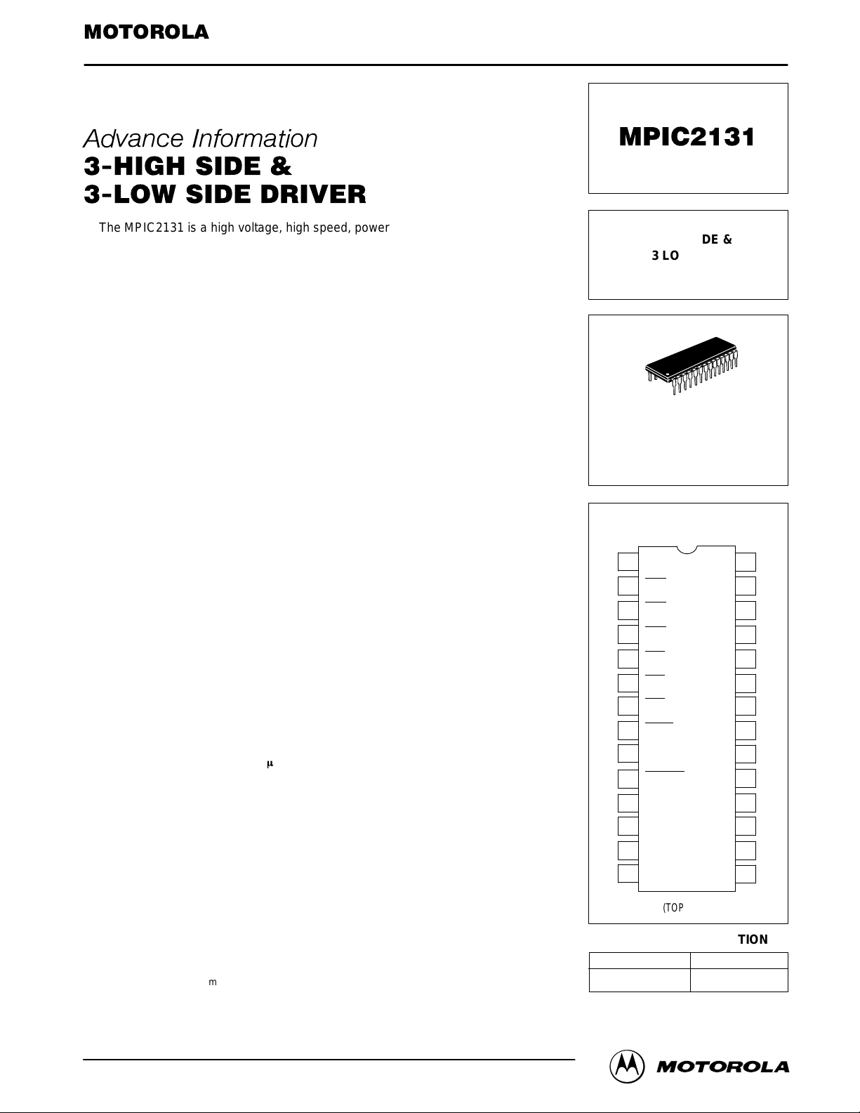
Page 1
1
Motorola Power Products Division Advanced Data
Power Products Division
The MPIC2131 is a high voltage, high speed, power MOSFET and IGBT driver
with three independent high side and low side referenced output channels for
3–Phase applications. Proprietary HVIC technology enables ruggedized monolithic construction. Logic inputs are compatible with 5 V CMOS or LSTTL outputs. A
ground referenced operational amplifier provides an analog feedback of bridge
current via an external current sense resistor. A current trip function which terminates all six outputs is also derived from an external current sense resistor. An extra shutdown input is provided for customizing the shutdown function. An open
drain FAULT signal is provided to indicate that any of shutdown conditions has occurred. The output drivers feature a high pulse current buffer stage designed for
minimum driver cross–conduction. Propagation delays are matched to simplify use
in high frequency applications.
The floating channels can be used to drive N–channel power MOSFET or
IGBT’s in the high side configuration which operate from 10 to 600 volts.
• Floating Channel Designed for Bootstrap Operation
• Fully Operational to +600 V
• Tolerant to Negative Transient Voltage
• dV/dt Immune
• Gate Drive Supply Range from 10 to 20 V
• Undervoltage Lockout for All Channels
• Over–current Shut Down Turns Off All Six Drivers
• Independent 3 High Side & 3 Low Side Drivers
• Matched Propagation Delay for All Channels
• Outputs Out of Phase with Inputs
PRODUCT SUMMARY
V
OFFSET 600 V MAX
I
O+/– 200 mA/420 mA
V
OUT 10 – 20 V
t
on/off
(typical)
1.4 & 0.7 m
s
Delay Matching
700 ns
This document contains information on a new product. Specifications and information herein are subject
to change without notice.
REV 1
Order this document
by MPIC2131/D
SEMICONDUCTOR TECHNICAL DATA
Device
Package
3 HIGH SIDE &
3 LOW SIDE
DRIVER
ORDERING INFORMATION
(TOP VIEW)
PIN CONNECTIONS
P SUFFIX
PLASTIC PACKAGE
CASE 710–02
MPIC2131P PDIP
28
1
1
2
3
4
5
6
7
8
22
23
24
25
26
27
28
9
21
20
10
11
12
13
14
17
18
19
16
15
V
CC
HIN1
HIN2
HIN3
LIN1
LIN2
LIN3
FAULT
ITRIP
FLT+CLR
SD
V
SS
COM
LO3
V
B1
HO1
V
S1
V
B2
HO2
V
S2
V
B3
HO3
V
S3
LO1
LO2
Motorola, Inc. 1996
Page 2
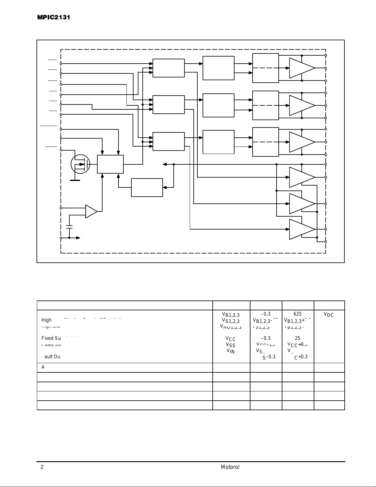
MPIC2131
2
Motorola Power Products Division Advanced Data
SIMPLIFIED BLOCK DIAGRAM
LATCH
UV
DETECTOR
DRIVER
PULSE
GENERATOR
LEVEL
SHIFTER
SET
RESET
LATCH
UV
DETECTOR
DRIVER
PULSE
GENERATOR
LEVEL
SHIFTER
SET
RESET
LATCH
UV
DETECTOR
DRIVER
SET
RESET
DRIVER
DRIVER
DRIVER
PULSE
GENERATOR
LEVEL
SHIFTER
INPUT
SIGNAL
GENERATOR
INPUT
SIGNAL
GENERATOR
INPUT
SIGNAL
GENERATOR
UNDER–
VOLTAGE
DETECTOR
FAULT
LOGIC
V
CC
V
B3
V
S2
V
S1
V
B1
HO1
H1
L1
H2
L2
H3
L3
CURRENT
COMPARATOR
V
B2
HO2
V
S3
LO1
LO2
LO3
COM
HIN1
HIN2
HIN3
LIN1
LIN2
LIN3
FLT–CLR
V
SS
ITRIP
HO3
0.5 V
SD
FAULT
V
SS
ABSOLUTE MAXIMUM RATINGS
Absolute Maximum Ratings indicate sustained limits beyond which damage to the device may occur. All voltage parameters are absolute
voltages referenced to COM. The Thermal Resistance and Power Dissipation ratings are measured under board mounted and still air
conditions.
Rating
Symbol Min Max Unit
High Side Floating Supply Offset Voltage
B1,2,3
V
S1,2,3
V
B1,2,3
–25
V
B1,2,3
+0.3
DC
High Side Floating Output Voltage
Low Side Output Voltage
V
HO1,2,3
V
LO1,2,3
V
S1,2,3
–0.3
–0.3
V
B1,2,3
+0.3
VCC+0.3
LO1,2,3
V
CC
CC
+0.3
25
Fixed Supply Offset Voltage
Logic Input Voltage (HIN–, LIN–, FLT–, CLR–, SD & ITRIP)
V
SS
V
IN
VCC–25
VSS–0.3
VCC+0.3
VCC+0.3
IN
FAULT
SS
–0.3
VSS–0.3
CC
+0.3
VCC+0.3
Allowable Offset Supply Voltage Transient dVS/dt – 50 V/ns
*Package Power Dissipation @ TC ≤ +25°C (28 Lead DIP) P
D
– 1.5 Watt
Operating and Storage Temperature Tj, T
stg
–55 150 °C
Thermal Resistance, Junction to Ambient (8 Lead DIP) R
θJA
– 83 °C/W
Lead Temperature for Soldering Purposes, 10 seconds T
L
– 260 °C
High Side Floating Absolute Voltage
Fixed Supply Voltage
Fault Output Voltage
V
B1,2,3
–0.3
–0.3
625
V
DC
Page 3

MPIC2131
3
Motorola Power Products Division Advanced Data
RECOMMENDED OPERATING CONDITIONS
The Input/Output logic timing Diagram is shown in Figure 1. For proper operation the device should be used within the recommended conditions. The VS offset rating is tested with all supplies biased at 15 V differential.
High Side Floating Supply Absolute Voltage
V
B1,2,3
V
S1,2,3
+10 V
S1,2,3
+20 V
High Side Floating Supply Offset Voltage V
S1,2,3
Note 1 VSO+600 V
High Side Floating Output Voltage V
HO1,2,3
V
S1,2,3
V
B1,2,3
V
Fixed Supply Voltage V
CC
10 20 V
Low Side Output Voltage V
LO1,2,3
0 V
CC
V
Low Side Driver Return V
SS
–5 5 V
Logic Input Voltage (HIN–, LIN–, FLT–CLR, SD & ITRIP) V
IN
V
SS
5 V
Fault Output Voltage FAULT– V
SS
V
CC
V
Ambient Temperature T
A
–40 125 °C
Note 1: Logic operational for VS of –5 V to +600 V. Logic state held for VS of –5 V to –VBS.
ELECTRICAL CHARACTERISTICS (T
A
= 25°C unless otherwise specified)
Characteristic
Symbol Min Typ Max Unit
STATIC ELECTRICAL CHARACTERISTICS
V
BIAS
(VCC, V
BS1,2,3
) = 15 V and VSS = COM unless otherwise specified. The VIN, VTH and IIN parameters are referenced to VSS and are
applicable to all six channels (HS1,2,3 & LS1,2,3). The VO and IO parameters are referenced to COM and V
SO1,2,3
and are applicable to
the respective output leads: HO1,2,3 or LO1,2,3.
Logic “0” Input Voltage (OUT = LO) V
IH
2.2 – – V
Logic “1” Input Voltage (OUT = HI) V
IL
– – 0.8 V
Logic “0” Fault Clear Input Voltage V
FCLR,IH
2.2 – – V
Logic “1” Fault Clear Input Voltage V
FCLR,IL
– – 0.8 V
SD Input Positive Going Threshold V
SD,TH+
– 1.8 – V
SD Input Negative Going Threshold V
SD,TH–
– 1.5 – V
ITRIP Input Positive Going Threshold V
IT,TH+
– 485 – mV
ITRIP Input Negative Going Threshold V
IT,TH–
– 400 – mV
High Level Output Voltage, V
BIAS–VO
@ VIN = 0 V, IO = 0 A V
OH
– – 100 mV
Low Level Output Voltage, VO @ VIN = 5 V, IO = 0 A V
OL
– – 100 mV
Offset Supply Leakage Current @ V
B1,2,3
= V
S1,2,3
= 600 V I
LK
– – 50 µA
Quiescent VBS Supply Current @ VIN = 0 V or 5 V I
QBS
– 30 – µA
Quiescent VCC Supply Current @ VIN = 0 V or 5 V I
QCC
– 3.0 – mA
Logic “1” Input Bias Current (OUT = HI) @ VIN = 0 V I
IN+
– 190 – µA
Logic “0” Input Bias Current (OUT = LO) @ VIN = 5 V I
IN–
– 100 – µA
“High” ITRIP Bias Current @ ITRIP = 5 V I
TRIP+
– 60 – µA
“Low” ITRIP Bias Current @ ITRIP = 0 V I
TRIP–
– – 50 nA
Logic “1” Fault Clear Bias Current @ FLT–CLR = 0 V I
FCLR+
– 190 – µA
Logic “0” Fault Clear Bias Current @ FLT–CLR = 5 V I
FCLR–
– 100 – µA
Logic “1” Shut Down Bias Current @ SD = 5 V I
SD+
– 60 – µA
Logic “0” Shut Down Bias Current @ SD = 5 V I
SD–
– – 150 nA
VBS Supply Undervoltage Positive Going Threshold V
BSUV+
– 8.6 – V
VBS Supply Undervoltage Negative Going Threshold V
BSUV–
– 8.2 – V
VCC Supply Undervoltage Positive Going Threshold V
CCUV+
– 9.0 – V
VCC Supply Undervoltage Negative Going Threshold V
CCUV–
– 8.7 – V
FAULT – Low On Resistance R
on,FLT
– 55 – Ω
Output High Short Circuit Pulsed Current @ V
out
= 0 V, Vin = 0 V, PW ≤ 10 µs I
O+
200 250 – mA
Output Low Short Circuit Pulsed Current @ V
out
= 15 V, Vin = 5 V, PW ≤ 10 µs I
O–
420 500 – mA
Page 4

MPIC2131
4
Motorola Power Products Division Advanced Data
ELECTRICAL CHARACTERISTICS
(T
A
= 25°C unless otherwise specified)
Characteristic
Symbol Min Typ Max Unit
DYNAMIC ELECTRICAL CHARACTERISTICS
V
BIAS
(VCC, V
BS1,2,3
) = 15 V, V
SO1,2,3
= VSS and CL = 1000 pF unless otherwise specified. TA = 25°C.
Turn–On Propagation Delay @ VIN = 0 & 5 V, V
S1,2,3
= 0 V to 600 V t
on
– 1.4 – µs
Turn–Off Propagation Delay @ VIN = 0 & 5 V, V
S1,2,3
= 0 V to 600 V t
off
– 0.7 – µs
Turn–On Rise Time @ VIN = 0 & 5 V, V
S1,2,3
= 0 V to 600 V t
r
– 80 – ns
Turn–On Fall Time @ VIN = 0 & 5 V, V
S1,2,3
= 0 V to 600 V t
f
– 40 – ns
ITRIP to Output Shutdown Propagation Delay @ VIN, V
ITRIP
= 0 & 5 V t
itrip
– 550 – ns
ITRIP Blanking Time @ ITRIP = 1 V t
bl
– 400 – ns
ITRIP to FAULT– Propagation Delay @ VIN, V
ITRIP
= 0 & 5 V t
flt
– 450 – ns
Input Filter Time (all six inputs) @ VIN = 0 & 5 V t
flt,in
– 310 – ns
FLT–CLR to FAULT Clear Time @ VIN, VIT, VFC = 0 & 5 V t
fltclr
– 450 – ns
SD to OUTPUT Shutdown Propagation Delay @ VIN, VSD = 0 & 5 V t
sd
– 550 – ns
Deadtime, LS Turn–Off to HS Turn–On & HS Turn–Off to LS Turn–On
@ VIN = 0 & 5 V
DT – 700 – ns
TYPICAL CONNECTION
10 TO 600 V
TO
LOAD
V
CC
ITRIP
COM
V
B1,2,3
HIN1,2,3
V
SS
SD
FLT–CLR
LIN1,2,3
FAULT
HO1,2,3
V
S1,2,3
LO1,2,3
LEAD DEFINITIONS
Symbol Lead Description
HIN1,2,3 Logic Inputs for High Side Gate Driver Outputs (HO1,2,3), Out of Phase
LIN1,2,3 Logic Inputs for Low Side Gate Driver Outputs (LO1,2,3), Out of Phase
FLT–CLR Logic Inputs for Fault Clear
SD Logic Input for Shut Down
FAULT Indicates Over–current, Shut Down or Low Side Undervoltage Condition, Negative Logic
ITRIP Input for Over–current Shut Down
V
SS
Logic Ground
V
B1,2,3
High Side Floating Supplies
HO1,2,3 High Side Gate Drive Outputs
V
S1,2,3
High Side Floating Supply Returns
V
CC
Logic and Low Side Fixed Supply
LO1,2,3 Low Side Gate Drive Outputs
COM Low Side Return
Page 5

MPIC2131
5
Motorola Power Products Division Advanced Data
Figure 1. Input / Output Timing Diagram
Figure 2. Switching Time Waveform
Definitions
Figure 3. Deadtime Waveform Definitions
LO
HO
HIN
LIN
50% 50%
50% 50%
DT DT
HIN
LIN
ITRIP
FAULT
HO
LO
HIN
LIN
LO
HO
50% 50%
10% 10%
90% 90%
t
on
t
r
t
off
t
f
50%
50%
50%
50%
50%
t
flt
LO2
FAULT
ITRIP
LIN2
t
itrip
t
fltclr
Figure 4. Shutdown Waveform Definitions
FLT–CLR
SD
SD
FLT–CLR
t
sd
50%
50%
Page 6

MPIC2131
6
Motorola Power Products Division Advanced Data
PACKAGE DIMENSIONS
CASE 710–02
ISSUE B
NOTES:
1. POSITIONAL TOLERANCE OF LEADS (D), SHALL
BE WITHIN 0.25 (0.010) AT MAXIMUM MATERIAL
CONDITION, IN RELATION TO SEATING PLANE
AND EACH OTHER.
2. DIMENSION L TO CENTER OF LEADS WHEN
FORMED PARALLEL.
3. DIMENSION B DOES NOT INCLUDE MOLD FLASH.
1
SEATING
PLANE
15
14
28
M
A
B
K
C
N
F
G
D
H
J
L
DIM MIN MAX MIN MAX
INCHESMILLIMETERS
A 36.45 37.21 1.435 1.465
B 13.72 14.22 0.540 0.560
C 3.94 5.08 0.155 0.200
D 0.36 0.56 0.014 0.022
F 1.02 1.52 0.040 0.060
G 2.54 BSC 0.100 BSC
H 1.65 2.16 0.065 0.085
J 0.20 0.38 0.008 0.015
K 2.92 3.43 0.115 0.135
L 15.24 BSC 0.600 BSC
M 0 15 0 15
N 0.51 1.02 0.020 0.040
_ __ _
Motorola reserves the right to make changes without further notice to any products herein. Motorola makes no warranty , representation or guarantee regarding
the suitability of its products for any particular purpose, nor does Motorola assume any liability arising out of the application or use of any product or circuit, and
specifically disclaims any and all liability , including without limitation consequential or incidental damages. “Typical” parameters which may be provided in Motorola
data sheets and/or specifications can and do vary in different applications and actual performance may vary over time. All operating parameters, including “Typicals”
must be validated for each customer application by customer’s technical experts. Motorola does not convey any license under its patent rights nor the rights of
others. Motorola products are not designed, intended, or authorized for use as components in systems intended for surgical implant into the body, or other
applications intended to support or sustain life, or for any other application in which the failure of the Motorola product could create a situation where personal injury
or death may occur. Should Buyer purchase or use Motorola products for any such unintended or unauthorized application, Buyer shall indemnify and hold Motorola
and its officers, employees, subsidiaries, affiliates, and distributors harmless against all claims, costs, damages, and expenses, and reasonable attorney fees
arising out of, directly or indirectly, any claim of personal injury or death associated with such unintended or unauthorized use, even if such claim alleges that
Motorola was negligent regarding the design or manufacture of the part. Motorola and are registered trademarks of Motorola, Inc. Motorola, Inc. is an Equal
Opportunity/Affirmative Action Employer.
How to reach us:
USA/EUROPE/Locations Not Listed: Motorola Literature Distribution; JAPAN: Nippon Motorola Ltd.; Tatsumi–SPD–JLDC, 6F Seibu–Butsuryu–Center,
P.O. Box 20912; Phoenix, Arizona 85036. 1–800–441–2447 or 602–303–5454 3–14–2 Tatsumi Koto–Ku, Tokyo 135, Japan. 03–81–3521–8315
MFAX: RMFAX0@email.sps.mot.com – TOUCHTONE 602–244–6609 ASIA/PACIFIC: Motorola Semiconductors H.K. Ltd.; 8B Tai Ping Industrial Park,
INTERNET: http://Design–NET.com 51 Ting Kok Road, Tai Po, N.T., Hong Kong. 852–26629298
MPIC2131/D
*MPIC2131/D*
◊
 Loading...