

Page 1

1
Motorola Small–Signal Transistors, FETs and Diodes Device Data
N–Channel — Depletion
MAXIMUM RATINGS
Rating Symbol Value Unit
Drain–Source Voltage V
DS
25 Vdc
Drain–Gate Voltage V
DG
25 Vdc
Gate–Source Voltage V
GS
–25 Vdc
Gate Current I
G
10 mAdc
Total Device Dissipation @ TA = 25°C
Derate above 25°C
P
D
350
2.8
mW
mW/°C
Junction Temperature Range T
J
125 °C
Storage Temperature Range T
stg
–65 to +150 °C
ELECTRICAL CHARACTERISTICS (T
A
= 25°C unless otherwise noted)
Characteristic Symbol Min Max Unit
OFF CHARACTERISTICS
Gate–Source Breakdown Voltage
(IG = –10 µAdc, VDS = 0)
V
(BR)GSS
–25 — Vdc
Gate Reverse Current
(VGS = –15 Vdc, VDS = 0)
(VGS = –15 Vdc, VDS = 0, TA = 100°C)
I
GSS
—
—
–2.0
–2.0
nAdc
µAdc
Gate–Source Cutoff Voltage
(VDS = 15 Vdc, ID = 2.0 nAdc)
V
GS(off)
— –8.0 Vdc
Gate–Source Voltage
(VDS = 15 Vdc, ID = 0.2 mAdc)
V
GS
–0.5 –7.5 Vdc
ON CHARACTERISTICS
Zero–Gate–Voltage Drain Current
(1)
(VDS = 15 Vdc, VGS = 0 Vdc)
I
DSS
2.0 20 mAdc
SMALL–SIGNAL CHARACTERISTICS
Forward Transfer Admittance
(1)
(VDS = 15 Vdc, VGS = 0, f = 1.0 kHz)
(VDS = 15 Vdc, VGS = 0, f = 100 MHz)
yfs
2000
1600
7500
—
m
mhos
Input Admittance
(VDS = 15 Vdc, VGS = 0, f = 100 MHz)
Re(yis) — 800
m
mhos
Output Conductance
(VDS = 15 Vdc, VGS = 0, f = 100 MHz)
Re(yos) — 200
m
mhos
Input Capacitance
(VDS = 15 Vdc, VGS = 0, f = 1.0 MHz)
C
iss
— 7.0 pF
Reverse Transfer Capacitance
(VDS = 15 Vdc, VGS = 0, f = 1.0 MHz)
C
rss
— 3.0 pF
1. Pulse Test; Pulse Width v 630 ms, Duty Cycle v 10%.
Order this document
by MPF102/D
SEMICONDUCTOR TECHNICAL DATA
CASE 29–04, STYLE 5
TO–92 (TO–226AA)
1
2
3
Motorola, Inc. 1997
1 DRAIN
2 SOURCE
3
GATE
Page 2

MPF102
2
Motorola Small–Signal Transistors, FETs and Diodes Device Data
P
G
, POWER GAIN (dB)
POWER GAIN
2.0
ID, DRAIN CURRENT (mA)
Figure 1. Effects of Drain Current
4.0
24
8.0
12
16
20
0 4.0 6.0 8.0 10 12 14
f = 100 MHz
400 MHz
T
channel
= 25°C
VDS = 15 Vdc
VGS = 0 V
Figure 2. 100 MHz and 400 MHz Neutralized Test Circuit
*L1 17 turns, (approx. — depends upon circuit layout) AWG #28
enameled copper wire, close wound on 9/32″ ceramic coil
form. Tuning provided by a powdered iron slug.
*L2 4–1/2 turns, AWG #18 enameled copper wire, 5/16″ long,
3/8″ I.D. (AIR CORE).
*L3 3–1/2 turns, AWG #18 enameled copper wire, 1/4″ long,
3/8″ I.D. (AIR CORE).
**L1 6 turns, (approx. — depends upon circuit layout) AWG #24
enameled copper wire, close wound on 7/32″ ceramic coil
form. Tuning provided by an aluminum slug.
**L2 1 turn, AWG #16 enameled copper wire, 3/8″ I.D.
(AIR CORE).
**L3 1/2 turn, AWG #16 enameled copper wire, 1/4″ I.D.
(AIR CORE).
Adjust VGS for
ID = 50 mA
VGS < 0 Volts
NOTE: The noise source is a hot–cold body
(AIL type 70 or equivalent) with a
test receiver (AIL type 136 or equivalent).
Reference
Designation
VALUE
100 MHz 400 MHz
C1
7.0 pF 1.8 pF
C2 1000 pF 17 pF
C3 3.0 pF 1.0 pF
C4 1–12 pF 0.8–8.0 pF
C5 1–12 pF 0.8–8.0 pF
C6 0.0015 µF 0.001 µF
C7 0.0015 µF 0.001 µF
L1 3.0 µH* 0.2 µH**
L2 0.15 µH* 0.03 µH**
L3 0.14 µH* 0.022 µH**
INPUT
TO 50
Ω
SOURCE
NEUTRALIZING
COIL
L1
C5
L3R
g
′
C1
C6
C4
L2
C3
TO 500
Ω
LOAD
CASE
C7
COMMON
ID = 5.0 mA
V
GS
V
DS
+15 V
C2
Page 3
MPF102
3
Motorola Small–Signal Transistors, FETs and Diodes Device Data
NF, NOISE FIGURE (dB)
2.0
VDS, DRAIN–SOURCE VOLTAGE (VOLTS)
0
10
2.0
4.0
6.0
8.0
0 4.0 6.0 8.0 10 12 14
ID = 5.0 mA
100 MHz
VDS = 15 Vdc
f1 = 399 MHz
f2 = 400 MHz
NF, NOISE FIGURE (dB)
2.0
ID, DRAIN CURRENT (mA)
1.5
6.5
2.5
3.5
4.5
5.5
0 4.0 6.0 8.0 10 12 14
Figure 3. Effects of Drain–Source Voltage Figure 4. Effects of Drain Current
NOISE FIGURE
(T
channel
= 25°C)
Pin, INPUT POWER PER TONE (dB)
+40
Figure 5. Third Order Intermodulation Distortion
P , OUTPUT POWER PER TONE (dB)
out
16 18 20
f = 400 MHz
f = 400 MHz
100 MHz
VDS = 15 V
VGS = 0 V
+20
0
–20
–40
–60
–80
–100
–120
–140
–160
–120 –100 –80 –60 –40 –20 0 +20
3RD ORDER INTERCEPT
FUNDAMENT AL
OUTPUT @ I
DSS
,
0.25 I
DSS
3RD ORDER IMD
OUTPUT @ I
DSS
,
0.25 I
DSS
INTERMODULA TION CHARACTERISTICS
Page 4

MPF102
4
Motorola Small–Signal Transistors, FETs and Diodes Device Data
f, FREQUENCY (MHz)
30
10
bis @ I
DSS
f, FREQUENCY (MHz)
5.0
Figure 6. Input Admittance (yis) Figure 7. Reverse Transfer Admittance (yrs)
COMMON SOURCE CHARACTERISTICS
ADMITTANCE PARAMETERS
(VDS = 15 Vdc, T
channel
= 25°C)
f, FREQUENCY (MHz)
20
f, FREQUENCY (MHz)
10
Figure 8. Forward Transadmittance (yfs) Figure 9. Output Admittance (yos)
g
is
, INPUT CONDUCT ANCE (mmhos)
20
10
0.3
0.5
0.7
1.0
2.0
3.0
5.0
7.0
20 30 50 70 100 200 300
500 700
1000
b
is
, INPUT SUSCEPT ANCE (mmhos)
g
fs
, FORWARD TRANSCONDUCTANCE (mmhos)
|b
fs
|, FORWARD SUSCEPTANCE (mmhos)
g
rs
, REVERSE TRANSADMITTANCE (mmhos)
b
rs
, REVERSE SUSCEPTANCE (mmhos)
0.2
0.3
0.5
0.7
1.0
2.0
3.0
5.0
7.0
10
g
os
, OUTPUT ADMITTANCE (mhos)
b
os
, OUTPUT SUSCEPT ANCE (mhos)
3.0
0.05
0.07
0.1
0.2
0.3
0.7
0.5
1.0
2.0
10 20 30 50 70 100 200 300
500 700
1000
10 20 30 50 70 100 200 300
500 700
1000
0.01
0.02
0.05
0.1
0.2
0.5
1.0
2.0
5.0
10 20 30 50 70 100 200 300
500 700
1000
bis @ 0.25 I
DSS
gis @ I
DSS
gis @ 0.25 I
DSS
brs @ I
DSS
0.25 I
DSS
grs @ I
DSS
, 0.25 I
DSS
gfs @ I
DSS
|bfs| @ I
DSS
|bfs| @ 0.25 I
DSS
bos @ I
DSS
and 0.25 I
DSS
gos @ I
DSS
gos @ 0.25 I
DSS
gfs @ 0.25 I
DSS
Page 5

MPF102
5
Motorola Small–Signal Transistors, FETs and Diodes Device Data
Figure 10. S
11s
Figure 11. S
12s
0°350°340°330
°
10
°
20
°
30
°
180°190°200°210
°
170
°
160
°
150
°
320
°
310
°
300
°
290
°
280
°
270
°
260
°
250
°
240
°
230
°
220
°
40
°
50
°
60
°
70
°
80
°
90
°
100
°
110
°
120
°
130
°
140
°
0°350°340°330
°
10
°
20
°
30
°
180°190°200°210
°
170
°
160
°
150
°
320
°
310
°
300
°
290
°
280
°
270
°
260
°
250
°
240
°
230
°
220
°
40
°
50
°
60
°
70
°
80
°
90
°
100
°
110
°
120
°
130
°
140
°
0°350°340°330
°
10
°
20
°
30
°
180°190°200°210
°
170
°
160
°
150
°
320
°
310
°
300
°
290
°
280
°
270
°
260
°
250
°
240
°
230
°
220
°
40
°
50
°
60
°
70
°
80
°
90
°
100
°
110
°
120
°
130
°
140
°
0°350°340°330
°
10
°
20
°
30
°
180°190°200°210
°
170
°
160
°
150
°
320
°
310
°
300
°
290
°
280
°
270
°
260
°
250
°
240
°
230
°
220
°
40
°
50
°
60
°
70
°
80
°
90
°
100
°
110
°
120
°
130
°
140
°
1.0
0.9
0.8
0.7
0.6
0.4
0.3
0.2
0.1
0.0
1.0
0.9
0.8
0.7
0.6
0.6
0.5
0.4
0.3
0.3
0.4
0.5
0.6
900
900
800
700
600
500
400
300
200
100
800
700
600
500
400
300
200
100
ID = 0.25 I
DSS
ID = I
DSS
100
200
300
400
600
700
800
900
500
ID = I
DSS
, 0.25 I
DSS
900
500
800
700
600
500
400
300
200
100
ID = 0.25 I
DSS
ID = I
DSS
100
200
300
400
900
600
700
800
900
800
600
400
300
200
200
100
ID = 0.25 I
DSS
ID = I
DSS
900
100
500
700
300
400
500
600
700
800
Figure 12. S
21s
Figure 13. S
22s
COMMON SOURCE CHARACTERISTICS
S–PARAMETERS
(VDS = 15 Vdc, T
channel
= 25°C, Data Points in MHz)
Page 6

MPF102
6
Motorola Small–Signal Transistors, FETs and Diodes Device Data
f, FREQUENCY (MHz)
10
gig @ I
DSS
f, FREQUENCY (MHz)
0.5
Figure 14. Input Admittance (yig) Figure 15. Reverse Transfer Admittance (yrg)
COMMON GATE CHARACTERISTICS
ADMITTANCE PARAMETERS
(VDG = 15 Vdc, T
channel
= 25°C)
f, FREQUENCY (MHz) f, FREQUENCY (MHz)
Figure 16. Forward Transfer Admittance (yfg) Figure 17. Output Admittance (yog)
g
ig
, INPUT CONDUCT ANCE (mmhos)
20
10
0.3
0.5
0.7
1.0
2.0
3.0
5.0
7.0
20 30 50 70 100 200 300
500 700
1000
b
ig
, INPUT SUSCEPT ANCE (mmhos)
g
fg
, FORWARD TRANSCONDUCTANCE (mmhos)
b
fg
, FORWARD SUSCEPTANCE (mmhos)
g
rg
, REVERSE TRANSADMITTANCE (mmhos)
b
rg
, REVERSE SUSCEPTANCE (mmhos)
0.2
0.3
0.5
0.7
1.0
2.0
3.0
5.0
7.0
10
g
og
, OUTPUT ADMITTANCE (mmhos)
b
og
, OUTPUT SUSCEPT ANCE (mmhos)
0.3
0.01
0.1
0.2
10 20 30 50 70 100 200 300
500 700
1000
10 20 30 50 70 100 200 300
500 700
1000
0.01
0.02
0.03
0.3
10 20 30 50 70 100 200 300
500 700
1000
big @ 0.25 I
DSS
big @ I
DSS
grg @ 0.25 I
DSS
gfg @ I
DSS
gfg @ 0.25 I
DSS
brg @ 0.25 I
DSS
bog @ I
DSS
, 0.25 I
DSS
gog @ I
DSS
gog @ 0.25 I
DSS
0.2 0.005
0.007
0.02
0.03
0.05
0.07
0.1
0.05
0.07
0.1
0.2
0.5
0.7
1.0
brg @ I
DSS
0.25 I
DSS
gig @ I
DSS
, 0.25 I
DSS
bfg @ I
DSS
Page 7

MPF102
7
Motorola Small–Signal Transistors, FETs and Diodes Device Data
0°350°340°330
°
10
°
20
°
30
°
180°190°200°210
°
170
°
160
°
150
°
320
°
310
°
300
°
290
°
280
°
270
°
260
°
250
°
240
°
230
°
220
°
40
°
50
°
60
°
70
°
80
°
90
°
100
°
110
°
120
°
130
°
140
°
0°350°340°330
°
10
°
20
°
30
°
180°190°200°210
°
170
°
160
°
150
°
320
°
310
°
300
°
290
°
280
°
270
°
260
°
250
°
240
°
230
°
220
°
40
°
50
°
60
°
70
°
80
°
90
°
100
°
110
°
120
°
130
°
140
°
0°350°340°330
°
10
°
20
°
30
°
180°190°200°210
°
170
°
160
°
150
°
320
°
310
°
300
°
290
°
280
°
270
°
260
°
250
°
240
°
230
°
220
°
40
°
50
°
60
°
70
°
80
°
90
°
100
°
110
°
120
°
130
°
140
°
0°350°340°330
°
10
°
20
°
30
°
180°190°200°210
°
170
°
160
°
150
°
320
°
310
°
300
°
290
°
280
°
270
°
260
°
250
°
240
°
230
°
220
°
40
°
50
°
60
°
70
°
80
°
90
°
100
°
110
°
120
°
130
°
140
°
Figure 18. S
11g
Figure 19. S
12g
Figure 20. S
21g
Figure 21. S
22g
0.7
0.6
0.5
0.4
0.3
0.04
0.5
0.4
0.3
0.2
1.0
0.9
0.8
0.7
0.6
0.03
0.02
0.01
0.0
0.01
0.02
0.03
0.04
0.1
900
900
800
700
600
500
300
200
100
800
700
600
500
400
300
200
100
ID = 0.25 I
DSS
ID = I
DSS
100
200
300
400
500
600
700
800
900
900
600
700
800
ID = 0.25 I
DSS
ID = I
DSS
100
900
100
900
ID = 0.25 I
DSS
ID = I
DSS
1.5
100
400
500
600
700
800 900
ID = I
DSS
, 0.25 I
DSS
COMMON GATE CHARACTERISTICS
S–PARAMETERS
(VDS = 15 Vdc, T
channel
= 25°C, Data Points in MHz)
Page 8

MPF102
8
Motorola Small–Signal Transistors, FETs and Diodes Device Data
P ACKAGE DIMENSIONS
CASE 029–04
(TO–226AA)
NOTES:
1. DIMENSIONING AND TOLERANCING PER ANSI
Y14.5M, 1982.
2. CONTROLLING DIMENSION: INCH.
3. CONTOUR OF PACKAGE BEYOND DIMENSION R
IS UNCONTROLLED.
4. DIMENSION F APPLIES BETWEEN P AND L.
DIMENSION D AND J APPLY BETWEEN L AND K
MINIMUM. LEAD DIMENSION IS UNCONTROLLED
IN P AND BEYOND DIMENSION K MINIMUM.
R
A
P
J
L
F
B
K
G
H
SECTION X–X
C
V
D
N
N
XX
SEATING
PLANE
DIM MIN MAX MIN MAX
MILLIMETERSINCHES
A 0.175 0.205 4.45 5.20
B 0.170 0.210 4.32 5.33
C 0.125 0.165 3.18 4.19
D 0.016 0.022 0.41 0.55
F 0.016 0.019 0.41 0.48
G 0.045 0.055 1.15 1.39
H 0.095 0.105 2.42 2.66
J 0.015 0.020 0.39 0.50
K 0.500 ––– 12.70 –––
L 0.250 ––– 6.35 –––
N 0.080 0.105 2.04 2.66
P ––– 0.100 ––– 2.54
R 0.115 ––– 2.93 –––
V 0.135 ––– 3.43 –––
1
STYLE 5:
PIN 1. DRAIN
2. SOURCE
3. GATE
ISSUE AD
Motorola reserves the right to make changes without further notice to any products herein. Motorola makes no warranty , representation or guarantee regarding
the suitability of its products for any particular purpose, nor does Motorola assume any liability arising out of the application or use of any product or circuit, and
specifically disclaims any and all liability, including without limitation consequential or incidental damages. “T ypical” parameters which may be provided in Motorola
data sheets and/or specifications can and do vary in different applications and actual performance may vary over time. All operating parameters, including “Typicals”
must be validated for each customer application by customer’s technical experts. Motorola does not convey any license under its patent rights nor the rights of
others. Motorola products are not designed, intended, or authorized for use as components in systems intended for surgical implant into the body, or other
applications intended to support or sustain life, or for any other application in which the failure of the Motorola product could create a situation where personal injury
or death may occur. Should Buyer purchase or use Motorola products for any such unintended or unauthorized application, Buyer shall indemnify and hold Motorola
and its officers, employees, subsidiaries, affiliates, and distributors harmless against all claims, costs, damages, and expenses, and reasonable attorney fees
arising out of, directly or indirectly, any claim of personal injury or death associated with such unintended or unauthorized use, even if such claim alleges that
Motorola was negligent regarding the design or manufacture of the part. Motorola and are registered trademarks of Motorola, Inc. Motorola, Inc. is an Equal
Opportunity/Affirmative Action Employer.
Mfax is a trademark of Motorola, Inc.
How to reach us:
USA/EUROPE/Locations Not Listed: Motorola Literature Distribution; JAPAN: Nippon Motorola Ltd.: SPD, Strategic Planning Office, 4–32–1,
P.O. Box 5405, Denver, Colorado 80217. 303–675–2140 or 1–800–441–2447 Nishi–Gotanda, Shinagawa–ku, Tokyo 141, Japan. 81–3–5487–8488
Mfax: RMFAX0@email.sps.mot.com – TOUCHTONE 602–244–6609 ASIA/ PACIFIC: Motorola Semiconductors H.K. Ltd.; 8B Tai Ping Industrial Park,
– US & Canada ONLY 1–800–774–1848 51 Ting Kok Road, Tai Po, N.T., Hong Kong. 852–26629298
INTERNET: http://motorola.com/sps
MPF102/D
◊
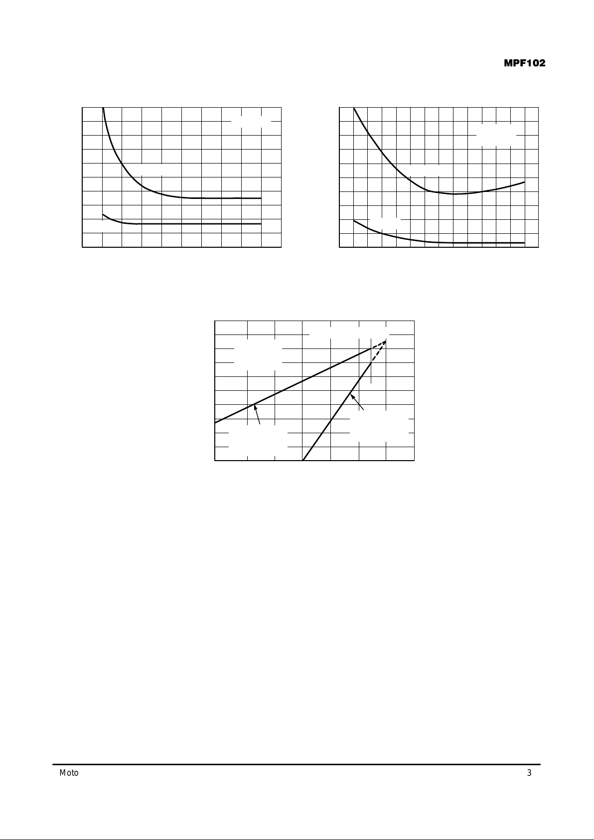
 Loading...