

Page 1
SEMICONDUCTOR TECHNICAL DATA
1
REV 0
Motorola, Inc. 1997
9/97
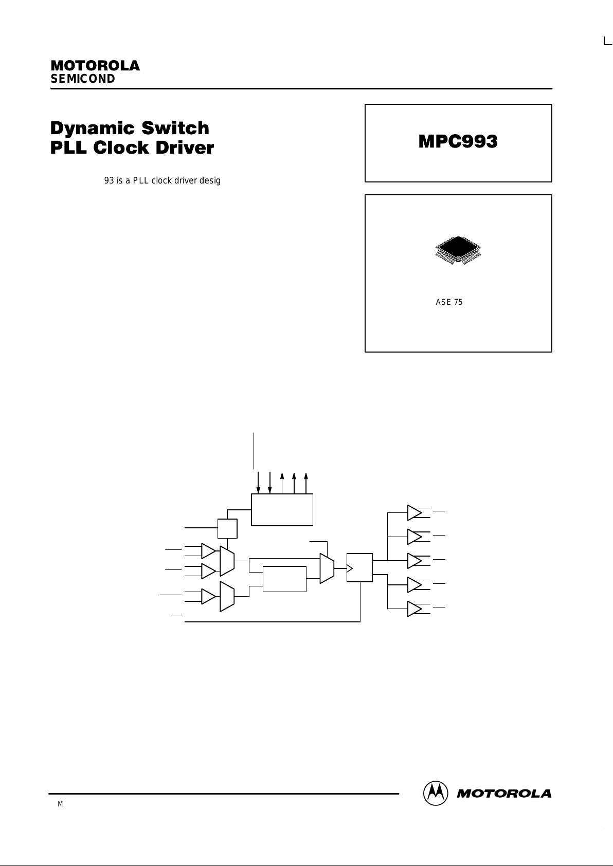
The MPC993 is a PLL clock driver designed specifically for redundant
clock tree designs. The device receives two differential LVPECL clock
signals from which it generates 5 new differential LVPECL clock outputs.
Two of the output pairs regenerate the input signals frequency and phase
while the other three pairs generate 2x, phase aligned clock outputs.
External PLL feedback is used to also provide zero delay buffer
performance.
• Fully Integrated PLL
• Intelligent Dynamic Clock Switch
• LVPECL Clock Outputs
• LVCMOS Control/Statis I/O
• 3.3V Operation
• 32–Lead TQFP Packaging
• ±50ps Cycle–Cycle Jitter
The MPC993 continuously monitors the two input signals to identify faulty reference clocks. Upon identification of a faulty
input clock (input clock stuck HIGH or LOW for at least 3 feedback clock edges), an input bad flag will be set and the device will
automatically switch from the bad reference clock input to the good one. During this dynamic switch of the input references, the
MPC993 outputs will slew, with minimal period disturbances to the new phase.
Figure 1. Block Diagram
CLK0
CLK0
CLK1
CLK1
Ext_FB
Ext_FB
OR
Sel_Clk
Dynamic Switch
Logic
PLL
PLL_En
÷
2
÷
4
Qb0
Qb0
Qb1
Qb1
Qb2
Qb2
Qa0
Qa0
Qa1
Qa1
MR
Man_OVerride
Alarm_Reset
Inp0bad
Inp1bad
Clk_Selected
FA SUFFIX
32–LEAD PLASTIC TQFP PACKAGE
CASE 751D–04
Page 2
MPC993
MOTOROLA ECLinPS and ECLinPS Lite
DL140 — Rev 3
2
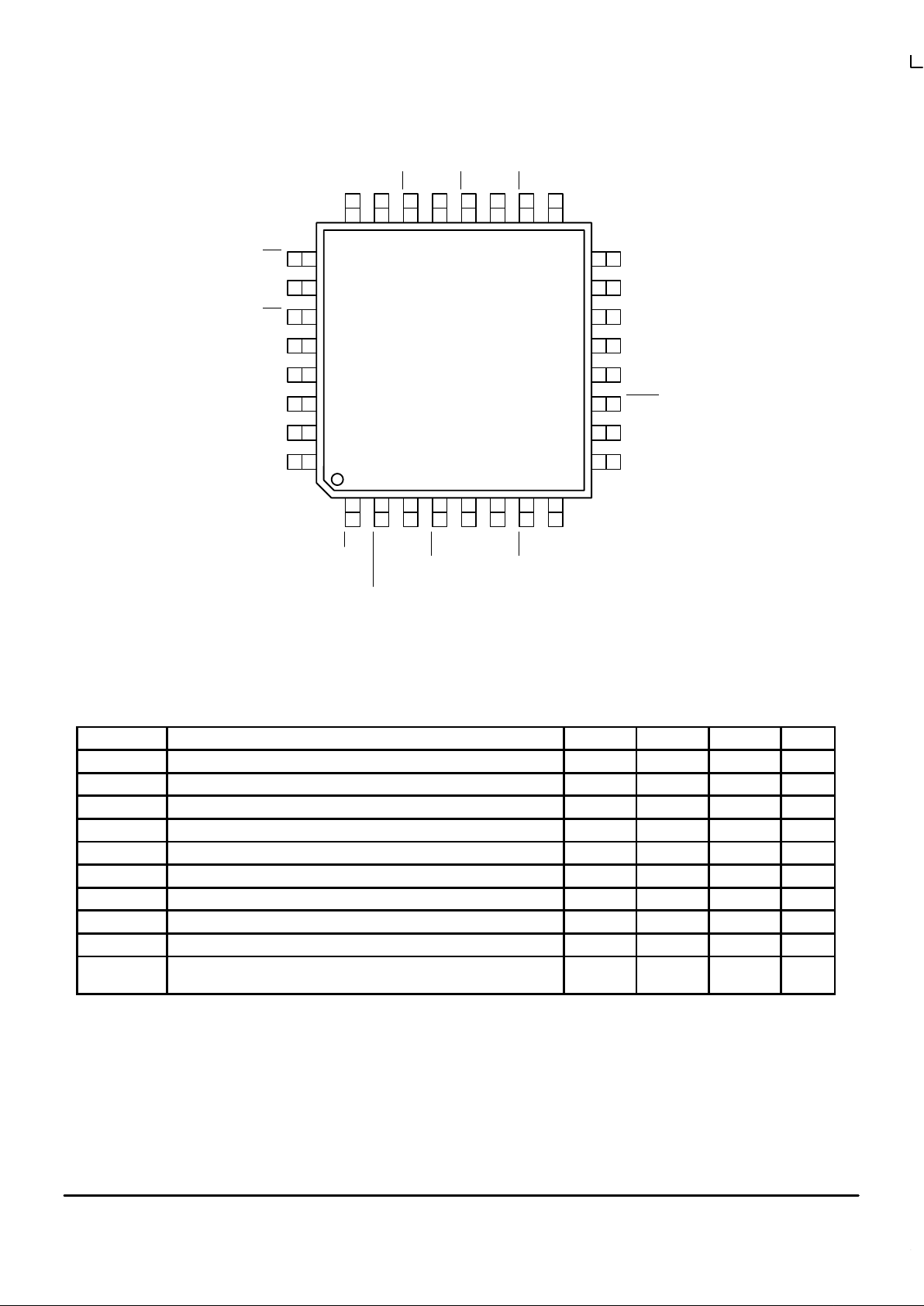
Figure 2. 32–Lead Pinout (Top View)
GND
VCC
Qb0
Qb0
Qb1
Qb1
Qb2
Qb2
VCC
MR
Alarm_Reset
CLK0
CLK0
Sel_Clk
CLK1
CLK1
GNDA
25
26
27
28
29
30
31
32
15
14
13
12
11
10
9
12345678
24 23 22 21 20 19 18 17
16
PRELIMINARY
MPC993
Ext_FB
Ext_FB
GND
Clk_Selected
Inp1bad
Inp0bad
VCC
PLL_En
Man_Override
VCCA
VCC
Qa0
Qa0
Qa1
Qa1
3.3V PECL DC Characteristics (TA = 0°C to 70°C)
Symbol Parameter Min Typ Max Unit
V
OH
Output HIGH Voltage (LVPECL Outputs) 2.275 2.345 2.420 V
V
OH
Output HIGH Voltage (LVCMOS Outputs) 2.4 V
V
OL
Output LOW Voltage (LVPECL Outputs) 1.490 1.595 1.680 V
V
OL
Output LOW Voltage (LVCMOS Outputs) 0.5 V
V
IH
Input HIGH Voltage (LVPECL Outputs) 2.135 2.420 V
V
IH
Input HIGH Voltage (LVCMOS Outputs) 2.0 3.3 V
V
IL
Input LOW Voltage (LVPECL Outputs) 1.490 1.825 V
V
IL
Input LOW Voltage (LVCMOS Outputs) 0.8 V
I
IL
Input LOW Current 0.5 µA
I
EE
Power Supply Current GNDA
GND
15
80
mA
Page 3

MPC993
3 MOTOROLAECLinPS and ECLinPS Lite
DL140 — Rev 3
3.3V PECL AC Characteristics (TA = 0°C to 85°C)
Symbol Parameter Min Typ Max Unit
f
VCO
Maximum VCO Frequency 480 MHz
t
pwi
25 75 %
t
pd
Propagation Delay (Note 1.) CLKn to Q (Bypass)
CLKn to Q (Locked (Note 2.))
X–500
Y–150
2000
0
X+500
Y+150
ps
tr/t
f
Output Rise/Fall Time 200 800 ps
t
skew
Output Skew Within Bank
All Outputs
50
100
ps
∆
pe
Maximum Phase Error Deviation TBD (Note 3.)
TBD (Note 4.)
ps
∆
per/cycle
Rate of Change of Periods 75MHz Output (Note 3.)
150MHz Output (Note 3.)
75MHz Output (Note 4.)
150MHz Output (Note 4.)
20
10
TBD
TBD
ps
t
pw
Output Duty Cycle 45 55 %
t
jitter
Cycle–to–Cycle Jitter 50 ps
t
lock
Maximum PLL Lock Time 10 ms
1. These values represent simulation results. Final values will be determined from silicon measurements and may be adjusted slightly.
2. Static phase offset between the selected reference clock and the feedback signal.
3. Specification holds for a clock switch between two signals no greater than 400ps out of phase. Delta period change per cycle is averaged over
the clock switch excursion. (See Applications Information section on page 4 for more detail)
4. Specification holds for a clock switch between two signals no greater than ±π out of phase. Delta period change per cycle is averaged over the
clock switch excursion.
PIN DESCRIPTIONS
Pin Name I/O Pin Definition
CLK0, CLK0
CLK1, CLK1
LVPECL Input
LVPECL Input
Differential PLL clock reference (CLK0 pulldown, CLK0 pullup)
Differential PLL clock reference (CLK1 pulldown, CLK1
pullup)
Ext_FB, Ext_FB LVPECL Input Differential PLL feedback clock (Ext_FB pulldown, Ext_FB pullup)
Qa0:1, Qa0:1 LVPECL Output Differential 1x output pairs
Qb0:2, Qb0:2 LVPECL Output Differential 2x output pairs
Inp0bad LVCMOS Output Indicates detection of a bad input reference clock 0 with respect to the feedback signal. The output
is active HIGH and will remain HIGH until the alarm reset is asserted
Inp1bad LVCMOS Output Indicates detection of a bad input reference clock 1 with respect to the feedback signal. The output
is active HIGH and will remain HIGH until the alarm reset is asserted
Clk_Selected LVCMOS Output ‘0’ if clock 0 is selected, ‘1’ if clock 1 is selected
Alarm_Reset LVCMOS Input ‘0’ will reset the input bad flags and align Clk_Selected with Sel_Clk. The input is “one–shotted”
(75Ω pullup)
Sel_Clk L VCMOS Input ‘0’ selects CLK0, ‘1’ selects CLK1 (75Ω pulldown)
Manual_Override L VCMOS Input ‘1’ disables internal clock switch circuitry (75Ω pulldown)
PLL_En LVCMOS Input ‘0’ bypasses selected input reference around the phase–locked loop (75Ω pulldown)
MR LVCMOS Input ‘0’ resets the internal dividers forcing Q outputs LOW. Asynchronous to the clock (75Ω pullup)
VCCA Power Supply PLL power supply
VCC Power Supply Digital power supply
GNDA Power Supply PLL ground
GND Power Supply Digital ground
Page 4

MPC993
MOTOROLA ECLinPS and ECLinPS Lite
DL140 — Rev 3
4
The MPC993 is a single switch circuit. The device
continuously monitors the two input signals to identify faulty
reference clocks. A clock is considered faulty if it has been
stuck LOW or HIGH for 3 consecutive feedback clock edges
(rising or falling). Upon identifying a faulty reference clock, an
input bad flag (Inp0bad or Inp1bad) corresponding to the
faulty clock will be set. If the PLL was currently locked to the
input signal that goes bad, the MPC993 will automatically
switch to the other clock provided it is operational. The input
bad flags will remain set until an Alarm_Reset
is asserted.
The Alarm_Reset
input is an active LOW input that will reset
the input bad flag(s). Note that the Alarm_Reset
is one
shotted, thus if upon clearing the input bad flags the inputs
are still bad the flags will be reset without the Alarm_Reset
pin being negated.
If both of the input signals go bad simultaneously the
MPC993 PLL will lose lock and the VCO will drift to an
indeterminate frequency. Once the MPC993 switches from a
bad clock it will continue to use the new clock until the
Alarm_Reset
pin is asserted. The device will not switch back
to a “repaired” bad input clock until the Alarm_Reset
is
asserted. Asserting the Alarm_Reset
pin forces the
Clk_Selected output to match the Sel_Clk input. Users
identify their primary clock via the Sel_Clk input. If not faulty
the MPC993 will always lock to this clock source in the
normal mode of operation. The only time clock Clk_Selected
does not equal Sel_Clk is when the device is in automatic
switch mode and the primary clock source is faulty. In this
condition the MPC993 will have switched to the secondary
clock and Clk_Selected will be in the opposite state as
Sel_Clk. Note that when in manual override (Man_Override
input is asserted) Clk_Selected will always equal Sel_Clk
regardless of the condition of the input bad flags.
Upon detection and switch from a “bad” input to a “good”
one, the internal PLL of the MPC993 will ensure a smooth
phase transition from the original to the new reference clock
source. The magnitudes of the disturbances seen in the
output clocks are detailed in the AC tables of this data sheet.
The two datasheet specifications are the maximum phase
error deviation and the rate of change of the output periods
during a reference clock switch. The maximum phase error
deviation describes the change in the input/output phase
difference caused by a switch between two out–of–phase
references. The rate of change periods describes the
behavior of the output signals from the MPC993 as it requires
phase–lock to the new reference source. Two different
conditions are specified, one for a maximum phase deviation
of the two clock sources of ≤±400ps and the other for phase
deviations of ≤±π. Under these conditions the MPC993 will be
guaranteed to take the “shortest path” to regain phase lock.
That is for a phase difference of –300ps, the output phase will
slew 300ps to align to the new phase as opposed to travelling
one clock period minus 300ps in the other direction. This
guarantee will ensure phase coherency in a clocking scheme
in which multiple MPC993’s are synchronized in a clock tree
and a subset of the devices under go a dynamic switch. Note
if the phase of the two input clock sources differs by more
than ±π the direction of phase lock cannot be guaranteed.
To calculate the overall uncertainty between any clocks
from multiple MPC993’s the following procedure should be
followed. Assuming that the reference clocks to the multiple
MPC993’s are exactly in phase, the total uncertainty will be
the combination of the static phase offset uncertainty
between the reference and feedback clocks, plus the
uncertainty between the feedback clock and the other clock
outputs, plus the jitter between the reference clock and
feedback clock inputs to the PLL. Based on the preliminary
data sheet specifications on this data sheet the total
uncertainty between CPU clocks would be 300ps + 50ps +
200ps or 550ps. The numbers used to derive this are the
Tpd, Output Skew and I/O jitter numbers respectively. Any
uncertainty in the phase of the reference clocks between the
different MPC993’s will add directly to this calculated
uncertainty.
During a dynamic switch the part to part skew between
two devices may be increased for a short period of time. In
the condition that only a subset of a number of parallel
MPC993’s under go a dynamic switch an additional
component will need to be added to the part to part skew of
the device during this transient event. If the two reference
clocks are 400ps out of phase a dynamic switch of an
MPC993 will lead to an instantaneous change of the input
phase by 400ps without a corresponding change in the
output phase due to the limited bandwidth of the PLL. As a
result the delay through a device under going the above
described switch will change by 400ps until the PLL has an
opportunity to slew to its new phase. This transient timing
issue should be considered when analyzing the overall skew
budget of a system.
The MPC993 inputs are not designed for “hot insertion”
applications when the device is used in a PECL environment.
In an ECL environment the reference clock inputs to the
device are hot insertion compatible. However in a PECL
environment a powered down receiver will present a low
impedance connection to ground to a powered up driver. To
make the MPC993 hot insertion compatible in a PECL
environment series resistance needs to be added in front of
the input reference clock pins to limit the current in the above
mentioned case. For a 3.3V PECL environment a 100Ω
series resistor will be sufficient to limit the current to
acceptable levels for both the driver and the receiver. A 100Ω
series resistor on the reference clock inputs will have minimal
impact on the rise and fall times of the input signals.
Page 5

MPC993
5 MOTOROLAECLinPS and ECLinPS Lite
DL140 — Rev 3
OUTLINE DIMENSIONS
FA SUFFIX
PLASTIC TQFP PACKAGE
CASE 873A–02
ISSUE A
DETAIL Y
A
S1
VB
1
8
9
17
25
32
AE
AE
P
DETAIL Y
BASE
N
J
DF
METAL
SECTION AE–AE
G
SEATING
PLANE
R
Q
_
W
K
X
0.250 (0.010)
GAUGE PLANE
E
C
H
DETAIL AD
NOTES:
1. DIMENSIONING AND TOLERANCING PER ANSI
Y14.5M, 1982.
2. CONTROLLING DIMENSION: MILLIMETER.
3. DATUM PLANE –AB– IS LOCATED AT BOTTOM OF
LEAD AND IS COINCIDENT WITH THE LEAD
WHERE THE LEAD EXITS THE PLASTIC BODY AT
THE BOTTOM OF THE PARTING LINE.
4. DATUMS –T–, –U–, AND –Z– TO BE DETERMINED
AT DATUM PLANE –AB–.
5. DIMENSIONS S AND V TO BE DETERMINED AT
SEATING PLANE –AC–.
6. DIMENSIONS A AND B DO NOT INCLUDE MOLD
PROTRUSION. ALLOWABLE PROTRUSION IS
0.250 (0.010) PER SIDE. DIMENSIONS A AND B
DO INCLUDE MOLD MISMATCH AND ARE
DETERMINED AT DATUM PLANE –AB–.
7. DIMENSION D DOES NOT INCLUDE DAMBAR
PROTRUSION. DAMBAR PROTRUSION SHALL
NOT CAUSE THE D DIMENSION TO EXCEED
0.520 (0.020).
8. MINIMUM SOLDER PLATE THICKNESS SHALL BE
0.0076 (0.0003).
9. EXACT SHAPE OF EACH CORNER MAY VARY
FROM DEPICTION.
DIMAMIN MAX MIN MAX
INCHES
7.000 BSC 0.276 BSC
MILLIMETERS
B 7.000 BSC 0.276 BSC
C 1.400 1.600 0.055 0.063
D 0.300 0.450 0.012 0.018
E 1.350 1.450 0.053 0.057
F 0.300 0.400 0.012 0.016
G 0.800 BSC 0.031 BSC
H 0.050 0.150 0.002 0.006
J 0.090 0.200 0.004 0.008
K 0.500 0.700 0.020 0.028
M 12 REF 12 REF
N 0.090 0.160 0.004 0.006
P 0.400 BSC 0.016 BSC
Q 1 5 1 5
R 0.150 0.250 0.006 0.010
V 9.000 BSC 0.354 BSC
V1 4.500 BSC 0.177 BSC
__
____
DETAIL AD
A1
B1
V1
4X
S
4X
B1 3.500 BSC 0.138 BSC
A1 3.500 BSC 0.138 BSC
S 9.000 BSC 0.354 BSC
S1 4.500 BSC 0.177 BSC
W 0.200 REF 0.008 REF
X 1.000 REF 0.039 REF
9
–T–
–Z–
–U–
T–U0.20 (0.008) ZAC
T–U0.20 (0.008) ZAB
0.10 (0.004) AC
–AC–
–AB–
M
_
8X
–T–, –U–, –Z–
T–U
M
0.20 (0.008) ZAC
Page 6

MPC993
MOTOROLA ECLinPS and ECLinPS Lite
DL140 — Rev 3
6
Motorola reserves the right to make changes without further notice to any products herein. Motorola makes no warranty , representation or guarantee regarding
the suitability of its products for any particular purpose, nor does Motorola assume any liability arising out of the application or use of any product or circuit, and
specifically disclaims any and all liability, including without limitation consequential or incidental damages. “T ypical” parameters which may be provided in Motorola
data sheets and/or specifications can and do vary in different applications and actual performance may vary over time. All operating parameters, including “Typicals”
must be validated for each customer application by customer’s technical experts. Motorola does not convey any license under its patent rights nor the rights of
others. Motorola products are not designed, intended, or authorized for use as components in systems intended for surgical implant into the body, or other
applications intended to support or sustain life, or for any other application in which the failure of the Motorola product could create a situation where personal injury
or death may occur. Should Buyer purchase or use Motorola products for any such unintended or unauthorized application, Buyer shall indemnify and hold Motorola
and its officers, employees, subsidiaries, affiliates, and distributors harmless against all claims, costs, damages, and expenses, and reasonable attorney fees
arising out of, directly or indirectly, any claim of personal injury or death associated with such unintended or unauthorized use, even if such claim alleges that
Motorola was negligent regarding the design or manufacture of the part. Motorola and are registered trademarks of Motorola, Inc. Motorola, Inc. is an Equal
Opportunity/Affirmative Action Employer.
MPC993/D
◊
Mfax is a trademark of Motorola, Inc.
How to reach us:
USA/EUROPE/Locations Not Listed: Motorola Literature Distribution; JAPAN: Nippon Motorola Ltd.: SPD, Strategic Planning Office, 4–32–1,
P.O. Box 5405, Denver, Colorado 80217. 1–303–675–2140 or 1–800–441–2447 Nishi–Gotanda, Shinagawa–ku, Tokyo 141, Japan. 81–3–5487–8488
Customer Focus Center: 1–800–521–6274
Mfax: RMFAX0@email.sps.mot.com – TOUCHTONE 1–602–244–6609 ASIA/PACIFIC: Motorola Semiconductors H.K. Ltd.; 8B Tai Ping Industrial Park,
Moto rola Fax Back System – US & Canada ONLY 1–800–774–1848 51 Ting Kok Road, Tai Po, N.T., Hong Kong. 852–26629298
– http://sps.motorola.com/mfax/
HOME PAGE: http://motorola.com/sps/
 Loading...