

Page 1
SEMICONDUCTOR TECHNICAL DATA
1
REV 1
Motorola, Inc. 1996
7/96
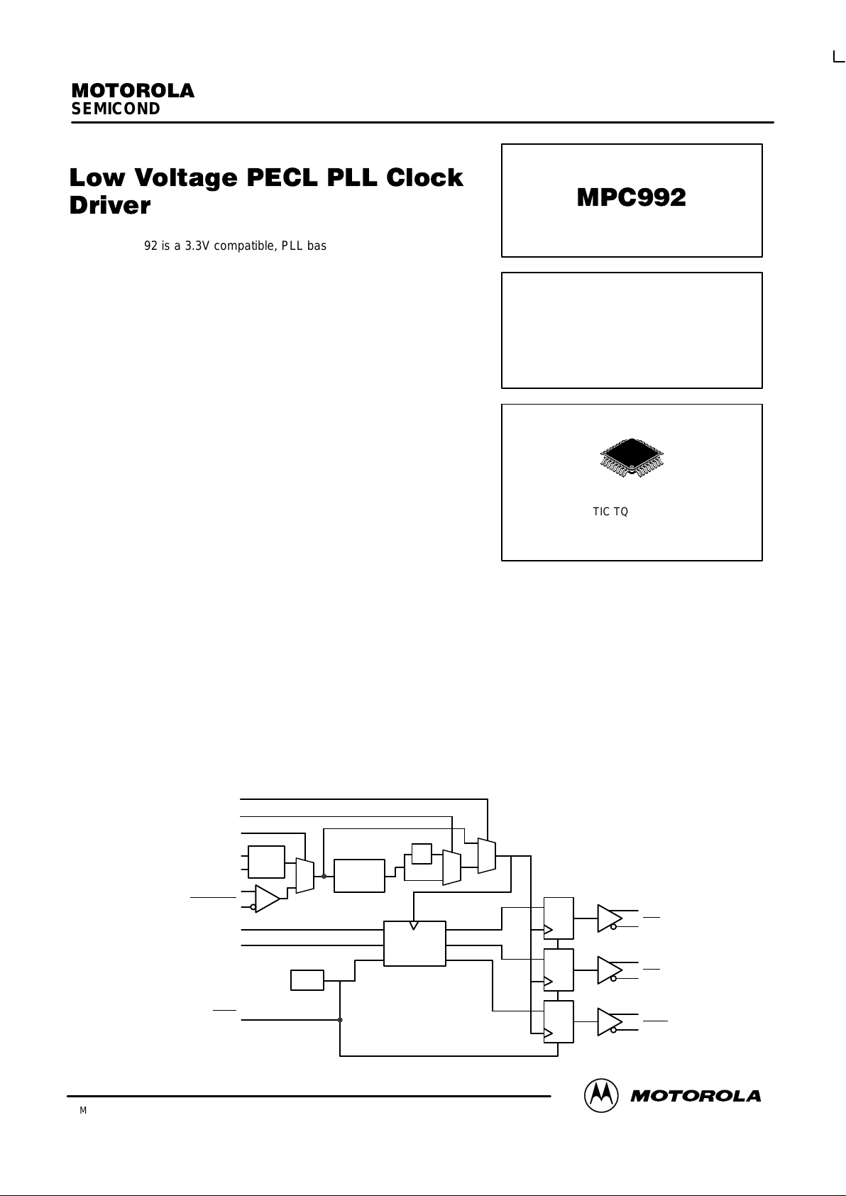
The MPC992 is a 3.3V compatible, PLL based PECL clock generator
and distributor. The fully differential design ensures optimum skew and
PLL jitter performance. The performance of the device makes the
MPC992 ideal for workstations, main frame computer, telecommunication
and instrumentation applications. The device offers a crystal oscillator or
a differential PECL reference clock input to provide flexibility in the
reference clock interface. All of the control signals to the MPC992 are
LVTTL compatible inputs.
• Fully Integrated PLL
• Output Frequency of up to 400MHz
• PECL Clock Inputs and Outputs
• Operates from a 3.3V V
CC
Supply
• Output Frequency Configurable
• 32 TQFP Packaging
• ±25ps Cycle–Cycle Jitter
The MPC992 offers two banks of outputs which can be configured into
four different relationships. The output banks can be configured into 2:1,
3:1, 3:2 and 5:2 ratios to provide a wide variety of potential frequency
outputs. In addition to these two banks of outputs a synchronization output is also offered. The SYNC output will provide
information as to the time when the two output banks will transition positively in phase. This information can be important when
the odd ratios are used as it provides for a baseline point in the system timing. The SYNC output will pulse high for one Qa clock
period, centered on the rising Qa clock edge four edges prior to the Qb synchronous edge. The relationship is illustrated in the
timing diagrams in the data sheet.
The MPC992 offers several features to aid in system debug and test. The PECL reference input pins can be interfaced to a test
signal and the PLL can be bypassed to allow the designer to drive the MPC992 outputs directly. This allows for single stepping in
a system functional debug mode. In addition an overriding reset is provided which will force all of the Q outputs LOW upon
assertion.
The MPC992 is packaged in a 32–lead TQFP package to optimize both performance and board density.
Qan
Qan
(x4)
Qbn
Qbn
(x3)
SYNC
SYNC
(x1)
Frequency
Generator
PLL_EN
PECL_CLK
PECL_CLK
XTAL_SEL
XTAL
OSC
XTAL1
XTAL2
VCO_SEL
Integrated
PLL
x2
FSEL0
FSEL1
POR
Reset
MPC992 LOGIC DIAGRAM
1
0
0
1
0
1
LOW VOLTAGE
PLL CLOCK DRIVER
FA SUFFIX
PLASTIC TQFP PACKAGE
CASE 873A-02
Page 2
MPC992
MOTOROLA TIMING SOLUTIONS
BR1333 — REV 5
2
Qb1
Qb2
Qa1
Qa1
Qa0
GNDA
VCCA
VCCI
Qb0
Qb1
Qb2
PLL_EN
GNDI
VCCO1
Qa2
Qa2
Qa3
Qa3
SYNC
SYNC
VCCO2
VCO_SEL
FSEL0
FSEL1
XTAL_SEL
PECL_CLK
PECL_CLK
XTAL1
XTAL2
25
26
27
28
29
30
31
32
15
14
13
12
11
10
9
12345678
24 23 22 21 20 19 18 17
16
MPC992
Reset
Qa0
Qb0
FUNCTION TABLE 1
FSEL0 FSEL1 Qa Qb Feedback Ratio
0
0
1
1
0
1
0
1
VCO/4
VCO/2
VCO/4
VCO/2
VCO/6
VCO/4
VCO/10
VCO/6
VCO/24
VCO/16
VCO/40
VCO/24
3:2
2:1
5:2
3:1
INPUT vs OUTPUT FREQUENCY
FSEL0 FSEL1 Qa Qb Int Feedback
0
0
1
1
0
1
0
1
6 (f
ref
)
8 (f
ref
)
10 (f
ref
)
12 (f
ref
)
4 (f
ref
)
4 (f
ref
)
4 (f
ref
)
4 (f
ref
)
f
ref
f
ref
f
ref
f
ref
FUNCTION TABLE 2
Control Signal Logic ‘0’ Logic ‘1’
Reset Outputs Enabled Outputs Disabled
XTAL_SEL PECL REF XTAL REF
PLL_EN Disabled Enabled
VCO_SEL High Frequency Low Frequency
PIN DESCRIPTION
Pin Name Function
VCO_SEL VCO range select pin (Int Pullup)
PLL_EN PLL bypass select pin (Int Pullup)
XTAL_SEL Input reference source select pin (Int Pullup)
XTAL1:2 Crystal interface pins for the internal oscillator
PECL_CLK True PECL reference clock input (Int Pulldown)
PECL_CLK
Compliment PECL reference clock input
(Int Pullup)
FSELn Internal divider select pins (Int Pullup)
RESET
Internal flip–flop reset, true outputs go LOW
(Int Pulldown)
Page 3
MPC992
TIMING SOLUTIONS
BR1333 — REV 5
3 MOTOROLA
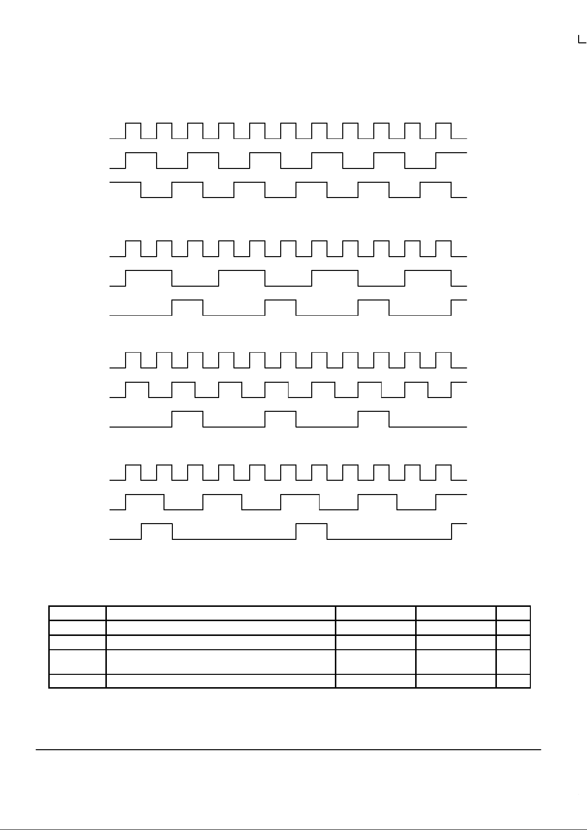
Figure 1. Output Waveforms
Qa
2:1 Mode
Qb
SYNC
Qa
3:1 Mode
Qb
SYNC
Qa
3:2 Mode
Qb
SYNC
5:2 Mode
Qa
Qb
SYNC
ABSOLUTE MAXIMUM RATINGS*
Symbol Parameter Min Max Unit
V
CC
Supply Voltage –0.3 4.6 V
V
I
Input Voltage –0.3 VDD + 0.3 V
I
OUT
Output Current Continuous
Surge
50
100
mA
T
Stor
Storage Temperature Range –40 125 °C
* Absolute maximum continuous ratings are those values beyond which damage to the device may occur. Exposure to these conditions or
conditions beyond those indicated may adversely affect device reliability. Functional operation under absolute-maximum-rated conditions is not
implied.
Page 4

MPC992
MOTOROLA TIMING SOLUTIONS
BR1333 — REV 5
4
DC CHARACTERISTICS (TA = 0° to 70°C, VCC = 3.3V ±5%)
Symbol Characteristic Min Typ Max Unit Condition
V
IH
Input HIGH Voltage PECL_CLK
1
Other
2.15
2.0
2.4
V
CC
V VCC = 3.3V
V
IL
Input LOW Voltage PECL_CLK
1
Other
1.5
0
1.8
0.8
V VCC = 3.3V
V
OH
Output HIGH Voltage
1
1.8 2.4 V VCC = 3.3V
V
OL
Output LOW Voltage
1
1.2 1.7 V VCC = 3.3V
I
IN
Input Current –120 120 µA
I
CCI
Maximum Quiescent Supply Current 130 150 mA
I
CCA
Maximum PLL Supply Current 15 20 mA
1. DC levels will vary 1:1 with VCC.
AC CHARACTERISTICS (TA = 0° to 70°C, VCC = 3.3V ±5%)
Symbol Characteristic Min Typ Max Unit Condition
tr, t
f
Output Rise/Fall Time 200 850 ps 20% to 80%
t
pw1
Output Duty Cycle 49 51 %
t
pw2
SYNC Output Duty Cycle 0.95 1.05 % PCLK Period
f
ref
Input Reference Frequency Xtal
FREF10Note 2
20
Note 2
MHz
t
os
Output-to-Output Skew Qa, Qb
Qa (–) to SYNC (+)
100
300
ps
f
VCO
PLL VCO Lock Range 200
400
440
750
MHz VCO_SEL = 1
VCO_SEL = 0
f
max
Maximum Output Frequency Qa (÷2)
Qa,Qb (÷4)
Qb (÷6)
Qb (÷10)
375
187.5
125
75
MHz Note 1
t
jitter
Cycle–to–Cycle Jitter (Peak–to–Peak) ±25 ±50 ps Note 3
t
lock
Maximum PLL Lock Time 10 ms
1. At 400MHz the output swing will be less than the nominal value.
2. ECLK and XTAL input reference limited by the feedback divide and the guaranteed VCO lock range.
3. Guaranteed by characterization.
APPLICATIONS INFORMATION
Using the On–Board Crystal Oscillator
The MPC992 features an on–board crystal oscillator to
allow for seed clock generation as well as final distribution.
The on–board oscillator is completely self contained so that
the only external component required is the crystal. As the
oscillator is somewhat sensitive to loading on its inputs the
user is advised to mount the crystal as close to the MPC992
as possible to avoid any board level parasitics. To facilitate
co–location surface mount crystals are recommended, but
not required.
The oscillator circuit is a series resonant circuit as
opposed to the more common parallel resonant circuit, this
eliminates the need for large on–board capacitors. Because
the design is a series resonant design, for optimum
frequency accuracy a series resonant crystal should be used
(see specification table below). Unfortunately most off the
shelf crystals are characterized in a parallel resonant mode.
However a parallel resonant crystal is physically no different
than a series resonant crystal, a parallel resonant crystal is
simply a crystal which has been characterized in its parallel
resonant mode. Therefore in the majority of cases a parallel
specified crystal can be used with the MPC992 with just a
minor frequency error due to the actual series resonant
frequency of the parallel resonant specified crystal. Typically
Page 5

MPC992
TIMING SOLUTIONS
BR1333 — REV 5
5 MOTOROLA
a parallel specified crystal used in a series resonant mode
will exhibit an oscillatory frequency a few hundred ppm lower
than the specified value. For most processor implementa–
tions a few hundred ppm translates into kHz inaccuracies, a
level which does not represent a major issue.
Figure 2 shows an optional series capacitor in the crystal
oscillator interface. The on–board oscillator introduces a
small phase shift in the overall loop which causes the
oscillator to operate at a frequency slightly slower than the
specified crystal. The series capacitor is used to compensate
the loop and allow the oscillator to function at the specified
crystal frequency. If a 100ppm type error is not important, the
capacitor can be left off the PCB. For more detailed
information, order Motorola Application Note AN1579/D.
Figure 2. Recommended Crystal Interface
XTAL2
C
TUNE
(Optional)
XTAL1
MPC992
Table 1. Crystal Specifications
Parameter Value
Crystal Cut Fundamental AT Cut
Resonance Series Resonance*
Frequency Tolerance ±75ppm at 25°C
Frequency/Temperature Stability ±150ppm 0 to 70°C
Operating Range 0 to 70° C
Shunt Capacitance 5–7pF
Equivalent Series Resistance (ESR) 50 to 80Ω max
Correlation Drive Level 100µW
Aging 5ppm/Yr (First 3 Y ears)
Power Supply Filtering
The MPC992 is a mixed analog/digital product and as
such it exhibits some sensitivities that would not necessarily
be seen on a fully digital product. Analog circuitry is naturally
susceptible to random noise, especially if this noise is seen
on the power supply pins. The MPC992 provides separate
power supplies for the digital circuitry (V
CCI
) and the internal
PLL (VCCA) of the device. The purpose of this design
technique is to try and isolate the high switching noise digital
outputs from the relatively sensitive internal analog
phase–locked loop. In a controlled environment such as an
evaluation board this level of isolation is sufficient. However,
in a digital system environment where it is more difficult to
minimize noise on the power supplies a second level of
isolation may be required. The simplest form of isolation is a
power supply filter on the VCCA pin for the MPC992.
Figure 3 illustrates a typical power supply filter scheme.
The MPC992 is most susceptible to noise with spectral
content in the 10kHz to 1MHz range. Therefore the filter
should be designed to target this range. The key parameter
that needs to be met in the final filter design is the DC voltage
drop that will be seen between the VCC supply and the VCCA
pin of the MPC992. From the data sheet the I
VCCA
current
(the current sourced through the VCCA pin) is typically 15mA
(20mA maximum), assuming that a minimum of 3.0V must be
maintained on the VCCA pin very little DC voltage drop can
be tolerated when a 3.3V VCC supply is used. The resistor
shown in Figure 3 must have a resistance of 10–15Ω to meet
the voltage drop criteria. The RC filter pictured will provide a
broadband filter with approximately 100:1 attenuation for
noise whose spectral content is above 20KHz. As the noise
frequency crosses the series resonant point of an individual
capacitor it’s overall impedance begins to look inductive and
thus increases with increasing frequency. The parallel
capacitor combination shown ensures that a low impedance
path to ground exists for frequencies well above the
bandwidth of the PLL.
Figure 3. Power Supply Filter
VCCA
VCC
MPC992
0.01µF
22
µ
F
0.01
µ
F
3.3V
RS=10–15
Ω
A higher level of attenuation can be achieved by replacing
the resistor with an appropriate valued inductor. A 1000µH
choke will show a significant impedance at 10KHz
frequencies and above. Because of the current draw and the
voltage that must be maintained on the VCCA pin a low DC
resistance inductor is required (less than 15Ω). Generally the
resistor/capacitor filter will be cheaper, easier to implement
and provide an adequate level of supply filtering.
The MPC992 provides sub–nanosecond output edge
rates and thus a good power supply bypassing scheme is a
must. The important aspect of the layout for the MPC992 is
low impedance connections between VCC and GND for the
bypass capacitors. Combining good quality general purpose
chip capacitors with good PCB layout techniques will
produce effective capacitor resonances at frequencies
adequate to supply the instantaneous switching current for
the MPC992 outputs. It is imperative that low inductance chip
capacitors are used; it is equally important that the board
layout does not introduce back all of the inductance saved by
using the leadless capacitors. Thin interconnect traces
between the capacitor and the power plane should be
avoided and multiple large vias should be used to tie the
Page 6

MPC992
MOTOROLA TIMING SOLUTIONS
BR1333 — REV 5
6
capacitors to the buried power planes. Fat interconnect and
large vias will help to minimize layout induced inductance and
thus maximize the series resonant point of the bypass
capacitors.
No active signal lines should pass below the crystal
interface to the MPC992. The oscillator is a series resonant
circuit and the voltage amplitude across the crystal is
relatively small. It is imperative that no actively switching
signals cross under the crystal as crosstalk energy coupled
to these lines could significantly impact the jitter of the device.
Special attention should be paid to the layout of the crystal to
ensure a stable, jitter free interface between the crystal and
the on–board oscillator. In addition, the crystal interface
circuitry will be adversely affected by activity on the
PECL_CLK inputs. Therefore, it is recommended that the
PECL input signals be static when the crystal oscillator
circuitry is being used.
Although the MPC992 has several design features to
minimize the susceptibility to power supply noise (isolated
power and grounds and fully differential PLL) there still may
be applications in which overall performance is being
degraded due to system power supply noise. The power
supply filter and bypass schemes discussed in this section
should be adequate to eliminate power supply noise related
problems in most designs.
Page 7

MPC992
TIMING SOLUTIONS
BR1333 — REV 5
7 MOTOROLA
OUTLINE DIMENSIONS
FA SUFFIX
PLASTIC TQFP PACKAGE
CASE 873A-02
ISSUE A
DETAIL Y
A
S1
VB
1
8
9
17
25
32
AE
AE
P
DETAIL Y
BASE
N
J
DF
METAL
SECTION AE–AE
G
SEATING
PLANE
R
Q
_
W
K
X
0.250 (0.010)
GAUGE PLANE
E
C
H
DETAIL AD
NOTES:
1. DIMENSIONING AND TOLERANCING PER ANSI
Y14.5M, 1982.
2. CONTROLLING DIMENSION: MILLIMETER.
3. DATUM PLANE –AB– IS LOCATED AT BOTTOM OF
LEAD AND IS COINCIDENT WITH THE LEAD
WHERE THE LEAD EXITS THE PLASTIC BODY AT
THE BOTTOM OF THE PARTING LINE.
4. DATUMS –T–, –U–, AND –Z– TO BE DETERMINED
AT DATUM PLANE –AB–.
5. DIMENSIONS S AND V TO BE DETERMINED AT
SEATING PLANE –AC–.
6. DIMENSIONS A AND B DO NOT INCLUDE MOLD
PROTRUSION. ALLOWABLE PROTRUSION IS
0.250 (0.010) PER SIDE. DIMENSIONS A AND B
DO INCLUDE MOLD MISMATCH AND ARE
DETERMINED AT DATUM PLANE –AB–.
7. DIMENSION D DOES NOT INCLUDE DAMBAR
PROTRUSION. DAMBAR PROTRUSION SHALL
NOT CAUSE THE D DIMENSION TO EXCEED
0.520 (0.020).
8. MINIMUM SOLDER PLATE THICKNESS SHALL BE
0.0076 (0.0003).
9. EXACT SHAPE OF EACH CORNER MAY VARY
FROM DEPICTION.
DIMAMIN MAX MIN MAX
INCHES
7.000 BSC 0.276 BSC
MILLIMETERS
B 7.000 BSC 0.276 BSC
C 1.400 1.600 0.055 0.063
D 0.300 0.450 0.012 0.018
E 1.350 1.450 0.053 0.057
F 0.300 0.400 0.012 0.016
G 0.800 BSC 0.031 BSC
H 0.050 0.150 0.002 0.006
J 0.090 0.200 0.004 0.008
K 0.500 0.700 0.020 0.028
M 12 REF 12 REF
N 0.090 0.160 0.004 0.006
P 0.400 BSC 0.016 BSC
Q 1 5 1 5
R 0.150 0.250 0.006 0.010
V 9.000 BSC 0.354 BSC
V1 4.500 BSC 0.177 BSC
__
____
DETAIL AD
A1
B1
V1
4X
S
4X
B1 3.500 BSC 0.138 BSC
A1 3.500 BSC 0.138 BSC
S 9.000 BSC 0.354 BSC
S1 4.500 BSC 0.177 BSC
W 0.200 REF 0.008 REF
X 1.000 REF 0.039 REF
9
–T–
–Z–
–U–
T–U0.20 (0.008) ZAC
T–U0.20 (0.008) ZAB
0.10 (0.004) AC
–AC–
–AB–
M
_
8X
–T–, –U–, –Z–
T–U
M
0.20 (0.008) ZAC
Page 8

MPC992
MOTOROLA TIMING SOLUTIONS
BR1333 — REV 5
8
Motorola reserves the right to make changes without further notice to any products herein. Motorola makes no warranty , representation or guarantee regarding
the suitability of its products for any particular purpose, nor does Motorola assume any liability arising out of the application or use of any product or circuit, and
specifically disclaims any and all liability, including without limitation consequential or incidental damages. “T ypical” parameters which may be provided in Motorola
data sheets and/or specifications can and do vary in different applications and actual performance may vary over time. All operating parameters, including “Typicals”
must be validated for each customer application by customer’s technical experts. Motorola does not convey any license under its patent rights nor the rights of
others. Motorola products are not designed, intended, or authorized for use as components in systems intended for surgical implant into the body, or other
applications intended to support or sustain life, or for any other application in which the failure of the Motorola product could create a situation where personal injury
or death may occur. Should Buyer purchase or use Motorola products for any such unintended or unauthorized application, Buyer shall indemnify and hold Motorola
and its officers, employees, subsidiaries, affiliates, and distributors harmless against all claims, costs, damages, and expenses, and reasonable attorney fees
arising out of, directly or indirectly, any claim of personal injury or death associated with such unintended or unauthorized use, even if such claim alleges that
Motorola was negligent regarding the design or manufacture of the part. Motorola and are registered trademarks of Motorola, Inc. Motorola, Inc. is an Equal
Opportunity/Affirmative Action Employer.
How to reach us:
USA/EUROPE/Locations Not Listed: Motorola Literature Distribution; JAPAN: Nippon Motorola Ltd.; Tatsumi–SPD–JLDC, 6F Seibu–Butsuryu–Center,
P.O. Box 20912; Phoenix, Arizona 85036. 1–800–441–2447 or 602–303–5454 3–14–2 Tatsumi Koto–Ku, Tokyo 135, Japan. 03–81–3521–8315
MFAX: RMF AX0@email.sps.mot.com – T OUCHTONE 602–244–6609 ASIA / PACIFIC: Motorola Semiconductors H.K. Ltd.; 8B Tai Ping Industrial Park,
INTERNET: http://Design–NET.com 51 Ting Kok Road, Tai Po, N.T., Hong Kong. 852–26629298
MPC992/D
*MPC992/D*
◊
 Loading...