

Page 1
SEMICONDUCTOR TECHNICAL DATA
1
REV 2
Motorola, Inc. 1997
2/97
The MPC990/991 is a 3.3V compatible, PLL based ECL/PECL clock
driver. The fully differential design ensures optimum skew and PLL jitter
performance. The performance of the MPC990/991 makes the device
ideal for Workstation, Mainframe Computer and Telecommunication
applications. The MPC990 and MPC991 devices are identical except in
the interface to the reference clock for the PLL. The MPC990 offers an
on–board crystal oscillator as the PLL reference while the MPC991 offers
a differential ECL/PECL input for applications which need to lock to an
existing clock signal. Both designs offer a secondary single–ended ECL
clock for system test capabilities.
• Fully Integrated PLL
• Output Frequency Up to 400MHz
• ECL/PECL Inputs and Outputs
• Operates from a 3.3V Supply
• Output Frequency Configurable
• TQFP Packaging
• ±50ps Cycle–to–Cycle Jitter
The MPC990/991 offers three banks of outputs which can each be
programmed via the the four fsel pins of the device. There are 16 different
output frequency configurations available in the device. The
configurations include output ratios of 1:1, 2:1, 3:1, 3:2, 4:1, 4:3, 4:3:1 and
4:3:2. The programming table in this data sheet illustrates the various
programming options. The SYNC output monitors the relationship
between the Qa and Qc output banks. The output pulses per the timing
diagrams in this data sheet signal the coincident edges of the two output
banks. This feature is useful for non binary relationships between output frequencies (i.e., 3:2 or 4:3 relationships). The Sync_Sel
input toggles the Qd outputs between sync signals and extensions to the Qc bank of outputs.
The MPC990/991 provides a separate output for the feedback to the PLL. This allows for the feedback frequency to be
programmed independently of the other outputs allowing for unique input vs output frequency relationships. The fselFB inputs
provide 6 different feedback frequencies from the QFB differential output pair.
The MPC990/991 features an external differential ECL/PECL feedback to the PLL. This external feedback feature allows for
the MPC991’s use as a “zero” delay buffer. The propagation delay between the input reference and the output is dependent on
the input reference frequency. The selection of higher reference frequencies will provide near zero delay through the device.
The PLL_En, Ref_Sel and the Test_Clk input pins provide a means of bypassing the PLL and driving the output buffers
directly. This allows the user to single step a design during system debug. Note that the Test_Clk input is routed through the
dividers so that depending on the programming several edges on the Test_Clk input will be needed to get corresponding edge
transitions on the outputs. The VCO_Sel input provides a means of recentering the VCO to provide a broader range of VCO
frequencies for stable PLL operation.
If the frequency select or the VCO_Sel pins are changed during operation, a master reset signal must be applied to ensure
output synchronization and phase–lock. If the VCO is driven beyond its maximum frequency, the VCO can outrun the internal
dividers when the VCO_Sel pin is low. This will also prevent the PLL from achieving lock. Again, a master reset signal will need to
be applied to allow for phase–lock. The device employs a power–on reset circuit which will ensure output synchronization and
PLL lock on initial power–up.
LOW VOLTAGE
PLL CLOCK DRIVER
FA SUFFIX
52–LEAD TQFP PACKAGE
CASE 848D–03
Page 2

MPC990 MPC991
MOTOROLA TIMING SOLUTIONS
BR1333 — Rev 6
2
QFB
QFB
VCCO
Qd0
Qd0
Qd1
Qd1
VCCO
Qc0
Qc0
Qc1
Qc1
VCCA
fsel0
Qb2
Qb2
fsel1
Qb1
Qb1
fsel2
Qb0
Qb0
VCCO
Qc2
Qc2
fsel3
GNDI
MR
PLL_En
Ref_Sel
fselFB2
fselFB1
fselFB0
Test_Clk
VCCI
Ext_FB
xtal1 (990)
xtal2 (990)
Ext_FB
40
41
42
43
44
45
46
47
48
49
50
51
52
25
24
23
22
21
20
19
18
17
16
15
14
12345678910111213
39 38 37 36 35 34 33 32 31 30 29 28 27
26
MPC990/
MPC991
ECL_CLK (991)
ECL_CLK (991)
VCO_Sel
SYNC_Sel
Qa3
Qa3
Qa2
Qa2
Qa1
Qa1
Qa0
Qa0
VCCO
Qb3
Qb3
Figure 1. 52–Lead Pinout (Top View)
FUNCTION TABLE 1
INPUTS OUTPUTS
fsel3 fsel2 fsel1 fsel0 Qa Qb Qc
0 0 0 0 ÷2 ÷2 ÷2
0 0 0 1 ÷2 ÷2 ÷4
0 0 1 0 ÷2 ÷4 ÷4
0 0 1 1 ÷2 ÷2 ÷6
0 1 0 0 ÷2 ÷6 ÷6
0 1 0 1 ÷2 ÷4 ÷6
0 1 1 0 ÷2 ÷4 ÷8
0 1 1 1 ÷2 ÷6 ÷8
1 0 0 0 ÷2 ÷2 ÷8
1 0 0 1 ÷2 ÷8 ÷8
1 0 1 0 ÷4 ÷4 ÷6
1 0 1 1 ÷4 ÷6 ÷6
1 1 0 0 ÷4 ÷6 ÷8
1 1 0 1 ÷6 ÷6 ÷8
1 1 1 0 ÷6 ÷8 ÷8
1 1 1 1 ÷8 ÷8 ÷8
Page 3
MPC990 MPC991
TIMING SOLUTIONS
BR1333 — Rev 6
3 MOTOROLA
FUNCTION TABLE 2
fselFB2 fselFB1 fselFB0 QFB
0
0
0
0
0
0
1
1
0
1
0
1
÷2
÷4
÷6
÷8
1
1
1
1
0
0
1
1
0
1
0
1
÷8
÷16
÷24
÷32
FUNCTION TABLE 3
Control Pin Logic ‘0’ Logic ‘1’
PLL_En Enable PLL Bypass PLL
VCO_Sel fVCO fVCO/2
Ref_Sel xtal or ECL/PECL Test_Clk
MR — Reset Outputs
SYNC_Sel SYNC Outputs Match Qc Outputs
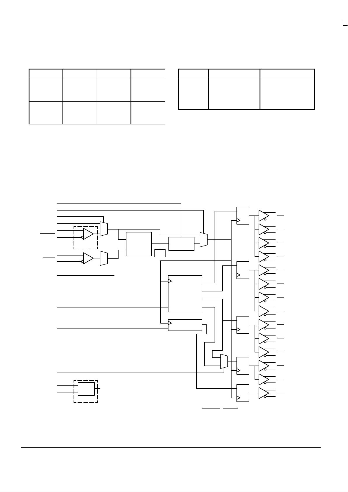
Figure 2. MPC990/991 Logic Diagram
VCO
PHASE
DETECTOR
LPF
PLL_En
VCO_Sel
ECL_Clk
ECL_Clk
Test_Clk
Ref_Sel
Ext_FB
Ext_FB
Qa0
Qa0
Qa1
Qa1
Qa2
Qa2
Qa3
Qa3
Qb0
Qb0
Qb1
Qb1
Qb2
Qb2
Qb3
Qb3
Qc0
Qc0
Qc1
Qc1
Qc2
Qc2
Qd0
Qd0
Qd1
Qd1
QFB
QFB
FREQUENCY
GENERATOR
SYNC
MR
fsela0:3
fselFB0:2
SYNC_Sel
(Pulldown)
(Pulldown)
(Pulldown)
(Pulldown)
(Pulldown)
(Pulldown)
(Pulldown)
(Pulldown)
MPC991
MPC990
Xtal
Osc
NOTE: ECL_Clk, Ext_FB have internal pulldowns, while ECL_Clk, Ext_FB have external
pullups to ensure stability under open input conditions.
Page 4

MPC990 MPC991
MOTOROLA TIMING SOLUTIONS
BR1333 — Rev 6
4
Figure 3. Timing Diagrams
Qa
1:1 Mode
Qc
Sync (Qd) V
CC
Qa
2:1 Mode
Qc
Sync (Qd)
Qa
3:1 Mode
Qc
Sync (Qd)
Qa
3:2 Mode
Qc
Sync (Qd)
Qa
4:3 Mode
Qc
Sync (Qd)
Page 5

MPC990 MPC991
TIMING SOLUTIONS
BR1333 — Rev 6
5 MOTOROLA
ECL DC CHARACTERISTICS (TA = 0° to 70°C, V
CCA
= V
CCI
= V
CCO
= 0V, GNDI = –3.3V ±5%, Note 1.)
0°C 25°C 70°C
Symbol Characteristic Min Typ Max Min Typ Max Min Typ Max Unit
V
OH
Output HIGH Voltage –1.3 –0.7 –1.3 –1.0 –0.7 –1.3 –0.7 V
V
OL
Output LOW Voltage –2.0 –1.4 –2.0 –1.7 –1.4 –2.0 –1.4 V
V
IH
Input HIGH Voltage –1.1 –0.9 –1.1 –0.9 –1.1 –0.9 V
V
IL
Input LOW Voltage –1.8 –1.5 –1.8 –1.5 –1.8 –1.5 V
V
PP
Minimum Input Swing 500 500 500 mV
V
CMR
Common Mode Range V
CC
–1.3V
V
CC
–0.5V
V
CC
–1.3V
V
CC
–0.5V
V
CC
–1.3V
V
CC
–0.5V
V
I
IH
Input HIGH Current 150 150 150 µA
I
GNDI
Power Supply Current 200 240 200 240 200 240 mA
1. Refer to Motorola Application Note AN1545/D “
Thermal Data for MPC Clock Drivers
” for thermal management guidelines.
PECL DC CHARACTERISTICS (TA = 0° to 70°C, V
CCA
= V
CCI
= V
CCO
= 3.3V ±5%, GNDI = 0V, Note 2.)
0°C 25°C 70°C
Symbol Characteristic Min Typ Max Min Typ Max Min Typ Max Unit
V
OH
Output HIGH Voltage (Note 3.) 2.0 2.6 2.0 2.3 2.6 2.3 2.6 V
V
OL
Output LOW Voltage (Note 3.) 1.3 1.9 1.3 1.6 1.9 1.3 1.9 V
V
IH
Input HIGH Voltage (Note 3.) 2.2 2.4 2.2 2.4 2.2 2.4 V
V
IL
Input LOW Voltage (Note 3.) 1.5 1.8 1.5 1.8 1.5 1.8 V
V
PP
Minimum Input Swing 500 500 500 mV
V
CMR
Common Mode Range V
CC
–1.3V
V
CC
–0.5V
V
CC
–1.3V
V
CC
–0.5V
V
CC
–1.3V
V
CC
–0.5V
V
I
IH
Input HIGH Current 150 150 150 µA
I
GNDI
Power Supply Current 200 240 200 240 200 240 mA
2. Refer to Motorola Application Note AN1545/D “
Thermal Data for MPC Clock Drivers
” for thermal management guidelines.
3. These values are for VCC = 3.3V . Level Specifications will vary 1:1 with VCC.
AC CHARACTERISTICS (TA = 0° to 70°C, V
CCA
= V
CCI
= V
CCO
= 3.3V ±5%, Termination of 50Ω to VCC – 2.0V)
Symbol Characteristic Min Typ Max Unit Condition
f
xtal
Crystal Oscillator Frequency 10 25 MHz
tr, t
f
Output Rise/Fall Time 0.2 1.0 ns 20% to 80%
t
pw
Output Duty Cycle 47.5 50 52.5 %
t
os
Output-to-Output Skew Same Frequency
Different Frequencies
150
250
250
350
ps
f
VCO
PLL VCO Lock Range VCO_Sel = ‘0’
VCO_Sel = ‘1’
400
200
800
400
MHz FB ÷8 to ÷32 (Note 4.)
FB ÷4 to ÷32
t
pd
Ref to Feedback Offset 75 250 425 ps f
ref
= 50MHz (Note 5.)
f
max
Maximum Output Frequency Qa,Qb,Qc (÷2)
Qa,Qb,Qc (÷4)
Qa,Qb,Qc (÷6)
Qa,Qb,Qc (÷8)
400
200
133
100
MHz
t
jitter
Cycle–to–Cycle Jitter (Peak–to–Peak) ±50 ps
t
lock
Maximum PLL Lock Time 10 ms
4. With VCO_Sel = ‘0’, the PLL will be unstable with a ÷2, ÷4 or ÷6 feedback ratio. With VCO_Sel = ‘1’, the PLL will be unstable with a ÷2 feedback
ratio.
5. tpd is specified for 50MHz input reference FB ÷8. The window will shrink/grow proportionally from the minimum limit with shorter/longer input
reference periods. The tpd does not include jitter.
Page 6

MPC990 MPC991
MOTOROLA TIMING SOLUTIONS
BR1333 — Rev 6
6
PLL INPUT REFERENCE CHARACTERISTICS (TA = 0 to 70°C)
Symbol Characteristic Min Max Unit Condition
tr, t
f
TCLK Input Rise/Falls 3.0 ns
f
ref
Reference Input Frequency Note 6. Note 6. MHz
f
refDC
Reference Input Duty Cycle 25 75 %
6. Maximum and minimum input reference frequencies are limited by the VCO lock range and the feedback divider.
APPLICATIONS INFORMATION
Using the On–Board Crystal Oscillator
The MPC990 features an on–board crystal oscillator to
allow for seed clock generation as well as final distribution.
The on–board oscillator is completely self contained so that
the only external component required is the crystal. As the
oscillator is somewhat sensitive to loading on its inputs the
user is advised to mount the crystal as close to the MPC990
as possible to avoid any board level parasitics. To facilitate
co–location surface mount crystals are recommended, but
not required.
The oscillator circuit is a series resonant circuit as
opposed to the more common parallel resonant circuit, this
eliminates the need for large on–board capacitors. Because
the design is a series resonant design for the optimum
frequency accuracy a series resonant crystal should be used
(see specification table below). Unfortunately most of the
shelf crystals are characterized in a parallel resonant mode.
However a parallel resonant crystal is physically no different
than a series resonant crystal, a parallel resonant crystal is
simply a crystal which has been characterized in its parallel
resonant mode. Therefore in the majority of cases a parallel
specified crystal can be used with the MPC990 with just a
minor frequency error due to the actual series resonant
frequency of the parallel resonant specified crystal. Typically
a parallel specified crystal used in a series resonant mode
will exhibit an oscillatory frequency a few hundred ppm
lower than the specified value. For most processor
implementations a few hundred ppm translates into kHz
inaccuracies, a level which does not represent a major issue.
The MPC990 is a clock driver which was designed to
generate outputs with programmable frequency relationships
and not a synthesizer with a fixed input frequency. As a result
the crystal input frequency is a function of the desired output
frequency. For a design which utilizes the external feedback
to the PLL the selection of the crystal frequency is straight
forward; simply chose a crystal which is equal in frequency to
the fed back signal.
Table 1. Crystal Specifications
Parameter Value
Crystal Cut Fundamental at Cut
Resonance Series Resonance*
Frequency Tolerance ±75ppm at 25°C
Frequency/Temperature Stability ±150pm 0 to 70°C
Operating Range 0 to 70°C
Shunt Capacitance 5–7pF
Equivalent Series Resistance (ESR) 50 to 80Ω Max
Correlation Drive Level 100µW
Aging 5ppm/Yr (First 3 Y ears)
* See accompanying text for series versus parallel resonant
discussion.
Power Supply Filtering
The MPC990/991 is a mixed analog/digital product and as
such it exhibits some sensitivities that would not necessarily
be seen on a fully digital product. Analog circuitry is naturally
susceptible to random noise, especially if this noise is seen
on the power supply pins. The MPC990/991 provides
separate power supplies for the output buffers (V
CCO
) and
the internal PLL (VCCA) of the device. The purpose of this
design technique is to try and isolate the high switching noise
digital outputs from the relatively sensitive internal analog
phase–locked loop. In a controlled environment such as an
evaluation board this level of isolation is sufficient. However,
in a digital system environment where it is more difficult to
minimize noise on the power supplies a second level of
isolation may be required. The simplest form of isolation is a
power supply filter on the VCCA pin for the MPC990/991.
Figure 4 illustrates a typical power supply filter scheme.
The MPC990/991 is most susceptible to noise with spectral
content in the 1KHz to 1MHz range. Therefore the filter
Page 7

MPC990 MPC991
TIMING SOLUTIONS
BR1333 — Rev 6
7 MOTOROLA
should be designed to target this range. The key parameter
that needs to be met in the final filter design is the DC voltage
drop that will be seen between the VCC supply and the VCCA
pin of the MPC990/991. From the data sheet the I
VCCA
current (the current sourced through the VCCA pin) is
typically 15mA (20mA maximum), assuming that a minimum
of 3.0V must be maintained on the VCCA pin very little DC
voltage drop can be tolerated when a 3.3V VCC supply is
used. The resistor shown in Figure 4 must have a resistance
of 5–15Ω to meet the voltage drop criteria. The RC filter
pictured will provide a broadband filter with approximately
100:1 attenuation for noise whose spectral content is above
20KHz. As the noise frequency crosses the series resonant
point of an individual capacitor it’s overall impedance begins
to look inductive and thus increases with increasing
frequency. The parallel capacitor combination shown
ensures that a low impedance path to ground exists for
frequencies well above the bandwidth of the PLL.
Although the MPC990/991 has several design features to
minimize the susceptibility to power supply noise (isolated
power and grounds and fully differential PLL) there still may
be applications in which overall performance is being
degraded due to system power supply noise. The power
supply filter schemes discussed in this section should be
adequate to eliminate power supply noise related problems
in most designs.
Figure 4. Power Supply Filter
VCCA
VCC
MPC990/991
0.01µF
22
µ
F
0.01
µ
F
3.3V
RS=5–15
Ω
Page 8

MPC990 MPC991
MOTOROLA TIMING SOLUTIONS
BR1333 — Rev 6
8
OUTLINE DIMENSIONS
FA SUFFIX
TQFP PACKAGE
CASE 848D-03
ISSUE C
F
NOTES:
1. DIMENSIONING AND TOLERANCING PER ANSI
Y14.5M, 1982.
2. CONTROLLING DIMENSION: MILLIMETER.
3. DATUM PLANE –H– IS LOCATED AT BOTTOM OF
LEAD AND IS COINCIDENT WITH THE LEAD
WHERE THE LEAD EXITS THE PLASTIC BODY AT
THE BOTTOM OF THE PARTING LINE.
4. DATUMS –L–, –M– AND –N– TO BE DETERMINED
AT DATUM PLANE –H–.
5. DIMENSIONS S AND V TO BE DETERMINED AT
SEATING PLANE –T–.
6. DIMENSIONS A AND B DO NOT INCLUDE MOLD
PROTRUSION. ALLOWABLE PROTRUSION IS
0.25 (0.010) PER SIDE. DIMENSIONS A AND B DO
INCLUDE MOLD MISMATCH AND ARE
DETERMINED AT DATUM PLANE -H-.
7. DIMENSION D DOES NOT INCLUDE DAMBAR
PROTRUSION. DAMBAR PROTRUSION SHALL
NOT CAUSE THE LEAD WIDTH TO EXCEED 0.46
(0.018). MINIMUM SPACE BETWEEN
PROTRUSION AND ADJACENT LEAD OR
PROTRUSION 0.07 (0.003).
VIEW AA
VIEW AA
2 X R R1
AB
AB
VIEW Y
SECTION AB–AB
ROTATED 90_ CLOCKWISE
DIMAMIN MAX MIN MAX
INCHES
10.00 BSC 0.394 BSC
MILLIMETERS
A1 5.00 BSC 0.197 BSC
B 10.00 BSC 0.394 BSC
B1 5.00 BSC 0.197 BSC
C ––– 1.70 ––– 0.067
C1 0.05 0.20 0.002 0.008
C2 1.30 1.50 0.051 0.059
D 0.20 0.40 0.008 0.016
E 0.45 0.030
F 0.22 0.35 0.009 0.014
G 0.65 BSC
0.75 0.018
0.026 BSC
J 0.07 0.20 0.003 0.008
K 0.50 REF 0.020 REF
R1 0.08 0.20 0.003 0.008
S 12.00 BSC 0.472 BSC
S1 6.00 BSC 0.236 BSC
U 0.09 0.16 0.004 0.006
V 12.00 BSC 0.472 BSC
V1 6.00 BSC 0.236 BSC
W 0.20 REF 0.008 REF
Z 1.00 REF 0.039 REF
C
L
–X–
X=L, M, N
1
13
14
26
27
39
4052
4X TIPS
4X
N0.20 (0.008) H L–M N0.20 (0.008) T L–M
3X VIEW Y
SEATING
PLANE
C
0.10 (0.004) T
4X θ3
4X θ2
S
0.05 (0.002)
0.25 (0.010)
GAGE PLANE
C2
C1
W
K
E
Z
S
L–M
M
0.13 (0.005) N
S
T
PLATING
BASE METAL
D
J
U
B V
B1
A
S
V1
A1
S1
–L–
–N–
–M–
–H–
–T–
θ1
θ
G
θ
1
θ
θ
3
θ
2
07
__
12
513
_
_
_
07
__
0
_
0
_
––– –––
REF
12
_
REF
13
_
5
_
Page 9

MPC990 MPC991
TIMING SOLUTIONS
BR1333 — Rev 6
9 MOTOROLA
Motorola reserves the right to make changes without further notice to any products herein. Motorola makes no warranty , representation or guarantee regarding
the suitability of its products for any particular purpose, nor does Motorola assume any liability arising out of the application or use of any product or circuit, and
specifically disclaims any and all liability, including without limitation consequential or incidental damages. “T ypical” parameters which may be provided in Motorola
data sheets and/or specifications can and do vary in different applications and actual performance may vary over time. All operating parameters, including “Typicals”
must be validated for each customer application by customer’s technical experts. Motorola does not convey any license under its patent rights nor the rights of
others. Motorola products are not designed, intended, or authorized for use as components in systems intended for surgical implant into the body, or other
applications intended to support or sustain life, or for any other application in which the failure of the Motorola product could create a situation where personal injury
or death may occur. Should Buyer purchase or use Motorola products for any such unintended or unauthorized application, Buyer shall indemnify and hold Motorola
and its officers, employees, subsidiaries, affiliates, and distributors harmless against all claims, costs, damages, and expenses, and reasonable attorney fees
arising out of, directly or indirectly, any claim of personal injury or death associated with such unintended or unauthorized use, even if such claim alleges that
Motorola was negligent regarding the design or manufacture of the part. Motorola and are registered trademarks of Motorola, Inc. Motorola, Inc. is an Equal
Opportunity/Affirmative Action Employer.
How to reach us:
USA/EUROPE/Locations Not Listed: Motorola Literature Distribution; JAPAN: Nippon Motorola Ltd.; Tatsumi–SPD–JLDC, 6F Seibu–Butsuryu–Center,
P.O. Box 5405; Denver, Colorado 80217. 303–675–2140 or 1–800–441–2447 3–14–2 Tatsumi Koto–Ku, Tokyo 135, Japan. 81–3–3521–8315
Mfax: RMFAX0@email.sps.mot.com – TOUCHTONE 602–244–6609 ASIA /PACIFIC: Motorola Semiconductors H.K. Ltd.; 8B Tai Ping Industrial Park,
INTERNET: http://www.mot.com/sps/ 51 Ting Ko k Road, Tai Po, N.T., Hong Kong. 852–26629298
MPC990/D
◊
 Loading...