

Page 1

SEMICONDUCTOR TECHNICAL DATA
1
REV 1
Motorola, Inc. 1997
8/97
The MPC972/973 are 3.3V compatible, PLL based clock driver
devices targeted for high performance CISC or RISC processor based
systems. With output frequencies of up to 125MHz and skews of 550ps
the MPC972/973 are ideally suited for most synchronous systems. The
devices offer twelve low skew outputs plus a feedback and sync output for
added flexibility and ease of system implementation.
• Fully Integrated PLL
• Output Frequency up to 125MHz
• Compatible with PowerPC and Pentium Microprocessors
• TQFP Packaging
• 3.3V V
CC
• ± 100ps Typical Cycle–to–Cycle Jitter
The MPC972/973 features an extensive level of frequency
programmability between the 12 outputs as well as the input vs output
relationships. Using the select lines output frequency ratios of 1:1, 2:1,
3:1, 3:2, 4:1, 4:3, 5:1, 5:2, 5:3, 6:1 and 6:5 between outputs can be
realized by pulsing low one clock edge prior to the coincident edges of the
Qa and Qc outputs. The Sync output will indicate when the coincident
rising edges of the above relationships will occur. The selectability of the
feedback frequency is independent of the output frequencies, this allows
for very flexible programming of the input reference vs output frequency
relationship. The output frequencies can be either odd or even multiples
of the input reference. In addition the output frequency can be less than
the input frequency for applications where a frequency needs to be
reduced by a non–binary factor. The Power–On Reset ensures proper
programming if the frequency select pins are set at power up. If the
fselFB2 pin is held high, it may be necessary to apply a reset after
power–up to ensure synchronization between the QFB output and the
other outputs. The internal power–on reset is designed to provide this
function, but with power–up conditions being system dependent, it is
difficult to guarantee. All other conditions of the fsel pins will automatically
synchronize during PLL lock acquisition.
The MPC972/973 offers a very flexible output enable/disable scheme. This enable/disable scheme helps facilitate system
debug as well as provide unique opportunities for system power down schemes to meet the requirements of “green” class
machines. The MPC972 allows for the enabling of each output independently via a serial input port. When disabled or “frozen”
the outputs will be locked in the “LOW” state, however the internal state machines will continue to run. Therefore when “unfrozen”
the outputs will activate synchronous and in phase with those outputs which were not frozen. The freezing and unfreezing of
outputs occurs only when they are already in the “LOW” state, thus the possibility of runt pulse generation is eliminated. A
power-on reset will ensure that upon power up all of the outputs will be active. Note that all of the control inputs on the
MPC972/973 have internal pull–up resistors.
The MPC972/973 is fully 3.3V compatible and requires no external loop filter components. All inputs accept LVCMOS/LVTTL
compatible levels while the outputs provide LVCMOS levels with the capability to drive 50Ω transmission lines. For series
terminated lines each MPC972/973 output can drive two 50Ω lines in parallel thus effectively doubling the fanout of the device.
The MPC972/973 can consume significant power in some configurations. Users are encouraged to review Application Note
AN1545/D in the Timing Solutions book (BR1333/D) for a discussion on the thermal issues with the MPC family of clock drivers.
PowerPC is a trademark of International Business Machines Corporation. Pentium is a trademark of Intel Corporation.
LOW VOLTAGE
PLL CLOCK DRIVER
FA SUFFIX
52–LEAD TQFP PACKAGE
CASE 848D-03
Page 2

MPC972 MPC973
MOTOROLA TIMING SOLUTIONS
BR1333 — Rev 6
2
fselb1
fselb0
fsela1
fsela0
Qa3
VCCO
Qa2
GNDO
Qa1
VCCO
Qa0
GNDO
VCO_Sel
fselFB1
QSync
GNDO
Qc0
VCCO
Qc1
fselc0
fselc1
Qc2
VCCO
Qc3
GNDO
Inv_Clk
GNDO
Qb0
VCCO
Qb1
GNDO
Qb2
VCCO
Qb3
Ext_FB
GNDO
QFB
VCCI
fselFB0
GNDI
MR/OE
Frz_Clk
Frz_Data
fselFB2
PLL_EN
Ref_Sel
TClk_Sel
TClk0
TClk1
xtal1 (972)
xtal2 (972)
VCCA
40
41
42
43
44
45
46
47
48
49
50
51
52
25
24
23
22
21
20
19
18
17
16
15
14
12345678910111213
39 38 37 36 35 34 33 32 31 30 29 28 27
26
MPC972/
MPC973
PECL_CLK (973)
PECL_CLK (973)
Figure 1. 52–Lead Pinout (Top View)
FUNCTION TABLE 1
fsela1 fsela0 Qa fselb1 fselb0 Qb fselc1 fselc0 Qc
0
0
1
1
0
1
0
1
÷4
÷6
÷8
÷12
0
0
1
1
0
1
0
1
÷4
÷6
÷8
÷10
0
0
1
1
0
1
0
1
÷2
÷4
÷6
÷8
FUNCTION TABLE 2
fselFB2 fselFB1 fselFB0 QFB
0
0
0
0
0
0
1
1
0
1
0
1
÷4
÷6
÷8
÷10
1
1
1
1
0
0
1
1
0
1
0
1
÷8
÷12
÷16
÷20
FUNCTION TABLE 3
Control Pin Logic ‘0’ Logic ‘1’
VCO_Sel VCO/2 VCO
Ref_Sel TCLK Xtal (PECL)
TCLK_Sel TCLK0 TCLK1
PLL_En Bypass PLL Enable PLL
MR/OE Master Reset/Output Hi–Z Enable Outputs
Inv_Clk Non–Inverted Qc2, Qc3 Inverted Qc2, Qc3
Page 3
MPC972 MPC973
TIMING SOLUTIONS
BR1333 — Rev 6
3 MOTOROLA
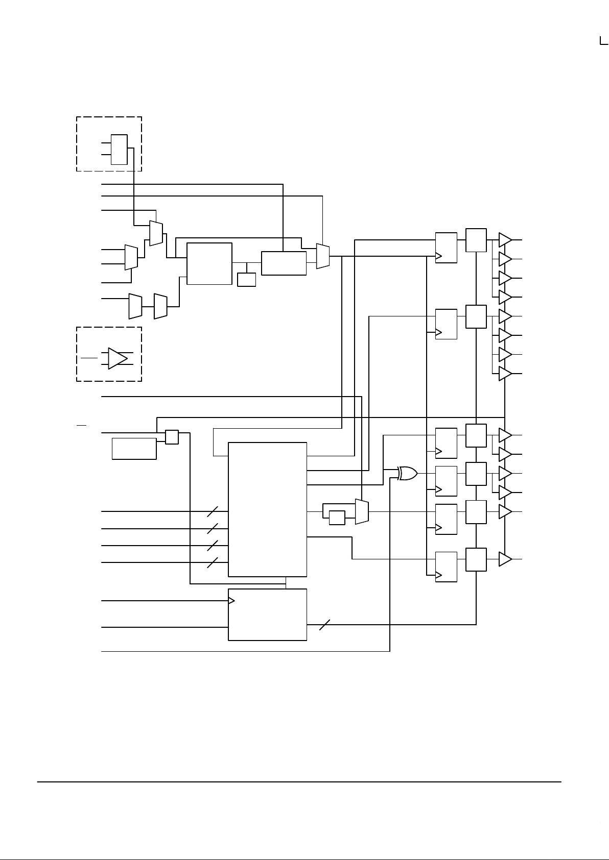
Figure 2. Logic Diagram
POWER-ON
RESET
VCO
PHASE
DETECTOR
LPF
PLL_En
Qa0
VCO_Sel
Q
Qa1
TCLK0
REF_SEL
Ext_FB
0
1
D
Qa2
Qa3
Sync
Frz
Qb0
Q
Qb1
D
Qb2
Qb3
Sync
Frz
Qc0
Q
Qc1
D
Qc2
Qc3
Sync
Frz
QFB
QD
Sync
Frz
fsela0:1
fselb0:1
Frz_Data
fselc0:1
fselFB0:1
÷
4, ÷6, ÷8, ÷12
÷
4, ÷6, ÷8, ÷10
÷
2, ÷4, ÷6, ÷8
0
1
QSync
QD
Sync
Frz
÷
2
÷
4, ÷6, ÷8, ÷10
Sync Pulse
Data Generator
Output Disable
Circuitry
Frz_Clk
12
2
2
2
2
MR/OE
0
1
TCLK1
TCLK_Sel
QD
Sync
Frz
Inv_Clk
fselFB2
xtal2
xtal1
972 OPTION
PCLK
PCLK
973 OPTION
Page 4

MPC972 MPC973
MOTOROLA TIMING SOLUTIONS
BR1333 — Rev 6
4
Figure 3. Timing Diagrams
fVCO
1:1 Mode
Qa
Qc
Sync
2:1 Mode
Qc(÷2)
Qa(÷6)
Sync
3:1 Mode
Qa
Qc
Sync
Qa(÷4)
Qc(
÷
6)
Sync
3:2 Mode
Qc(÷2)
Qa(
÷
8)
Sync
4:1 Mode
Qa(÷6)
Qc(
÷
8)
Sync
4:3 Mode
Qa(÷12)
Qc(÷2)
Sync
6:1 Mode
Page 5
MPC972 MPC973
TIMING SOLUTIONS
BR1333 — Rev 6
5 MOTOROLA
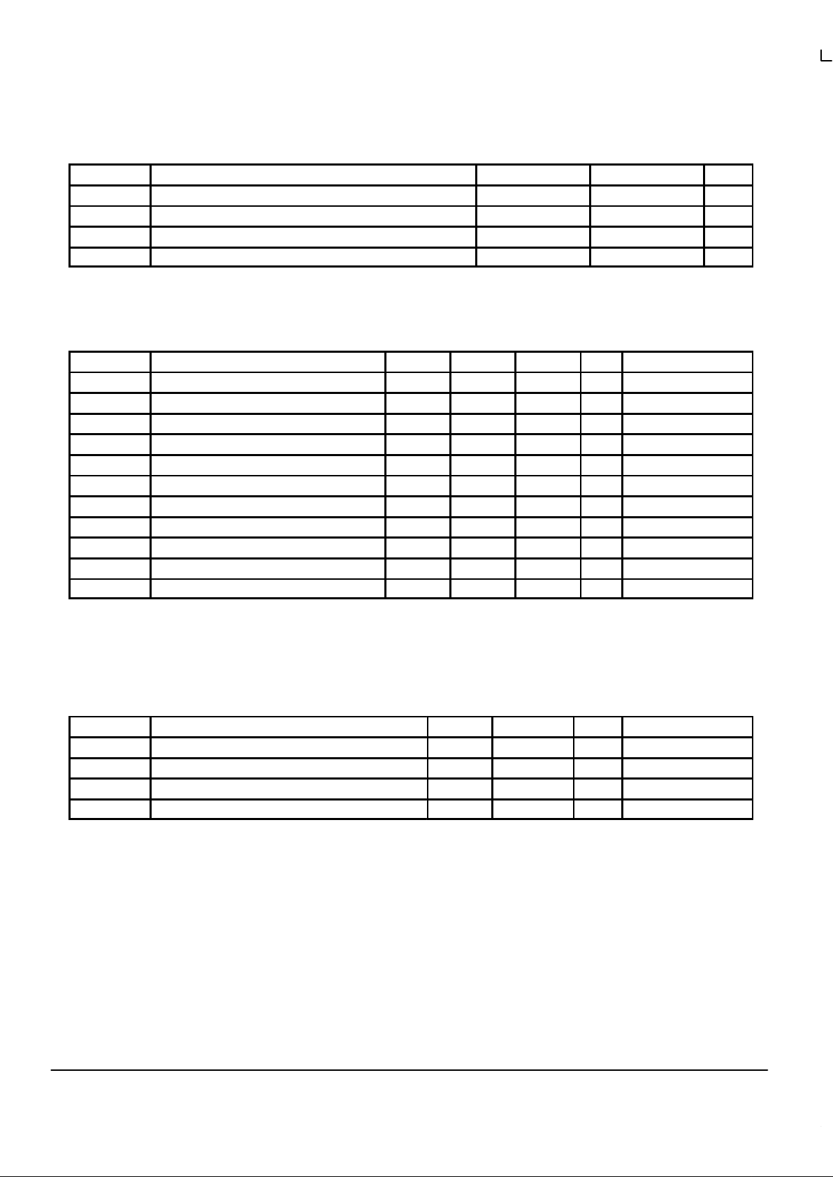
ABSOLUTE MAXIMUM RATINGS*
Symbol Parameter Min Max Unit
V
CC
Supply Voltage –0.3 4.6 V
V
I
Input Voltage –0.3 VDD + 0.3 V
I
IN
Input Current ±20 mA
T
Stor
Storage Temperature Range –40 125 °C
* Absolute maximum continuous ratings are those values beyond which damage to the device may occur. Exposure to these conditions or
conditions beyond those indicated may adversely affect device reliability. Functional operation under absolute-maximum-rated conditions is not
implied.
DC CHARACTERISTICS (Note 4.; TA = 10° to 70°C; VCC = 3.3V ±5%)
Symbol Characteristic Min Typ Max Unit Condition
V
IH
Input HIGH Voltage 2.0 3.6 V
V
IL
Input LOW Voltage 0.8 V
V
PP
Peak–to–Peak Input Voltage PECL_CLK 300 1000 mV
V
CMR
Common Mode Range PECL_CLK VCC–2.0 VCC–0.6 Note 1.
V
OH
Output HIGH Voltage 2.4 V IOH = –20mA (Note 2.)
V
OL
Output LOW Voltage 0.5 V IOL = 20mA (Note 2.)
I
IN
Input Current ±120 µA Note 3.
I
CC
Maximum Quiescent Supply Current 190 215 mA All VCC PIns
I
CCA
Analog VCC Current 15 20 mA
C
IN
Input Capacitance 4 pF
C
pd
Power Dissipation Capacitance 25 pF Per Output
1. V
CMR
is the difference from the most positive side of the differential input signal. Normal operation is obtained when the “High” input is within
the V
CMR
range and the input lies within the VPP specification.
2. The MPC972/973 outputs can drive series or parallel terminated 50Ω (or 50Ω to VCC/2) transmission lines on the incident edge (see Applications
Info section).
3. Inputs have pull–up/pull–down resistors which affect input current.
4. Special thermal handling may be required in some configurations.
PLL INPUT REFERENCE CHARACTERISTICS (TA = 10° to 70°C)
Symbol Characteristic Min Max Unit Condition
tr, t
f
TCLK Input Rise/Falls 3.0 ns
f
ref
Reference Input Frequency Note 5. 100, Note 5. MHz Note 5.
f
refDC
Reference Input Duty Cycle 25 75 %
t
xtal
Crystal Oscillator Frequency 10 25 MHz Note 6.
5. Maximum input reference frequency is limited by the VCO lock range and the feedback divider or 100MHz, minimum input reference frequency
is limited by the VCO lock range and the feedback divider.
6. See Applications Info section for more crystal information.
Page 6
MPC972 MPC973
MOTOROLA TIMING SOLUTIONS
BR1333 — Rev 6
6
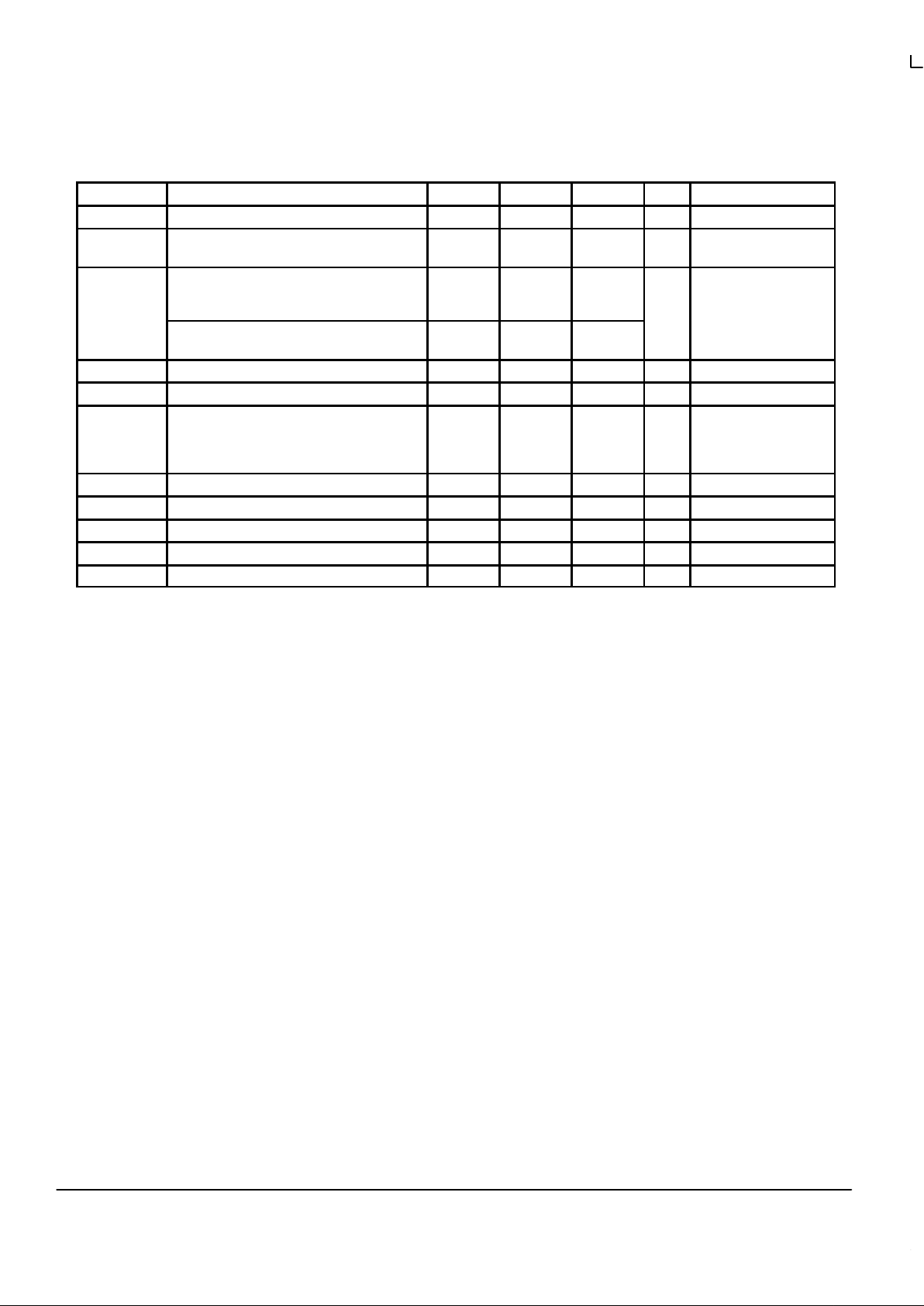
AC CHARACTERISTICS (TA = 10° to 70°C; VCC = 3.3V ±5%)
Symbol Characteristic Min Typ Max Unit Condition
tr, t
f
Output Rise/Fall Time (Note 7.) 0.15 1.2 ns 0.8 to 2.0V
t
pw
Output Duty Cycle (Note 7.) t
CYCLE
/2
–750
t
CYCLE
/2
±500
t
CYCLE
/2
+750
ps
t
pd
SYNC to Feedback MPC973 TCLK0
Propagation Delay TCLK1
PECL_CLK
–70
–130
–225
130
70
–25
330
270
175
ps Notes 7., 8.; QFB = ÷8
MPC972 TCLK0
TCLK1
–270
–330
130
70
530
470
t
os
Output-to-Output Skew 550 ps Note 7.
f
VCO
VCO Lock Range 200 480 MHz
f
max
Maximum Output Frequency Q (÷2)
Q (÷4)
Q (÷6)
Q (÷8)
125
120
80
60
MHz
t
jitter
Cycle–to–Cycle Jitter (Peak–to–Peak) ±100 ps
t
PLZ
, t
PHZ
Output Disable Time 2 8 ns
t
PZL
, t
PZH
Output ENable TIme 2 10 ns
t
lock
Maximum PLL Lock Time 10 ms
f
MAX
Maximum Frz_Clk Frequency 20 MHz
7. 50Ω transmission line terminated into VCC/2.
8. tpd is specified for a 50MHz input reference. The window will shrink/grow proportionally from the minimum limit with shorter/longer input
reference periods. The tpd does not include jitter.
APPLICATIONS INFORMATION
Programming the MPC972/973
The MPC972/973 is the most flexible frequency
programming device in the Motorola timing solution portfolio.
With three independent banks of four outputs as well as an
independent PLL feedback output the total number of
possible configurations is too numerous to tabulate. Table 1
tabulates the various selection possibilities for the three
banks of outputs. The divide numbers presented in the table
represent the divider applied to the output of the VCO for that
bank of outputs. To determine the relationship between the
three backs the three divide ratios would be compared. For
instance if a frequency relationship of 5:3:2 was desired the
following selection could be made. The Qb outputs could be
set to ÷10, the Qa outputs to ÷6 and the Qc outputs to ÷4.
With this output divide selection the desired 5:3:2 relationship
would be generated. For situations where the VCO will run at
relatively low frequencies the PLL may not be stable for the
desired divide ratios. For these circumstances the VCO_Sel
pin allows for an extra ÷2 to be added into the clock path.
When asserted this pin will maintain the desired output
relationships, but will provide an enhanced lock range for the
PLL. Once the output frequency relationship is set and the
VCO is in its stable range the feedback output would be
programmed to match the input reference frequency.
The MPC972/973 offers only an external feedback to the
PLL. A separate feedback output is provided to optimize the
flexibility of the device. If in the example above the input
reference frequency was equal to the lowest output
frequency the feedback output would be set in the ÷10 mode.
If the input needed to be half the lowest frequency output the
fselFB2 input could be asserted to half the feedback
frequency. This action multiplies the output frequencies by
two relative to the input reference frequency. With 7 unique
feedback divide capabilities there is a tremendous amount of
flexibility. Again assume the above 5:3:2 relationship is
needed with the highest frequency output equal to 100MHz. If
one was also constrained because the only reference
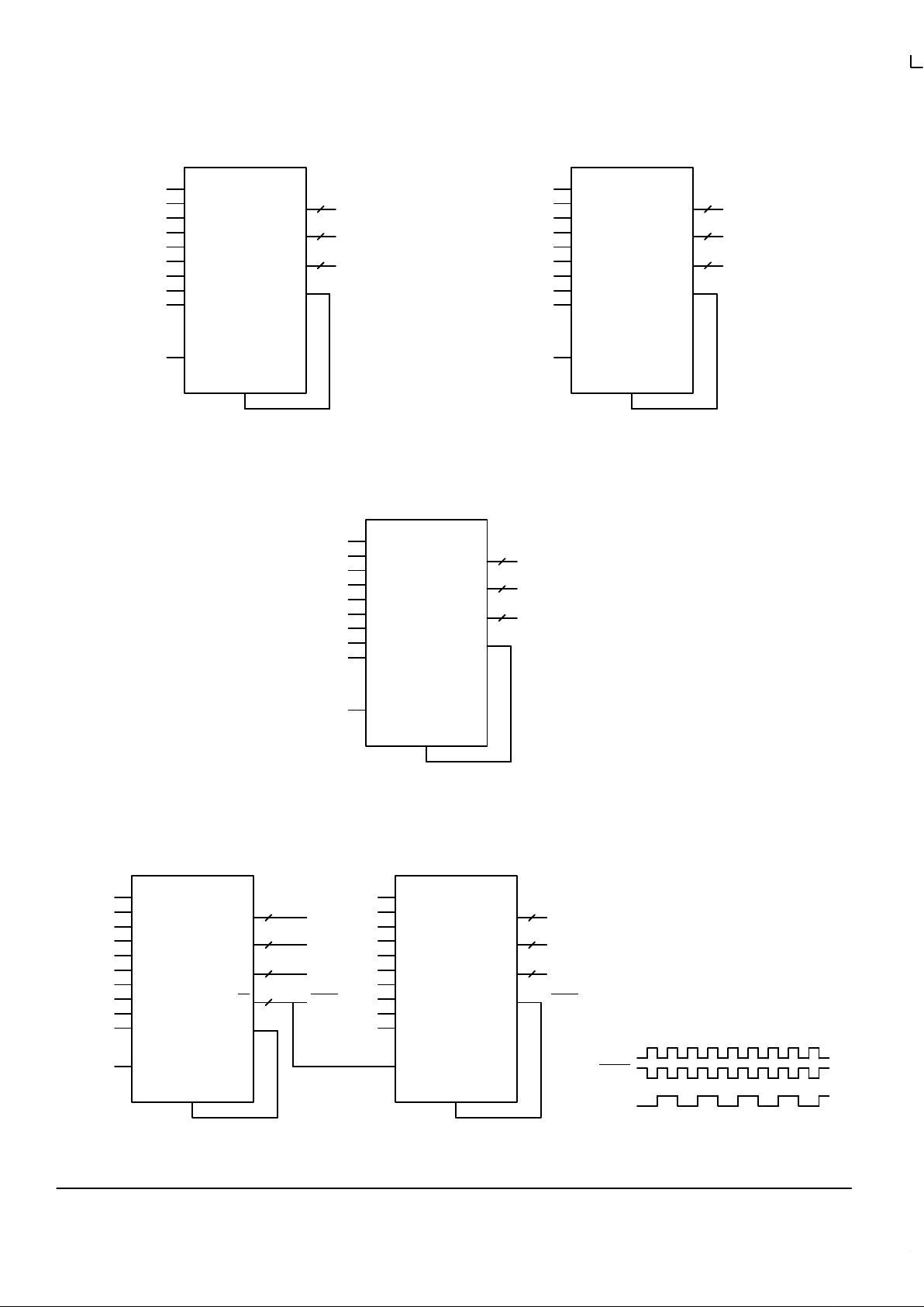
frequency available was 50MHz the setup in Figure 8 could
be used. The MPC972/973 provides the 100, 66 and 40MHz
outputs all synthesized from the 50MHz source. With its
multitude of divide ratio capabilities the MPC972/973 can
generate almost any frequency from a standard, common
frequency already present in a design. Figure 9 and
Figure 10 illustrate a few more examples of possible
MPC972/973 configurations.
The MPC972/973 has one more programming feature
added to its arsenal. The Inv_Clk input pin when asserted will
invert the Qc2 and Qc3 outputs. This inversion will not affect
the output–output skew of the device. This inversion allows
for the development of 180° phase shifted clocks. This output
could also be used as a feedback output to the MPC972/973
or a second PLL device to generate early or late clocks for a
specific design. Figure 11 illustrates the use of two
Page 7
MPC972 MPC973
TIMING SOLUTIONS
BR1333 — Rev 6
7 MOTOROLA
MPC972/973’s to generate two banks of clocks with one
bank divided by 2 and delayed by 180° relative to the first.
Using the MPC973 as a Zero Delay Buffer
The external feedback of the MPC973 clock driver allows
for its use as a zero delay buffer . By using one of the outputs
as a feedback to the PLL the propagation delay through the
device is eliminated. The PLL works to align the output edge
with the input reference edge thus producing a near zero
delay . The reference frequency affects the static phase offset
of the PLL and thus the relative delay between the inputs and
outputs. Because the static phase offset is a function of the
reference clock the Tpd of the MPC973 is a function of the
configuration used.
When used as a zero delay buffer the MPC973 will likely
be in a nested clock tree application. For these applications
the MPC973 offers a L VPECL clock input as a PLL reference.
This allows the user to use LVPECL as the primary clock
distribution device to take advantage of its far superior skew
performance. The MPC973 then can lock onto the LVPECL
reference and translate with near zero delay to low skew
LVCMOS outputs. Clock trees implemented in this fashion
will show significantly tighter skews than trees developed
from CMOS fanout buffers.
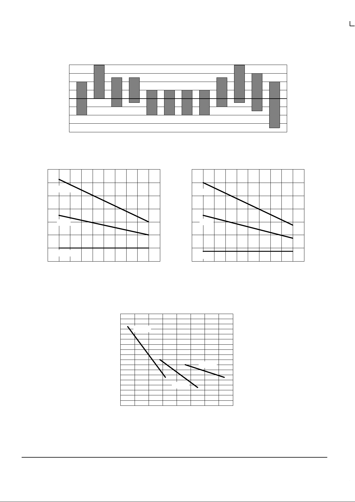
To calculate the overall uncertainty between the input
reference clock and the output clocks the following approach
should be used. Figure 4 through Figure 7 contain the
performance information required to calculate the overall
uncertainty . Since the overall skew performance is a function
of the input reference frequency all of the graphs provide
relavent data with respect to the input reference frequency.
The overall uncertainty can be broken down into three
parts; the static phase offset variation (Tpd), the I/O phase
jitter and the output skew. If we assume that we have a
75MHz reference clock, from the graphs we can pull the
following information for static phase offset (SPO) and I/O
jitter: the SPO variation will be 300ps (–100ps to +200ps
assuming a TCLK is used) and the I/O jitter will be ±105ps
(assuming a VCO/6 configuration and a ±3 sigma for min and
max). The nominal delay from Figure 5 is 50ps so that the
propagation delay between the reference clock and the
feedback clock is 50ps ±255ps.
Figure 4 can now be used to establish the uncertainty
between the reference clock and all of the outputs for the
MPC973. Figure 4 provides the skew of the MC973 outputs
with respect to the feedback output. From Figure 4, if all of
the outputs are used the propagation delay of the device will
range from –555ps (50ps – 255ps – 350ps) to +705ps (50ps
+ 255ps + 400ps) for a total uncertainty of 1.26ns. This
1.26ns uncertainty would hold true if multiple 973’s are used
in parallel in the application given that the skew between the
reference clock for the devices were zero. Notice from the
data in Figure 4 that if a subset of the outputs were used
significant reductions in uncertainty could be obtained.
SYNC Output Description
In situations where output frequency relationships are not
integer multiples of each other there is a need for a signal for
system synchronization purposes. The SYNC output of the
MPC972/973 is designed to specifically address this need.
The MPC972/973 monitors the relationship between the Qa
and the Qc banks of outputs. It provides a low going pulse,
one period in duration, one period prior to the coincident
rising edges of the Qa and Qc outputs. The duration and the
placement of the pulse is dependent on the higher of the Qa
and Qc output frequencies. The timing diagrams in the data
sheet show the various waveforms for the SYNC output.
Note that the SYNC output is defined for all possible
combinations of the Qa and Qc outputs even though under
some relationships the lower frequency clock could be used
as a synchronizing signal.
Table 1. Programmable Output Frequency Relationships (VCO_Sel=‘1’)
fsela1 fsela0 Qa fselb1 fselb0 Qb fselc1 fselc0 Qc
0
0
1
1
0
1
0
1
VCO/4
VCO/6
VCO/8
VCO/12
0
0
1
1
0
1
0
1
VCO/4
VCO/6
VCO/8
VCO/10
0
0
1
1
0
1
0
1
VCO/2
VCO/4
VCO/6
VCO/8
Table 2. Programmable Output Frequency Relationships (VCO_Sel=‘1’)
fselFB2 fselFB1 fselFB0 QFB
0
0
0
0
0
0
1
1
0
1
0
1
VCO/4
VCO/6
VCO/8
VCO/10
1
1
1
1
0
0
1
1
0
1
0
1
VCO/8
VCO/12
VCO/16
VCO/20
Page 8
MPC972 MPC973
MOTOROLA TIMING SOLUTIONS
BR1333 — Rev 6
8
Figure 4. Skews Relative to QFB
–400
–300
–200
–100
0
100
200
300
400
Qc3 Qc2 Qc1 Qc0 Qb3 Qb2 Qb1 Qb0 Qa3 Qa2 Qa1 Qa0
ps
–200
–100
0
100
200
300
400
500
10 20 30 40 50 60 70 80 90 100 110
Tpd (ps)
Figure 5.
Static Phase Offset versus Reference Frequency
Tpd versus TCLK
Reference Clock Frequency (MHz)
Min
Nom
Max
–300
–200
–100
0
100
200
300
400
10 20 30 40 50 60 70 80 90 100 110
Tpd (ps)
Figure 6.
Static Phase Offset versus Reference Frequency
Tpd versus PECL_CLK
Reference Clock Frequency (MHz)
Min
Nom
Max
24
26
28
30
32
34
36
38
40
42
44
46
48
50
52
54
56
58
60
30 40 50 60 70 80 90 100 110
I/O Jitter (ps)
Figure 7.
Phase Jitter versus Reference Frequency
I/O Jitter
Reference Clock Frequency (MHz)
VCO/4
VCO/6
VCO/8
1σ
Page 9
MPC972 MPC973
TIMING SOLUTIONS
BR1333 — Rev 6
9 MOTOROLA
‘0’
MPC972
Figure 8. Programming Configuration Example
fsela0‘0’
fsela1
fselb0
fselb1
Input Ref50MHz
fselc0
fselc1
fselFB0
fselFB1
fselFB2
VCO = 400MHz
Ext_FB
100MHzQa
40MHzQb
66.66MHzQc
4
4
4
50MHzQFB
‘1’
‘1’
‘0’
‘1’
‘0’
‘1’
‘0’
‘0’
MPC972
Figure 9. Generating Pentium Clocks from Floppy Clock
fsela0‘0’
fsela1
fselb0
fselb1
Input Ref24MHz
fselc0
fselc1
fselFB0
fselFB1
fselFB2
Ext_FB
60MHz (Processor)Qa
60MHz (Processor)Qb
30MHz (PCI)Qc
4
4
4
24MHz (Floppy Disk Clk)QFB
‘0’
‘0’
‘1’
‘1’
‘1’
‘1’
‘0’
‘1’
MPC972
Figure 10. Generating MPC604 Clocks from Ethernet Clocks
fsela0‘1’
fsela1
fselb0
fselb1
Input Ref20MHz
fselc0
fselc1
fselFB0
fselFB1
fselFB2
Ext_FB
33MHz (PCI)Qa
50MHz (Processor)Qb
50MHz (Processor)Qc
4
4
4
20MHz (Ethernet)QFB
‘0’
‘1’
‘1’
‘1’
‘1’
‘1’
‘1’
Figure 11. Phase Delay Using Multiple MPC972/973’s
‘0’
MPC972/973
fsela0‘0’
fsela1
fselb0
fselb1
Input Ref66MHz
fselc0
fselc1
fselFB0
fselFB1
fselFB2
Ext_FB
66MHzQa
66MHzQb
66MHzQc
4
4
2
QFB
‘0’
‘0’
‘0’
‘1’
‘0’
‘1’
‘0’
‘1’
MPC972/973
fsela0‘0’
fsela1
fselb0
fselb1
Input Ref
fselc0
fselc1
fselFB0
fselFB1
fselFB2
Ext_FB
33MHz Shifted 90
°
Qa
33MHz Shifted 90
°
Qb
33MHz Shifted 90
°
Qc
4
4
4
66MHzQFB
‘0’
‘1’
‘1’
‘1’
‘0’
‘0’
‘0’
Inv_Clk‘1’ Inv_Clk‘0’
66MHzQc
2
66MHz
33MHz
Shifted 90
°
66MHz
Page 10
MPC972 MPC973
MOTOROLA TIMING SOLUTIONS
BR1333 — Rev 6
10
Using the On–Board Crystal Oscillator
The MPC972 features an on–board crystal oscillator to
allow for seed clock generation as well as final distribution.
The on–board oscillator is completely self contained so that
the only external component required is the crystal. As the
oscillator is somewhat sensitive to loading on its inputs the
user is advised to mount the crystal as close to the MPC972
as possible to avoid any board level parasitics. To facilitate
co–location surface mount crystals are recommended, but
not required.
The oscillator circuit is a series resonant circuit as
opposed to the more common parallel resonant circuit, this
eliminates the need for large on–board capacitors. Because
the design is a series resonant design for the optimum
frequency accuracy a series resonant crystal should be used
(see specification table below). Unfortunately most of the
shelf crystals are characterized in a parallel resonant mode.
However a parallel resonant crystal is physically no different
than a series resonant crystal, a parallel resonant crystal is
simply a crystal which has been characterized in its parallel
resonant mode. Therefore in the majority of cases a parallel
specified crystal can be used with the MPC972 with just a
minor frequency error due to the actual series resonant
frequency of the parallel resonant specified crystal. Typically
a parallel specified crystal used in a series resonant mode
will exhibit an oscillatory frequency a few hundred ppm lower
than the specified value. For most processor
implementations a few hundred ppm translates into kHz
inaccuracies, a level which does not represent a major issue.
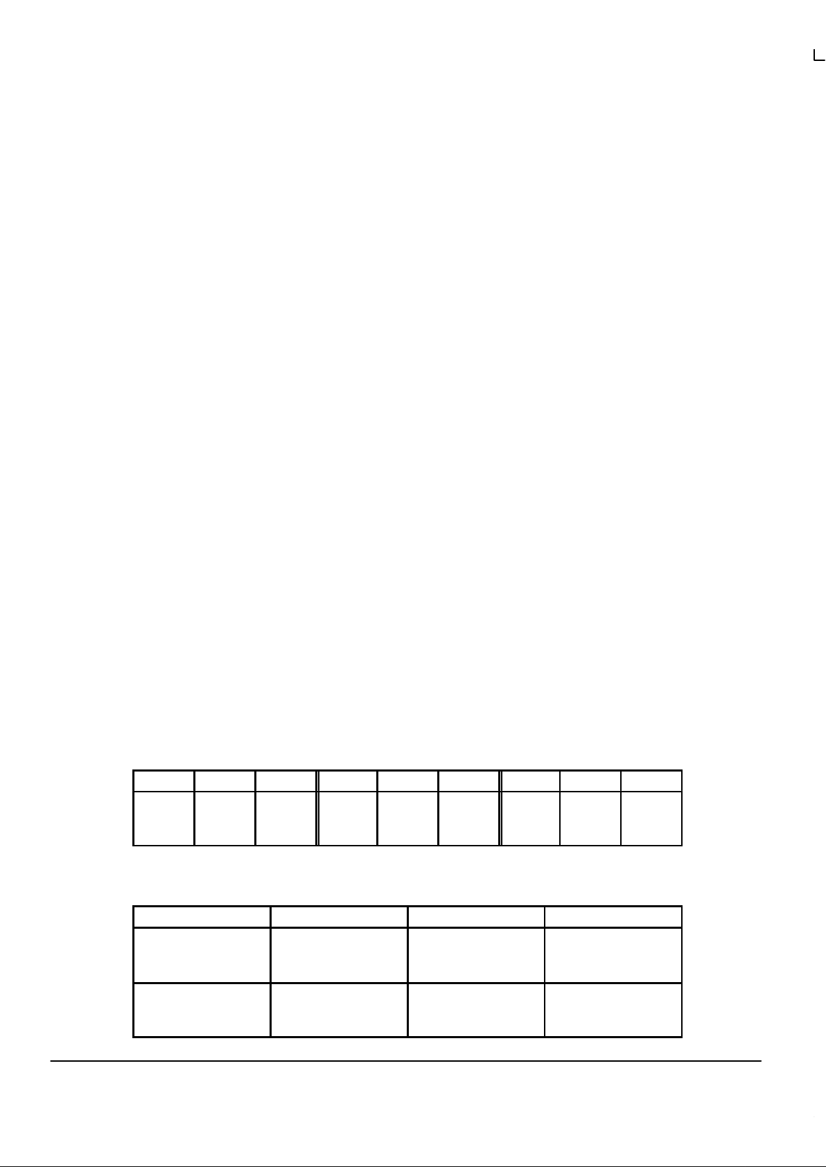
Table 3. Crystal Specifications
Parameter Value
Crystal Cut Fundamental AT Cut
Resonance Series Resonance*
Frequency Tolerance ±75ppm at 25°C
Frequency/Temperature Stability ±150pm 0 to 70°C
Operating Range 0 to 70°C
Shunt Capacitance 5–7pF
Equivalent Series Resistance (ESR) 50 to 80Ω Max
Correlation Drive Level 100µW
Aging 5ppm/Yr (First 3 Y ears)
* See accompanying text for series versus parallel resonant
discussion.
The MPC972/973 is a clock driver which was designed to
generate outputs with programmable frequency relationships
and not a synthesizer with a fixed input frequency. As a result
the crystal input frequency is a function of the desired output
frequency. For a design which utilizes the external feedback
to the PLL the selection of the crystal frequency is straight
forward; simply chose a crystal which is equal in frequency to
the fed back signal.
Power Supply Filtering
The MPC972/973 is a mixed analog/digital product and
exhibits some sensitivities that would not necessarily be seen
on a fully digital product. Analog circuitry is naturally
susceptible to random noise, especially if this noise is seen
on the power supply pins. The MPC972/973 provides
separate power supplies for the output buffers (V
CCO
) and
the internal PLL (VCCA) of the device. The purpose of this
design technique is to try and isolate the high switching noise
digital outputs from the relatively sensitive internal analog
phase–locked loop. In a controlled environment such as an
evaluation board this level of isolation is sufficient. However,
in a digital system environment where it is more difficult to
minimize noise on the power supplies a second level of
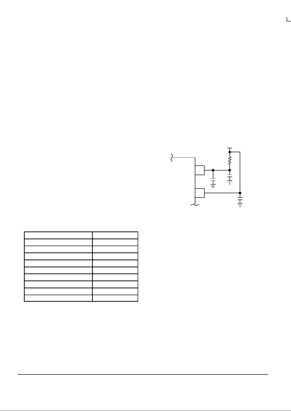
isolation may be required. The simplest form of isolation is a
power supply filter on the VCCA pin for the MPC972/973.
Figure 12. Power Supply Filter
VCCA
VCC
MPC972/973
0.01µF
22
µ
F
0.01
µ
F
3.3V
RS=5–10
Ω
Figure 12 illustrates a typical power supply filter scheme.
The MPC972/973 is most susceptible to noise with spectral
content in the 1KHz to 1MHz range. Therefore the filter
should be designed to target this range. The key parameter
that needs to be met in the final filter design is the DC voltage
drop that will be seen between the VCC supply and the VCCA
pin of the MPC972/973. From the data sheet the I
VCCA
current (the current sourced through the VCCA pin) is
typically 15mA (20mA maximum), assuming that a minimum
of 3.0V must be maintained on the VCCA pin very little DC
voltage drop can be tolerated when a 3.3V VCC supply is
used. The resistor shown in Figure 12 must have a
resistance of 5–10Ω to meet the voltage drop criteria. The RC
filter pictured will provide a broadband filter with
approximately 100:1 attenuation for noise whose spectral
content is above 20KHz. As the noise frequency crosses the
series resonant point of an individual capacitor it’s overall
impedance begins to look inductive and thus increases with
increasing frequency. The parallel capacitor combination
shown ensures that a low impedance path to ground exists
for frequencies well above the bandwidth of the PLL.
Although the MPC972/973 has several design features to
minimize the susceptibility to power supply noise (isolated
power and grounds and fully differential PLL) there still may
be applications in which overall performance is being
degraded due to system power supply noise. The power
supply filter schemes discussed in this section should be
Page 11
MPC972 MPC973
TIMING SOLUTIONS
BR1333 — Rev 6
11 MOTOROLA
adequate to eliminate power supply noise related problems
in most designs.
Driving Transmission Lines
The MPC972/973 clock driver was designed to drive high
speed signals in a terminated transmission line environment.
To provide the optimum flexibility to the user the output
drivers were designed to exhibit the lowest impedance
possible. With an output impedance of less than 10Ω the
drivers can drive either parallel or series terminated
transmission lines. For more information on transmission
lines the reader is referred to application note AN1091 in the
Timing Solutions brochure (BR1333/D).
In most high performance clock networks point–to–point
distribution of signals is the method of choice. In a
point–to–point scheme either series terminated or parallel
terminated transmission lines can be used. The parallel
technique terminates the signal at the end of the line with a
50Ω resistance to VCC/2. This technique draws a fairly high
level of DC current and thus only a single terminated line can
be driven by each output of the MPC972/973 clock driver. For
the series terminated case however there is no DC current
draw, thus the outputs can drive multiple series terminated
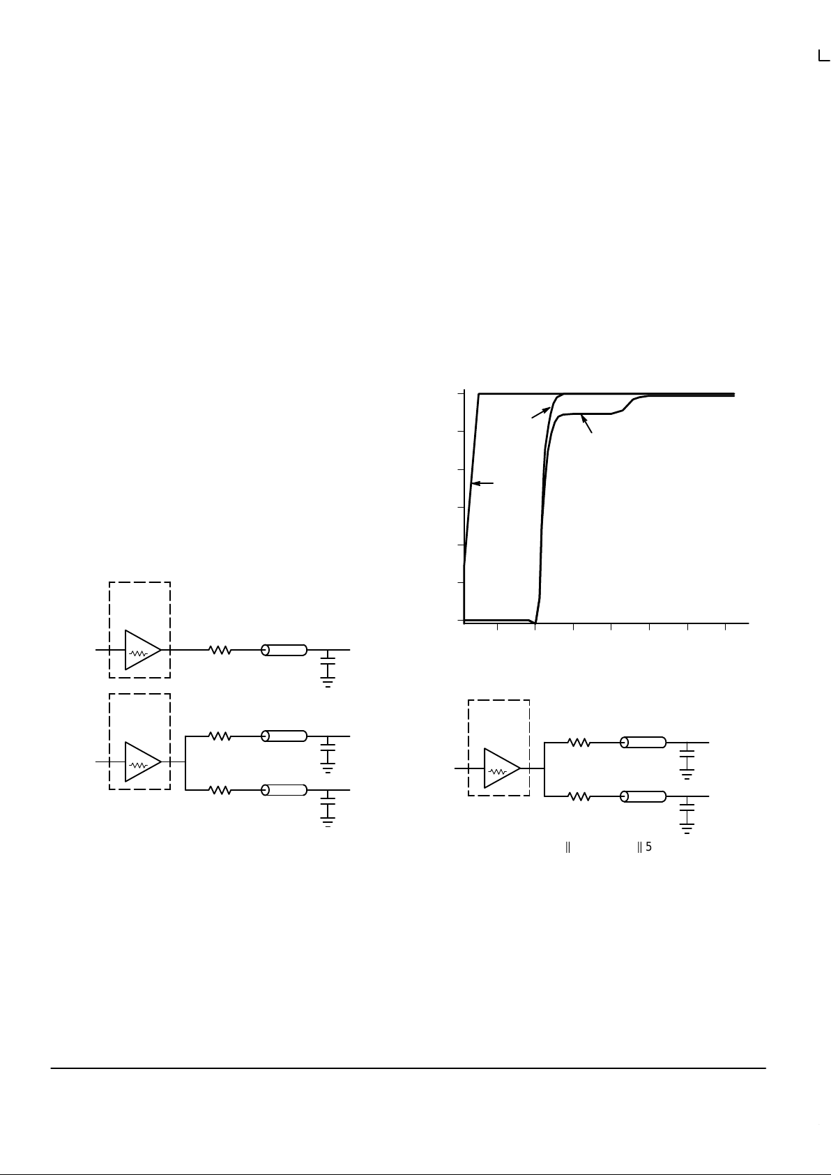
lines. Figure 13 illustrates an output driving a single series
terminated line vs two series terminated lines in parallel.
When taken to its extreme the fanout of the MPC972/973
clock driver is effectively doubled due to its capability to drive
multiple lines.
Figure 13. Single versus Dual Transmission Lines
7
Ω
IN
MPC972/973
OUTPUT
BUFFER
RS = 43
Ω
ZO = 50
Ω
OutA
7
Ω
IN
MPC972/973
OUTPUT
BUFFER
RS = 43
Ω
ZO = 50
Ω
OutB0
RS = 43
Ω
ZO = 50
Ω
OutB1
The waveform plots of Figure 14 show the simulation
results of an output driving a single line vs two lines. In both
cases the drive capability of the MPC972/973 output buffers
is more than sufficient to drive 50Ω transmission lines on the
incident edge. Note from the delay measurements in the
simulations a delta of only 43ps exists between the two
differently loaded outputs. This suggests that the dual line
driving need not be used exclusively to maintain the tight
output–to–output skew of the MPC972/973. The output
waveform in Figure 14 shows a step in the waveform, this
step is caused by the impedance mismatch seen looking into
the driver. The parallel combination of the 43Ω series resistor
plus the output impedance does not match the parallel
combination of the line impedances. The voltage wave
launched down the two lines will equal:
VL = VS ( Zo / Rs + Ro +Zo) = 3.0 (25/53.5) = 1.40V
At the load end the voltage will double, due to the near
unity reflection coefficient, to 2.8V. It will then increment
towards the quiescent 3.0V in steps separated by one round
trip delay (in this case 4.0ns).
Since this step is well above the threshold region it will not
cause any false clock triggering, however designers may be
uncomfortable with unwanted reflections on the line. To
better match the impedances when driving multiple lines the
situation in Figure 15 should be used. In this case the series
terminating resistors are reduced such that when the parallel
combination is added to the output buffer impedance the line
impedance is perfectly matched.
Figure 14. Single versus Dual Waveforms
TIME (nS)
VOLTAGE (V)
3.0
2.5
2.0
1.5
1.0
0.5
0
2 4 6 8 10 12 14
OutB
tD = 3.9386
OutA
tD = 3.8956
In
Figure 15. Optimized Dual Line Termination
7
Ω
MPC972/973
OUTPUT
BUFFER
RS = 36
Ω
ZO = 50
Ω
RS = 36
Ω
ZO = 50
Ω
7Ω + 36Ω k 36Ω = 50Ω k 50Ω
25Ω = 25Ω
SPICE level output buffer models are available for
engineers who want to simulate their specific interconnect
schemes. In addition IV characteristics are in the process of
being generated to support the other board level simulators in
general use.
Using the Output Freeze Circuitry
With the recent advent of a “green” classification for
computers the desire for unique power management among
system designers is keen. The individual output enable
Page 12
MPC972 MPC973
MOTOROLA TIMING SOLUTIONS
BR1333 — Rev 6
12
control of the MPC972/973 allows designers, under software
control, to implement unique power management schemes
into their designs. Although useful, individual output control
at the expense of one pin per output is too high, therefore a
simple serial interface was derived to economize on the
control pins.
The freeze control logic provides a mechanism through
which the MPC972 clock outputs may be frozen (stopped in
the logic ‘0’ state):
The freeze mechanism allows serial loading of the 12–bit
Serial Input Register, this register contains one program–
mable freeze enable bit for 12 of the 14 output clocks. The
Qc0 and QFB outputs cannot be frozen with the serial port,
this avoids any potential lock up situation should an error
occur in the loading of the Serial Input Register. The user
may programmably freeze an output clock by writing logic ‘0’
to the respective freeze enable bit. Likewise, the user may
programmably unfreeze an output clock by writing logic ‘1’ to
the respective enable bit.
The freeze logic will never force a newly–frozen clock to a
logic ‘0’ state before the time at which it would normally
transition there. The logic simply keeps the frozen clock at
logic ‘0’ once it is there. Likewise, the freeze logic will never
force a newly–unfrozen clock to a logic ‘1’ state before the
time at which it would normally transition there. The logic
re–enables the unfrozen clock during the time when the
respective clock would normally be in a logic ‘0’ state,
eliminating the possibility of ‘runt’ clock pulses.
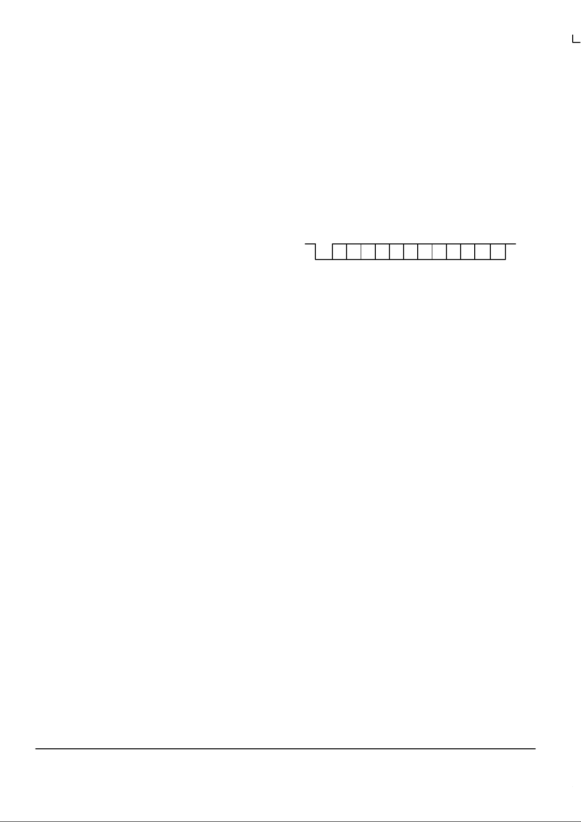
The user may write to the Serial Input register through the
Frz_Data input by supplying a logic ‘0’ start bit followed
serially by 12 NRZ freeze enable bits. The period of each
Frz_Data bit equals the period of the free–running Frz_Clk
signal. The Frz_Data serial transmission should be timed so
the MPC972 can sample each Frz_Data bit with the rising
edge of the free–running Frz_Clk signal.
Figure 16. Freeze Data Input Protocol
D1 D2 D3 D4 D5 D6 D7 D8 D9 D10 D11D0
Start
Bit
D0–D3 are the control bits for Qa0–Qa3, respectively
D4–D7 are the control bits for Qb0–Qb3, respectively
D8–D10 are the control bits for Qc1–Qc3, respectively
D11 is the control bit for QSync
Page 13
MPC972 MPC973
TIMING SOLUTIONS
BR1333 — Rev 6
13 MOTOROLA
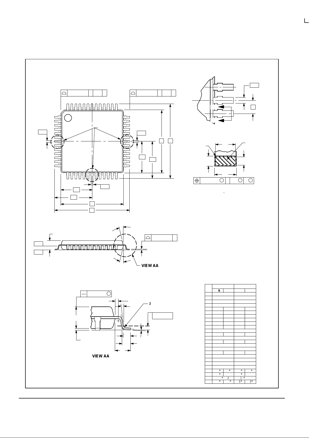
OUTLINE DIMENSIONS
FA SUFFIX
TQFP PACKAGE
CASE 848D–03
ISSUE C
F
NOTES:
1. DIMENSIONING AND TOLERANCING PER ANSI
Y14.5M, 1982.
2. CONTROLLING DIMENSION: MILLIMETER.
3. DATUM PLANE –H– IS LOCATED AT BOTTOM OF
LEAD AND IS COINCIDENT WITH THE LEAD
WHERE THE LEAD EXITS THE PLASTIC BODY AT
THE BOTTOM OF THE PARTING LINE.
4. DATUMS –L–, –M– AND –N– TO BE DETERMINED
AT DATUM PLANE –H–.
5. DIMENSIONS S AND V TO BE DETERMINED AT
SEATING PLANE –T–.
6. DIMENSIONS A AND B DO NOT INCLUDE MOLD
PROTRUSION. ALLOWABLE PROTRUSION IS
0.25 (0.010) PER SIDE. DIMENSIONS A AND B DO
INCLUDE MOLD MISMATCH AND ARE
DETERMINED AT DATUM PLANE -H-.
7. DIMENSION D DOES NOT INCLUDE DAMBAR
PROTRUSION. DAMBAR PROTRUSION SHALL
NOT CAUSE THE LEAD WIDTH TO EXCEED 0.46
(0.018). MINIMUM SPACE BETWEEN
PROTRUSION AND ADJACENT LEAD OR
PROTRUSION 0.07 (0.003).
VIEW AA
VIEW AA
2 X R R1
AB
AB
VIEW Y
SECTION AB–AB
ROTATED 90_ CLOCKWISE
DIMAMIN MAX MIN MAX
INCHES
10.00 BSC 0.394 BSC
MILLIMETERS
A1 5.00 BSC 0.197 BSC
B 10.00 BSC 0.394 BSC
B1 5.00 BSC 0.197 BSC
C ––– 1.70 ––– 0.067
C1 0.05 0.20 0.002 0.008
C2 1.30 1.50 0.051 0.059
D 0.20 0.40 0.008 0.016
E 0.45 0.030
F 0.22 0.35 0.009 0.014
G 0.65 BSC
0.75 0.018
0.026 BSC
J 0.07 0.20 0.003 0.008
K 0.50 REF 0.020 REF
R1 0.08 0.20 0.003 0.008
S 12.00 BSC 0.472 BSC
S1 6.00 BSC 0.236 BSC
U 0.09 0.16 0.004 0.006
V 12.00 BSC 0.472 BSC
V1 6.00 BSC 0.236 BSC
W 0.20 REF 0.008 REF
Z 1.00 REF 0.039 REF
C
L
–X–
X=L, M, N
1
13
14
26
27
39
4052
4X TIPS
4X
N0.20 (0.008) H L–M N0.20 (0.008) T L–M
3X VIEW Y
SEATING
PLANE
C
0.10 (0.004) T
4X θ3
4X θ2
S
0.05 (0.002)
0.25 (0.010)
GAGE PLANE
C2
C1
W
K
E
Z
S
L–M
M
0.13 (0.005) N
S
T
PLATING
BASE METAL
D
J
U
B V
B1
A
S
V1
A1
S1
–L–
–N–
–M–
–H–
–T–
θ1
θ
G
θ
1
θ
θ
3
θ
2
07
__
12
513
_
_
_
07
__
0
_
0
_
––– –––
REF
12
_
REF
13
_
5
_
Page 14

MPC972 MPC973
MOTOROLA TIMING SOLUTIONS
BR1333 — Rev 6
14
Motorola reserves the right to make changes without further notice to any products herein. Motorola makes no warranty , representation or guarantee regarding
the suitability of its products for any particular purpose, nor does Motorola assume any liability arising out of the application or use of any product or circuit, and
specifically disclaims any and all liability, including without limitation consequential or incidental damages. “T ypical” parameters which may be provided in Motorola
data sheets and/or specifications can and do vary in different applications and actual performance may vary over time. All operating parameters, including “Typicals”
must be validated for each customer application by customer’s technical experts. Motorola does not convey any license under its patent rights nor the rights of
others. Motorola products are not designed, intended, or authorized for use as components in systems intended for surgical implant into the body, or other
applications intended to support or sustain life, or for any other application in which the failure of the Motorola product could create a situation where personal injury
or death may occur. Should Buyer purchase or use Motorola products for any such unintended or unauthorized application, Buyer shall indemnify and hold Motorola
and its officers, employees, subsidiaries, affiliates, and distributors harmless against all claims, costs, damages, and expenses, and reasonable attorney fees
arising out of, directly or indirectly, any claim of personal injury or death associated with such unintended or unauthorized use, even if such claim alleges that
Motorola was negligent regarding the design or manufacture of the part. Motorola and are registered trademarks of Motorola, Inc. Motorola, Inc. is an Equal
Opportunity/Affirmative Action Employer.
MPC972/D
◊
Mfax is a trademark of Motorola, Inc.
How to reach us:
USA/EUROPE/Locations Not Listed: Motorola Literature Distribution; JAPAN: Nippon Motorola Ltd.: SPD, Strategic Planning Office, 4–32–1,
P.O. Box 5405, Denver, Colorado 80217. 1–303–675–2140 or 1–800–441–2447 Nishi–Gotanda, Shinagawa–ku, Tokyo 141, Japan. 81–3–5487–8488
Customer Focus Center: 1–800–521–6274
Mfax: [email protected] – TOUCHTONE 1–602–244–6609 ASIA/PACIFIC: Motorola Semiconductors H.K. Ltd.; 8B Tai Ping Industrial Park,
Moto rola Fax Back System – US & Canada ONLY 1–800–774–1848 51 Ting Kok Road, Tai Po, N.T ., Hong Kong. 852–26629298
– http://sps.motorola.com/mfax/
HOME PAGE: http://motorola.com/sps/
 Loading...