

Page 1
SEMICONDUCTOR TECHNICAL DATA
1
REV 3
Motorola, Inc. 1997
1/97
"
!
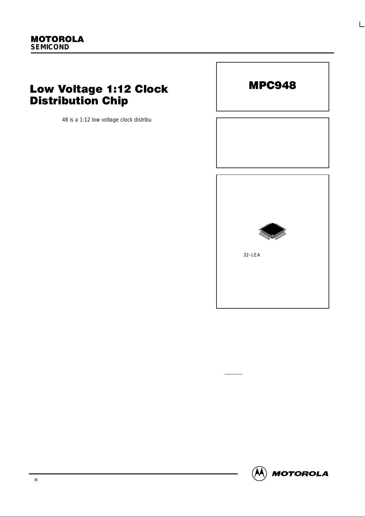
The MPC948 is a 1:12 low voltage clock distribution chip. The device
features the capability to select either a differential LVPECL or a LVTTL
compatible input. The 12 outputs are L VCMOS or LVTTL compatible and
feature the drive strength to drive 50Ω series terminated transmission
lines. With output–to–output skews of 350ps, the MPC948 is ideal as a
clock distribution chip for the most demanding of synchronous systems.
For a similar product targeted at a lower price/performance point, please
consult the MPC947 data sheet.
• Clock Distribution for PowerPC 620 L2 Cache
• L VPECL or LVCMOS/LVTTL Clock Input
• 350ps Maximum Output–to–Output Skew
• Drives Up to 24 Independent Clock Lines
• Maximum Output Frequency of 150MHz
• Synchronous Output Enable
• Tristatable Outputs
• 32–Lead TQFP Packaging
• 3.3V V
CC
Supply Voltage
With an output impedance of approximately 7Ω, in both the HIGH and
LOW logic states, the output buffers of the MPC948 are ideal for driving
series terminated transmission lines. More specifically, each of the 12
MPC948 outputs can drive two series terminated 50Ω transmission lines.
With this capability, the MPC948 has an effective fanout of 1:24 in
applications where each line drives a single load. With this level of fanout,
the MPC948 provides enough copies of low skew clocks for high
performance synchronous systems, including use as a clock distribution
chip for the L2 cache of a PowerPC 620 based system.
The differential LVPECL inputs of the MPC948 allow the device to interface directly with a LVPECL fanout buffer like the
MC100LVE111 to build very wide clock fanout trees or to couple to a high frequency clock source. The LVCMOS/LVTTL input
provides a more standard interface for applications requiring only a single clock distribution chip at relatively low frequencies. In
addition, the two clock sources can be used to provide for a test clock interface as well as the primary system clock. A logic HIGH
on the TTL_CLK_Sel pin will select the TTL level clock input.
All of the control inputs are LVCMOS/LVTTL compatible. The MPC948 provides a synchronous output enable control to allow
for starting and stopping of the output clocks. A logic high on the Sync_OE pin will enable all of the outputs. Because this control
is synchronized to the input clock, potential output glitching or runt pulse generation is eliminated. In addition, for board level test,
the outputs can be tristated via the tristate control pin. A logic LOW applied to the Tristate
input will force all of the outputs into
high impedance. Note that all of the MPC948 inputs have internal pullup resistors.
The MPC948 is fully 3.3V compatible. The 32–lead TQFP package was chosen to optimize performance, board space and
cost of the device. The 32–lead TQFP has a 7x7mm body size with a conservative 0.8mm pin spacing.
PowerPC is a trademark of International Business Machines Corporation.
LOW VOLTAGE
1:12 CLOCK
DISTRIBUTION CHIP
FA SUFFIX
32–LEAD TQFP PACKAGE
CASE 873A–02
Page 2

MPC948
MOTOROLA TIMING SOLUTIONS
BR1333 — Rev 6
2
Figure 1. Logic Diagram
Figure 2. 32–Lead Pinout (Top View)
FUNCTION TABLES
TTL_CLK_Sel Input
0
1
PECL_CLK
TTL_CLK
Sync_OE Outputs
0
1
Disabled
Enabled
Tristate Outputs
0
1
Tristate
Enabled
TTL_CLK
Sync_OE
Q
Figure 3. Sync_OE Timing Diagram
TTL_CLK
Q0–Q11
PECL_CLK
0
1
TTL_CLK_Sel
Sync_OE
Tristate
12
PECL_CLK
Q3
VCCO
Q2
GND
Q1
VCCO
Q0
GND
GND
Q8
VCCO
Q9
GND
Q10
VCCO
Q11
GND
Q4
VCCOQ5GND
Q6
VCCO
Q7
TTL_CLK_Sel
TTL_CLK
PECL_CLK
PECL_CLK
Sync_OE
Tristate
VCCI
GND
25
26
27
28
29
30
31
32
15
14
13
12
11
10
9
12345678
24 23 22 21 20 19 18 17
16
MPC948
Page 3
MPC948
TIMING SOLUTIONS
BR1333 — Rev 6
3 MOTOROLA
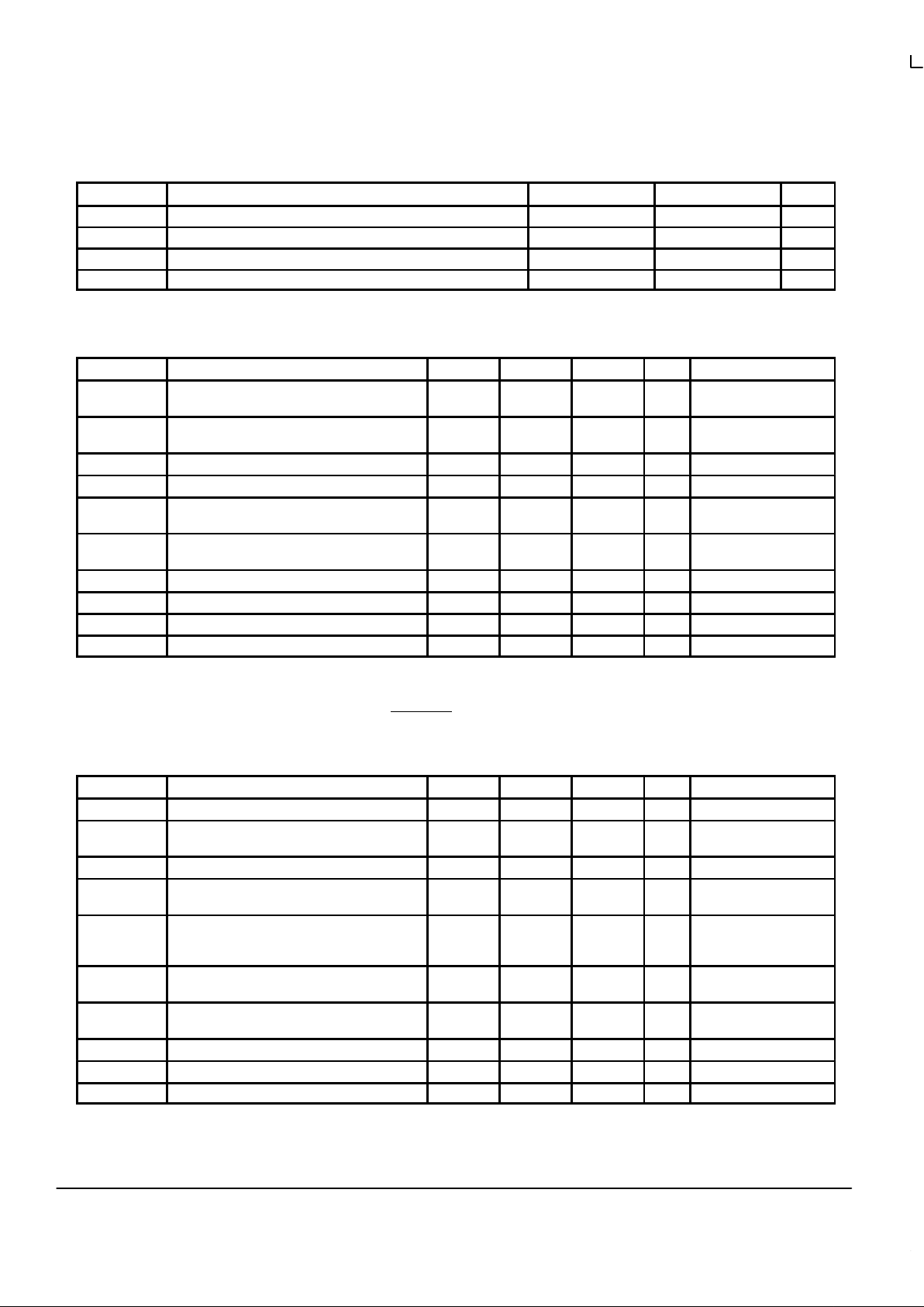
ABSOLUTE MAXIMUM RATINGS*
Symbol Parameter Min Max Unit
V
CC
Supply Voltage –0.3 4.6 V
V
I
Input Voltage –0.3 VDD + 0.3 V
I
IN
Input Current ±20 mA
T
Stor
Storage Temperature Range –40 125 °C
* Absolute maximum continuous ratings are those values beyond which damage to the device may occur. Exposure to these conditions or conditions beyond those
indicated may adversely affect device reliability. Functional operation under absolute–maximum–rated conditions is not implied.
DC CHARACTERISTICS (TA = 0° to 70°C, VCC = 3.3V ±0.3V)
Symbol Characteristic Min Typ Max Unit Condition
V
IH
Input HIGH Voltage PECL_CLK
Other
2.135
2.0
2.42
3.60
V Single Ended Spec
V
IL
Input LOW Voltage PECL_CLK
Other
1.49 1.825
0.8
V Single Ended Spec
V
PP
Peak–to–Peak Input Voltage PECL_CLK 300 1000 mV
V
CMR
Common Mode Range PECL_CLK VCC – 2.0 VCC – 0.6 V Note NO TAG
V
OH
Output HIGH Voltage 2.5 V IOH = –20mA (Note
NO TAG)
V
OL
Output LOW Voltage 0.4 V IOL = 20mA (Note
NO TAG)
I
IN
Input Current ±100 µA Note NO TAG
C
IN
Input Capacitance 4 pF
C
pd
Power Dissipation Capacitance 25 pF Per Output
I
CC
Maximum Quiescent Supply Current 22 30 mA
1. V
CMR
is the difference from the most positive side of the differential input signal. Normal operation is obtained when the “HIGH” input is within
the V
CMR
range and the input swing lies within the VPP specification.
2. The MPC948 outputs can drive series or parallel terminated 50Ω (or 50Ω to VCC/2) transmission lines on the incident edge (see Applications
Info section).
3. Inputs have pull–up resistors which affect input current, PECL_CLK
has a pull–down resistor.
AC CHARACTERISTICS (TA = 0° to 70°C, VCC = 3.3V ±0.3V)
Symbol Characteristic Min Typ Max Unit Condition
F
max
Maximum Input Frequency 150 MHz Note NO TAG
t
pd
Propagation Delay PECL_CLK to Q
TTL_CLK to Q
4.0
4.4
8.0
8.9
ns Note NO TAG
t
sk(o)
Output–to–Output Skew 350 ps Note NO TAG
t
sk(pr)
Part–to–Part Skew PECL_CLK to Q
TTL_CLK to Q
1.5
2.0
ns Notes NO TAG,
NO TAG
t
pwo
Output Pulse Width t
CYCLE
/2 –
800
t
CYCLE
/2 +
800
ps Notes NO TAG,
NO TAG
Measured at VCC/2
t
s
Setup Time Sync_OE to PECL_CLK
Sync_OE to TTL_CLK
1.0
0.0
ns Notes NO TAG,
NO TAG
t
h
Hold Time PECL_CLK to Sync_OE
TTL_CLK to Sync_OE
0.0
1.0
ns Notes NO TAG,
NO TAG
t
PZL,tPZH
Output Enable Time 3 11 ns
t
PLZ,tPHZ
Output Disable Time 3 11 ns
tr, t
f
Output Rise/Fall Time 0.20 1.0 ns 0.8V to 2.0V
4. Driving 50Ω transmission lines
5. Part–to–part skew at a given temperature and voltage
6. Assumes 50% input duty cycle.
7. Setup and Hold times are relative to the falling edge of the input clock
Page 4
MPC948
MOTOROLA TIMING SOLUTIONS
BR1333 — Rev 6
4
APPLICATIONS INFORMATION
Driving Transmission Lines
The MPC948 clock driver was designed to drive high
speed signals in a terminated transmission line environment.
To provide the optimum flexibility to the user the output
drivers were designed to exhibit the lowest impedance
possible. With an output impedance of less than 10Ω the
drivers can drive either parallel or series terminated
transmission lines. For more information on transmission
lines the reader is referred to application note AN1091 in the
Timing Solutions brochure (BR1333/D).
In most high performance clock networks point–to–point
distribution of signals is the method of choice. In a
point–to–point scheme either series terminated or parallel
terminated transmission lines can be used. The parallel
technique terminates the signal at the end of the line with a
50Ω resistance to VCC/2. This technique draws a fairly high
level of DC current and thus only a single terminated line can
be driven by each output of the MPC948 clock driver. For the
series terminated case however there is no DC current draw,
thus the outputs can drive multiple series terminated lines.
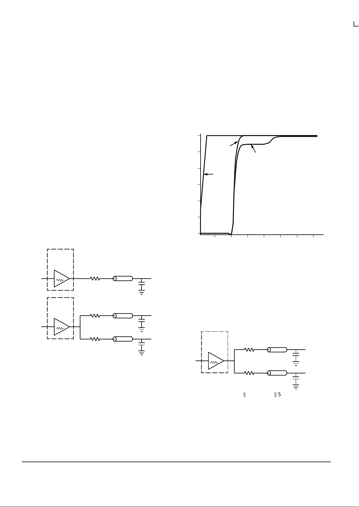
NO TAG illustrates an output driving a single series
terminated line vs two series terminated lines in parallel.
When taken to its extreme the fanout of the MPC948 clock
driver is effectively doubled due to its capability to drive
multiple lines.
Figure 4. Single versus Dual Transmission Lines
7
Ω
IN
MPC948
OUTPUT
BUFFER
RS = 43
Ω
ZO = 50
Ω
OutA
7
Ω
IN
MPC948
OUTPUT
BUFFER
RS = 43
Ω
ZO = 50
Ω
OutB0
RS = 43
Ω
ZO = 50
Ω
OutB1
The waveform plots of NO TAG show the simulation
results of an output driving a single line vs two lines. In both
cases the drive capability of the MPC948 output buffers is
more than sufficient to drive 50Ω transmission lines on the
incident edge. Note from the delay measurements in the
simulations a delta of only 43ps exists between the two
differently loaded outputs. This suggests that the dual line
driving need not be used exclusively to maintain the tight
output–to–output skew of the MPC948. The output waveform
in NO TAG shows a step in the waveform, this step is caused
by the impedance mismatch seen looking into the driver. The
parallel combination of the 43Ω series resistor plus the output
impedance does not match the parallel combination of the
line impedances. The voltage wave launched down the two
lines will equal:
VL = VS ( Zo / Rs + Ro +Zo) = 3.0 (25/53.5) = 1.40V
At the load end the voltage will double, due to the near
unity reflection coefficient, to 2.8V. It will then increment
towards the quiescent 3.0V in steps separated by one round
trip delay (in this case 4.0ns).
Figure 5. Single versus Dual Waveforms
TIME (nS)
VOLTAGE (V)
3.0
2.5
2.0
1.5
1.0
0.5
0
2 4 6 8 10 12 14
OutB
tD = 3.9386
OutA
tD = 3.8956
In
Since this step is well above the threshold region it will not
cause any false clock triggering, however designers may be
uncomfortable with unwanted reflections on the line. To
better match the impedances when driving multiple lines the
situation in NO TAG should be used. In this case the series
terminating resistors are reduced such that when the parallel
combination is added to the output buffer impedance the line
impedance is perfectly matched.
Figure 6. Optimized Dual Line Termination
7
Ω
MPC948
OUTPUT
BUFFER
RS = 36
Ω
ZO = 50
Ω
RS = 36
Ω
ZO = 50
Ω
7Ω + 36Ω k 36Ω = 50Ω k 50Ω
25Ω = 25Ω
SPICE level output buffer models are available for
engineers who want to simulate their specific interconnect
schemes. In addition IV characteristics are in the process of
being generated to support the other board level simulators in
general use.
Page 5
MPC948
TIMING SOLUTIONS
BR1333 — Rev 6
5 MOTOROLA
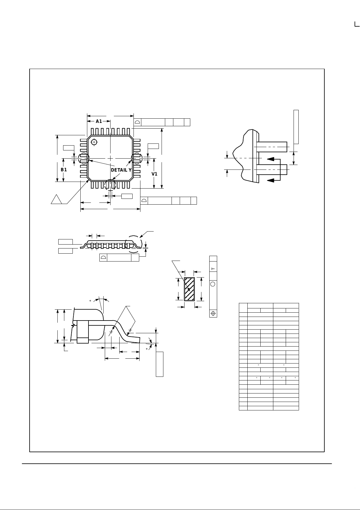
OUTLINE DIMENSIONS
FA SUFFIX
TQFP PACKAGE
CASE 873A–02
ISSUE A
DETAIL Y
A
S1
VB
1
8
9
17
25
32
AE
AE
P
DETAIL Y
BASE
N
J
DF
METAL
SECTION AE–AE
G
SEATING
PLANE
R
Q
_
W
K
X
0.250 (0.010)
GAUGE PLANE
E
C
H
DETAIL AD
NOTES:
1. DIMENSIONING AND TOLERANCING PER ANSI
Y14.5M, 1982.
2. CONTROLLING DIMENSION: MILLIMETER.
3. DATUM PLANE –AB– IS LOCATED AT BOTTOM OF
LEAD AND IS COINCIDENT WITH THE LEAD
WHERE THE LEAD EXITS THE PLASTIC BODY AT
THE BOTTOM OF THE PARTING LINE.
4. DATUMS –T–, –U–, AND –Z– TO BE DETERMINED
AT DATUM PLANE –AB–.
5. DIMENSIONS S AND V TO BE DETERMINED AT
SEATING PLANE –AC–.
6. DIMENSIONS A AND B DO NOT INCLUDE MOLD
PROTRUSION. ALLOWABLE PROTRUSION IS
0.250 (0.010) PER SIDE. DIMENSIONS A AND B
DO INCLUDE MOLD MISMATCH AND ARE
DETERMINED AT DATUM PLANE –AB–.
7. DIMENSION D DOES NOT INCLUDE DAMBAR
PROTRUSION. DAMBAR PROTRUSION SHALL
NOT CAUSE THE D DIMENSION TO EXCEED
0.520 (0.020).
8. MINIMUM SOLDER PLATE THICKNESS SHALL BE
0.0076 (0.0003).
9. EXACT SHAPE OF EACH CORNER MAY VARY
FROM DEPICTION.
DIMAMIN MAX MIN MAX
INCHES
7.000 BSC 0.276 BSC
MILLIMETERS
B 7.000 BSC 0.276 BSC
C 1.400 1.600 0.055 0.063
D 0.300 0.450 0.012 0.018
E 1.350 1.450 0.053 0.057
F 0.300 0.400 0.012 0.016
G 0.800 BSC 0.031 BSC
H 0.050 0.150 0.002 0.006
J 0.090 0.200 0.004 0.008
K 0.500 0.700 0.020 0.028
M 12 REF 12 REF
N 0.090 0.160 0.004 0.006
P 0.400 BSC 0.016 BSC
Q 1 5 1 5
R 0.150 0.250 0.006 0.010
V 9.000 BSC 0.354 BSC
V1 4.500 BSC 0.177 BSC
__
____
DETAIL AD
A1
B1
V1
4X
S
4X
B1 3.500 BSC 0.138 BSC
A1 3.500 BSC 0.138 BSC
S 9.000 BSC 0.354 BSC
S1 4.500 BSC 0.177 BSC
W 0.200 REF 0.008 REF
X 1.000 REF 0.039 REF
9
–T–
–Z–
–U–
T–U0.20 (0.008) ZAC
T–U0.20 (0.008) ZAB
0.10 (0.004) AC
–AC–
–AB–
M
_
8X
–T–, –U–, –Z–
T–U
M
0.20 (0.008) ZAC
Page 6

MPC948
MOTOROLA TIMING SOLUTIONS
BR1333 — Rev 6
6
Motorola reserves the right to make changes without further notice to any products herein. Motorola makes no warranty , representation or guarantee regarding
the suitability of its products for any particular purpose, nor does Motorola assume any liability arising out of the application or use of any product or circuit, and
specifically disclaims any and all liability, including without limitation consequential or incidental damages. “T ypical” parameters which may be provided in Motorola
data sheets and/or specifications can and do vary in different applications and actual performance may vary over time. All operating parameters, including “Typicals”
must be validated for each customer application by customer’s technical experts. Motorola does not convey any license under its patent rights nor the rights of
others. Motorola products are not designed, intended, or authorized for use as components in systems intended for surgical implant into the body, or other
applications intended to support or sustain life, or for any other application in which the failure of the Motorola product could create a situation where personal injury
or death may occur. Should Buyer purchase or use Motorola products for any such unintended or unauthorized application, Buyer shall indemnify and hold Motorola
and its officers, employees, subsidiaries, affiliates, and distributors harmless against all claims, costs, damages, and expenses, and reasonable attorney fees
arising out of, directly or indirectly, any claim of personal injury or death associated with such unintended or unauthorized use, even if such claim alleges that
Motorola was negligent regarding the design or manufacture of the part. Motorola and are registered trademarks of Motorola, Inc. Motorola, Inc. is an Equal
Opportunity/Affirmative Action Employer.
How to reach us:
USA/EUROPE/ Locations Not Listed: Motorola Literature Distribution; JAPAN: Nippon Motorola Ltd.; Tatsumi–SPD–JLDC, 6F Seibu–Butsuryu–Center,
P.O. Box 5405; Denver, Colorado 80217. 303–675–2140 or 1–800–441–2447 3–14–2 T atsumi Koto–Ku, Tokyo 135, Japan. 81–3–3521–8315
Mfax: [email protected] – TOUCHTONE 602–244–6609 ASIA/PACIFIC: Motorola Semiconductors H.K. Ltd.; 8B Tai Ping Industrial Park,
INTERNET: http://www.mot.com/sps/ 51 Ting Ko k Road, Tai Po, N.T., Hong Kong. 852–26629298
MPC948/D
◊
 Loading...