

Page 1
SEMICONDUCTOR TECHNICAL DATA
1
REV 0.2
Motorola, Inc. 1997
6/97
"
!
The MPC940 is a 1:18 low voltage clock distribution chip. The device
features the capability to select either a differential L VPECL or an LVTTL/
LVCMOS compatible input. The 18 outputs are LVCMOS or LVTTL
compatible and feature the drive strength to drive 50Ω series or parallel
terminated transmission lines. With output–to–output skews of 150ps, the
MPC940 is ideal as a clock distribution chip for the most demanding of
synchronous systems. For a similar product with a larger number of
outputs, please consult the MPC941 data sheet.
• LVPECL or LVCMOS/LVTTL Clock Input
• 150ps Maximum Targeted Output–to–Output Skew
• Drives Up to 36 Independent Clock Lines
• Maximum Output Frequency of 250MHz
• 32–Lead TQFP Packaging
• 3.3V V
CC
Supply Voltage
With a low output impedance (≈20Ω), in both the HIGH and LOW logic
states, the output buffers of the MPC940 are ideal for driving series
terminated transmission lines. More specifically, each of the 18 MPC940
outputs can drive two series terminated 50Ω transmission lines. With this
capability, the MPC940 has an effective fanout of 1:36 in applications
where each line drives a single load. With this level of fanout, the
MPC940 provides enough copies of low skew clocks for most high
performance synchronous systems.
The differential LVPECL inputs of the MPC940 allow the device to interface directly with a LVPECL fanout buffer like the
MC100EP111 to build very wide clock fanout trees or to couple to a high frequency clock source. The LVCMOS/LVTTL input
provides a more standard interface for applications requiring only a single clock distribution chip at relatively low frequencies. In
addition, the two clock sources can be used to provide for a test clock interface as well as the primary system clock. A logic HIGH
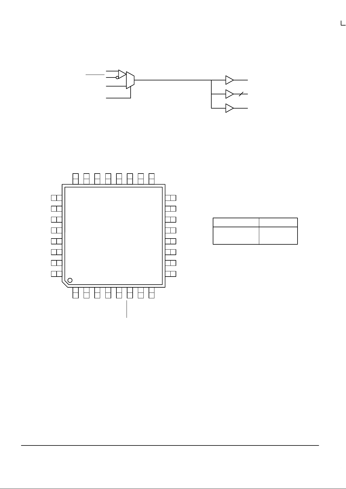
on the LVCMOS_CLK_Sel pin will select the TTL level clock input.
The MPC940 is fully 3.3V compatible. The 32–lead TQFP package was chosen to optimize performance, board space and
cost of the device. The 32–lead TQFP has a 7x7mm body size with a conservative 0.8mm pin spacing.
This document contains information on a new product. Specifications and information herein are subject to
change without notice.
LOW VOLTAGE
1:18 CLOCK
DISTRIBUTION CHIP
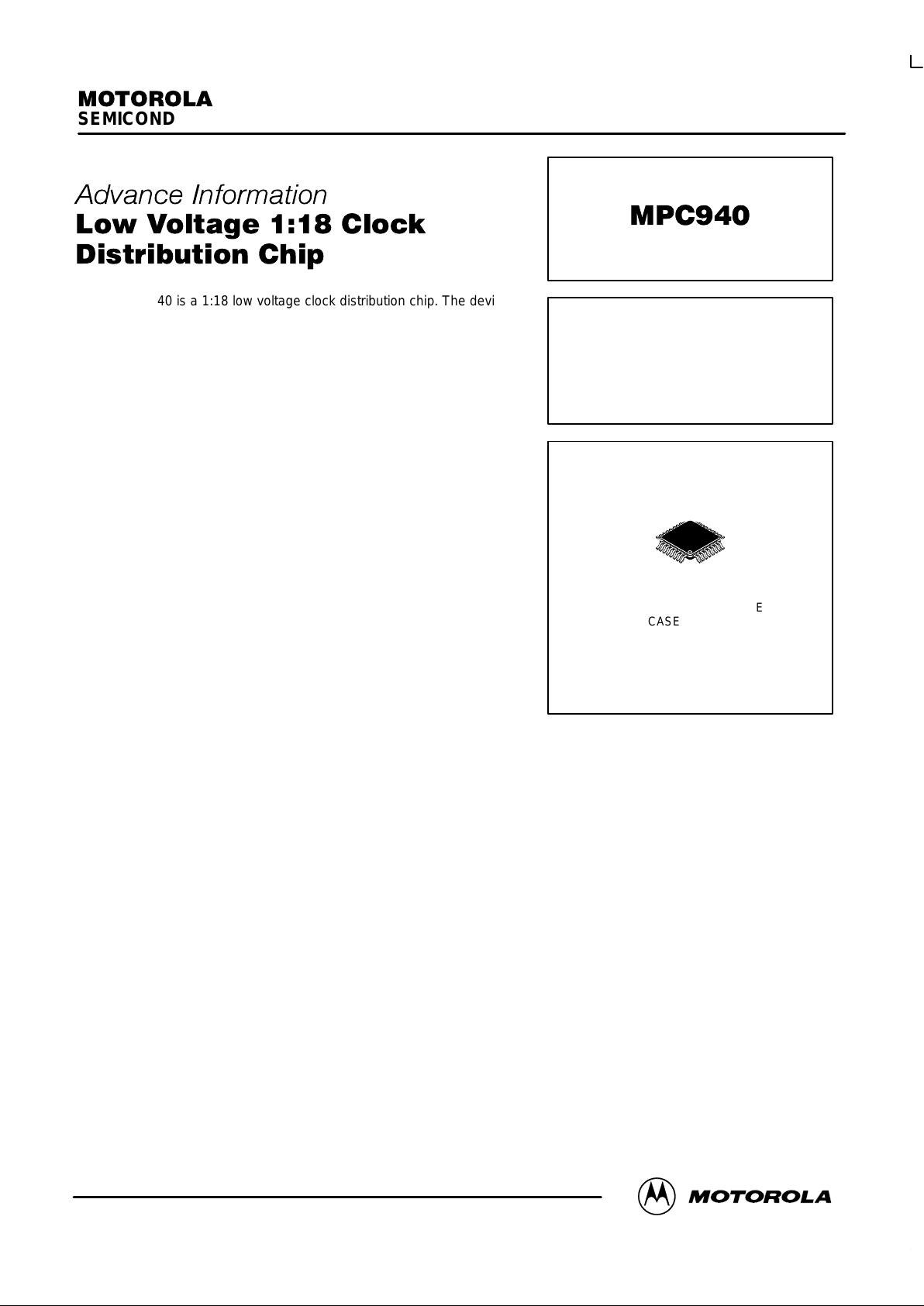
FA SUFFIX
32–LEAD TQFP PACKAGE
CASE 873A–02
Page 2
MPC940
MOTOROLA TIMING SOLUTIONS
BR1333 — Rev 6
2
Pinout: 32–Lead TQFP (Top View)
FUNCTION TABLE
LVCMOS_CLK_Sel Input
0
1
PECL_CLK
LVCMOS_CLK
LOGIC DIAGRAM
LVCMOS_CLK
Q0
PECL_CLK
0
1
LVCMOS_CLK_Sel
PECL_CLK
GNDO
Q5
Q4
Q3
VCCO
Q2
Q1
Q0
VCCO
Q12
Q13
Q14
GNDO
Q15
Q16
Q17
Q6
Q7
Q8
VCCOQ9Q10
Q11
GND
GNDO
GNDI
VCCI
LVCMOS_CLK
LVCMOS_CLK_Sel
PECL_CLK
PECL_CLK
VCCO
25
26
27
28
29
30
31
32
15
14
13
12
11
10
9
12345678
24 23 22 21 20 19 18 17
16
MPC940
Q1–Q16
16
Q17
Page 3

MPC940
TIMING SOLUTIONS
BR1333 — Rev 6
3 MOTOROLA
ABSOLUTE MAXIMUM RATINGS*
Symbol Parameter Min Max Unit
V
CC
Supply Voltage –0.3 3.6 V
V
I
Input Voltage –0.3 VDD + 0.3 V
I
IN
Input Current ±20 mA
T
Stor
Storage Temperature Range –40 125 °C
* Absolute maximum continuous ratings are those values beyond which damage to the device may occur. Exposure to these conditions or conditions beyond those
indicated may adversely affect device reliability. Functional operation under absolute–maximum–rated conditions is not implied.
DC CHARACTERISTICS (TA = 0° to 70°C, VCC = 3.3V ±5%)
Symbol Characteristic Min Typ Max Unit Condition
V
IH
Input HIGH Voltage PECL_CLK
Other
2.135
2.0
2.42
3.60
V
V
IL
Input LOW Voltage PECL_CLK
Other
1.49 1.825
0.8
V
V
PP
Peak–to–Peak Input Voltage PECL_CLK 300 1000 mV
V
CMR
Common Mode Range PECL_CLK VCC–2.0 VCC–0.6 V
V
OH
Output HIGH Voltage 2.5 V IOH = –16mA, Note 1.
V
OL
Output LOW Voltage 0.5 V IOH = 16mA, Note 1.
I
IN
Input Current ±100 µA
C
IN
Input Capacitance 4 pF
C
pd
Power Dissipation Capacitance 8 pF Per Output
I
CC
Maximum Quiescent Supply Current I
CCL
I
CCH
70
140
mA
1. The MPC940 outputs can drive series or parallel terminated 50Ω (or 50Ω to VCC/2) transmission lines on the incident edge.
AC CHARACTERISTICS (TA = 0° to 70°C, VCC = 3.3V ±5%)
Symbol Characteristic Min Typ Max Unit Condition
F
max
Maximum Input Frequency 250 MHz Note 1.
t
pd
Propagation Delay PECL_CLK to Q
TTL_CLK to Q
1.7
2.0
ns Note 1.
t
sk(o)
Output–to–Output Skew 150 ps Note 1.
t
sk(pr)
Part–to–Part Skew PECL_CLK to Q
TTL_CLK to Q
800
800
ps Notes 2., 3.
t
pwo
Output Pulse Width 45 55 p% Note 1.,
Measured at VCC/2
tr, t
f
Output Rise/Fall Time 0.20 1.0 ns 0.8V to 2.0V
1. Driving 50Ω transmission lines
2. Part–to–part skew at a given temperature and voltage
3. Final specification limits will be determined from matrix lot material. 800ps is the “best estimate” based on initial material and experience with
previous products.
Page 4

MPC940
MOTOROLA TIMING SOLUTIONS
BR1333 — Rev 6
4
OUTLINE DIMENSIONS
FA SUFFIX
TQFP PACKAGE
CASE 873A–02
ISSUE A
DETAIL Y
A
S1
VB
1
8
9
17
25
32
AE
AE
P
DETAIL Y
BASE
N
J
DF
METAL
SECTION AE–AE
G
SEATING
PLANE
R
Q
_
W
K
X
0.250 (0.010)
GAUGE PLANE
E
C
H
DETAIL AD
NOTES:
1. DIMENSIONING AND TOLERANCING PER ANSI
Y14.5M, 1982.
2. CONTROLLING DIMENSION: MILLIMETER.
3. DATUM PLANE –AB– IS LOCATED AT BOTTOM OF
LEAD AND IS COINCIDENT WITH THE LEAD
WHERE THE LEAD EXITS THE PLASTIC BODY AT
THE BOTTOM OF THE PARTING LINE.
4. DATUMS –T–, –U–, AND –Z– TO BE DETERMINED
AT DATUM PLANE –AB–.
5. DIMENSIONS S AND V TO BE DETERMINED AT
SEATING PLANE –AC–.
6. DIMENSIONS A AND B DO NOT INCLUDE MOLD
PROTRUSION. ALLOWABLE PROTRUSION IS
0.250 (0.010) PER SIDE. DIMENSIONS A AND B
DO INCLUDE MOLD MISMATCH AND ARE
DETERMINED AT DATUM PLANE –AB–.
7. DIMENSION D DOES NOT INCLUDE DAMBAR
PROTRUSION. DAMBAR PROTRUSION SHALL
NOT CAUSE THE D DIMENSION TO EXCEED
0.520 (0.020).
8. MINIMUM SOLDER PLATE THICKNESS SHALL BE
0.0076 (0.0003).
9. EXACT SHAPE OF EACH CORNER MAY VARY
FROM DEPICTION.
DIMAMIN MAX MIN MAX
INCHES
7.000 BSC 0.276 BSC
MILLIMETERS
B 7.000 BSC 0.276 BSC
C 1.400 1.600 0.055 0.063
D 0.300 0.450 0.012 0.018
E 1.350 1.450 0.053 0.057
F 0.300 0.400 0.012 0.016
G 0.800 BSC 0.031 BSC
H 0.050 0.150 0.002 0.006
J 0.090 0.200 0.004 0.008
K 0.500 0.700 0.020 0.028
M 12 REF 12 REF
N 0.090 0.160 0.004 0.006
P 0.400 BSC 0.016 BSC
Q 1 5 1 5
R 0.150 0.250 0.006 0.010
V 9.000 BSC 0.354 BSC
V1 4.500 BSC 0.177 BSC
__
____
DETAIL AD
A1
B1
V1
4X
S
4X
B1 3.500 BSC 0.138 BSC
A1 3.500 BSC 0.138 BSC
S 9.000 BSC 0.354 BSC
S1 4.500 BSC 0.177 BSC
W 0.200 REF 0.008 REF
X 1.000 REF 0.039 REF
9
–T–
–Z–
–U–
T–U0.20 (0.008) ZAC
T–U0.20 (0.008) ZAB
0.10 (0.004) AC
–AC–
–AB–
M
_
8X
–T–, –U–, –Z–
T–U
M
0.20 (0.008) ZAC
Page 5

MPC940
TIMING SOLUTIONS
BR1333 — Rev 6
5 MOTOROLA
Motorola reserves the right to make changes without further notice to any products herein. Motorola makes no warranty , representation or guarantee regarding
the suitability of its products for any particular purpose, nor does Motorola assume any liability arising out of the application or use of any product or circuit, and
specifically disclaims any and all liability, including without limitation consequential or incidental damages. “T ypical” parameters which may be provided in Motorola
data sheets and/or specifications can and do vary in different applications and actual performance may vary over time. All operating parameters, including “Typicals”
must be validated for each customer application by customer’s technical experts. Motorola does not convey any license under its patent rights nor the rights of
others. Motorola products are not designed, intended, or authorized for use as components in systems intended for surgical implant into the body, or other
applications intended to support or sustain life, or for any other application in which the failure of the Motorola product could create a situation where personal injury
or death may occur. Should Buyer purchase or use Motorola products for any such unintended or unauthorized application, Buyer shall indemnify and hold Motorola
and its officers, employees, subsidiaries, affiliates, and distributors harmless against all claims, costs, damages, and expenses, and reasonable attorney fees
arising out of, directly or indirectly, any claim of personal injury or death associated with such unintended or unauthorized use, even if such claim alleges that
Motorola was negligent regarding the design or manufacture of the part. Motorola and are registered trademarks of Motorola, Inc. Motorola, Inc. is an Equal
Opportunity/Affirmative Action Employer.
MPC940/D
◊
Mfax is a trademark of Motorola, Inc.
How to reach us:
USA/EUROPE/Locations Not Listed: Motorola Literature Distribution; JAPAN: Nippon Motorola Ltd.: SPD, Strategic Planning Office, 4–32–1,
P.O. Box 5405, Denver, Colorado 80217. 303–675–2140 or 1–800–441–2447 Nishi–Gotanda, Shinagawa–ku, Tokyo 141, Japan. 81–3–5487–8488
Mfax: RMFAX0@email.sps.mot.com – TOUCHTONE 602–244–6609 ASIA/PACIFIC: Motorola Semiconductors H.K. Ltd.; 8B Tai Ping Industrial Park,
– US & Canada ONLY 1–800–774–1848 51 Ting Kok Road, Ta i Po, N.T., Hong Kong. 852–26629298
INTERNET: http://motorola.com/sps
 Loading...