

Page 1
SEMICONDUCTOR TECHNICAL DATA
1
REV 0.2
Motorola, Inc. 1997
6/97
The MPC9140 is a 1:18 LVCMOS fanout buffer targeted to support
Intel based Pentium II microprocessor chip sets. The device features
18 low skew outputs optimized to drive the clock inputs of standard
unbuffered SDRAM modules. Standard unbuffered SDRAM modules
require four clocks per module allowing for the device to drive up to four
modules. The output buffers have been optimized to drive the load
presented by the SDRAM module.
The MPC9140 provides output shut off capabilities via an I2C serial
port for applications which plan to use fewer than four modules and desire
to minimize the power dissipation of the chip. Every output clock can be
individually enabled/disabled through fields in the I2C control registers.
After power up the default state is all outputs enabled. In applications
where this default state is acceptable the I2C ports need not be exercised.
• Supports Intel Pentium and Pentium II Processor Architectures
• 18 Skew Controlled 3.3V Compatible SDRAM Clocks
• I
2
C Serial Bus Interface
• Extensive Output Enable Control Capability
• Space Efficient 48–Lead SSOP Package
• Operating Temperature Range of 0°C to 70°C
• 3.3V ± 5% Power Supply
481
NCNC
472
NCNC
463
VDDVDD
454
SDRAM15SDRAM0
445
SDRAM14SDRAM1
436
VSSVSS
427
VDDVDD
418
SDRAM13SDRAM2
409
SDRAM12SDRAM3
3910
VSSVSS
3811
OEBUF_IN
3712
VDDVDD2
3613
SDRAM11SDRAM4
3514
SDRAM10SDRAM5
3415
VSS
VSS
3316
VDDVDD
3217
SDRAM9SDRAM6
3118
SDRAM8SDRAM7
3019
VSSVSS
2920
VDDVDD
2821
SDRAM17SDRAM16
2722
VSSVSS
2623
VSS
VDD
2524
SCLOCKSDATA
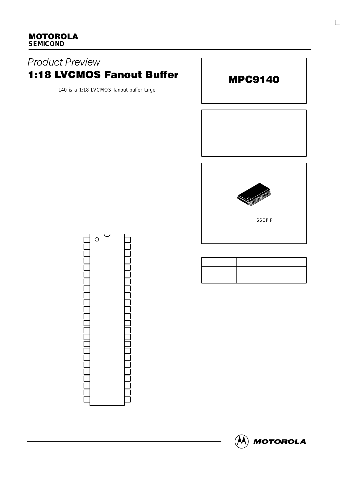
Figure 1. 48–Lead Pinout (Top View)
This document contains information on a product under development. Motorola reserves the right to change or
discontinue this product without notice.
1:18 LVCMOS
FANOUT BUFFER
SD SUFFIX
48–LEAD PLASTIC SSOP PACKAGE
CASE 1215–01
FUNCTION TABLE
OE V1, V2
0
1
High–Z
1x BUF_IN
Page 2
MPC9140
MOTOROLA TIMING SOLUTIONS
BR1333 — REV 5
2
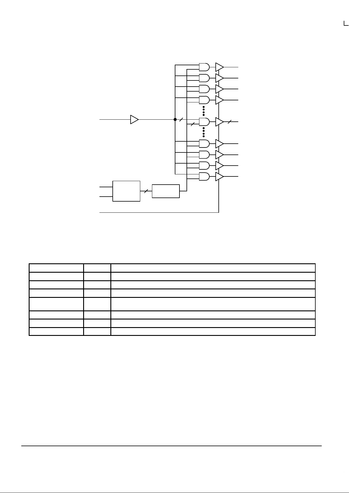
Figure 2. Block Diagram
SDRAM0
SDRAM1
SDRAM2
SDRAM3
SDRAM4:13
SDRAM14
SDRAM15
SDRAM16
SDRAM17
CONFIG
REGISTERS
I2C
INTERFACE
SDATA
SCLOCK
OE
18
10
10
10
BUF_IN
Table 1. Pin Descriptions
Pin Name I/O Function
BUF_IN I 3.3V CMOS clock input
SDRAM0:17 O 3.3V CMOS SDRAM clock outputs
SDATA I/O Serial data for configuration control
SCLK I Serial clock input for configuration control. The state of the SDATA input is clocked into the device on
the rising edge of this clock
OE I A Low forces all outputs into High–Z state
VDD – 3.3V power supply connection
VSS – Ground connection which should be connected directly to the ground plane
Page 3

MPC9140
TIMING SOLUTIONS
BR1333 — REV 5
3 MOTOROLA
I2C Interface
The device has an I2C serial bus interface consisting of a
serial clock input (SCLK) and a data line (SDATA) . The clock
driver acts as a slave receiver on the I2C bus with a standard
data transfer rate of up to 100 kbit/s. The MPC9140 is a ‘write
only’ device which will not respond to general call requests
from the bus master. The I2C interface transfers data in byte
length packets except for the start, stop and acknowledge
bits. The clock driver supports block writes consisting of the
following elements.
1) Start Bit
2) Address
3) Acknowledge Bit
4) Command Code
5) Acknowledge Bit
6) Byte Count
7) Acknowledge Bit
8) Data Fields (see Table 2)
9) Acknowledge Bit
10) Stop Bit
After each byte, the clock driver pulls down the data line to
acknowledge the transfer. The clock driver holds SDATA low
during the high state of SCLK. The 7–bit address of the clock
driver is:
A7 A6
A5 A4 A3 A2 A1 R/W
1 1 0 1 0 0 1 0
Note: A7 is the first address bit
The ‘Command Code’ should be set to all ‘0’s and the
‘Byte Count’ can range from 1 to 3. The data fields are
transferred sequentially in ascending order starting with Byte
0 – Configuration Function.
The MPC9140 is compliant with the DC/AC
characteristics of a “Standard–Mode” I2C bus device. The
logic thresholds are dependent on the 3.3V supply. For
additional information on the I2C bus, refer to the document,
3114 – “The I2C–bus and how to use it (including
specifications)” available from Philips Semiconductors:
http://www.semiconductors.philips.com
Table 2. Serial Data Fields
Byte Function Bit 7 Bit 6 Bit 5 Bit 4 Bit 3 Bit 2 Bit 1 Bit 0
SDRAM0:7 SDRAM7 SDRAM6 SDRAM5 SDRAM4 SDRAM3 SDRAM2 SDRAM1 SDRAM0
0
Package Pin 18 17 14 13 9 8 5 4
SDRAM8:15 SDRAM15 SDRAM14 SDRAM13 SDRAM12 SDRAM11 SDRAM10 SDRAM9 SDRAM8
1
Package Pin 45 44 41 40 36 35 32 31
SDRAM16:17 SDRAM17 SDRAM16 N/A N/A N/A N/A N/A N/A
2
Package Pin 28 21
1. Not Applicable (N/A) bits fields are “Don’t Care” conditions.
2. When a bit field is programmed with a “1” (enable), the clock is active. A “0” (disable) means the clock is inactive.
MAXIMUM RATINGS*
Symbol Parameter Min Max Unit
VDD 3.3V Core Supply Voltage –0.5 4.6 V
T
stg
Storage Temperature Range –65 150 °C
V
IH
3.3V Input High Voltage (Note 3.) –0.5 4.6 V
V
IL
3.3V Input Low Voltage –0.5 V
ESD ESD Input Protection 2000 V
* Maximum Ratings are those values beyond which damage to the device may occur. Functional operation should be restricted to the
Recommended Operating Conditions.
3. VIH should not exceed VDD level.
Page 4

MPC9140
MOTOROLA TIMING SOLUTIONS
BR1333 — REV 5
4
DC CHARACTERISTICS (VDD = 3.3V ±5%; GND = 0.0V; TA = 0 to +70°C; Unless Otherwise Specified)
Symbol Characteristic Min Typ Max Unit Condition
I
DD
Supply Current for VDD TBD mA
V
IL
Input Low Voltage –0.3 0.8 V
V
IH
Input High Voltage 2.0 VDD+0.3 V
I
IL
Input Leakage Current –5.0 5 µA 0 < VIN < VCC/VCCI
V
OL
3.3V Output Low Voltage 0.40 V IOL = 1mA
V
OH
3.3V Output High Voltage 2.4 V IOH = –1.0mA
C
I
Input Capacitance TBD pF Except XTL_In, XTL_Out
L
I
Input Inductance TBD nH Except XTL_In, XTL_Out
AC CHARACTERISTICS (VDD = 3.3V ±5%; GND = 0.0V; TA = 0 to +70°C; Unless Otherwise Specified)
Symbol Characteristic Min Typ Max Unit Condition
SDRAM Clock Outputs (SDRAM0:17)
t
sk
Output Clock Skew 250 ps Note 4.
d
t
Output Duty Cycle 45 55 % Note 5.
t
p
Clock Period 66MHz
100MHz
15.0
10.0
15.5
10.5
ns Note 4.
t
VIH
High Time 66MHz
100MHz
5.6
3.3
ns Measured at 2.4V
t
VIL
Low Time 66MHz
100MHz
5.3
3.1
ns Measured at 0.4V
t
rise
Rise Time 1.5 4.0 V/ns From 0.4V to 2.4V
t
fall
Fall Time 1.5 4.0 V/ns From 2.4V to 0.4V
t
PLH
Low to High Propagation Delay 1.0 5.0 ns
t
PHL
High to Low Propagation Delay 1.0 5.0 ns
t
PZL
,
t
PZH
Enable Delay 1.0 8.0 ns
t
PLZ
,
t
PHZ
Disable Delay 1.0 8.0 ns
4. Measured on the rising edge of the clock at 1.5V .
5. Input slew rate >1V/ns.
Page 5

MPC9140
TIMING SOLUTIONS
BR1333 — REV 5
5 MOTOROLA
APPLICATIONS INFORMATION
Output Series Termination
With typical MPC9140 edge rates of 1.5V/ns, a PCB trace
becomes a transmission line when it is over 1–inch in length.
This transmission line needs some sort of termination
scheme to ensure good signal integrity at the load (device
receiving clock signal). Most motherboards use the practice
of
series termination
. In series termination, a series
termination resistor (external resistor) is added in series with
the driver device output, as shown in Figure 3, series
termination resistor value is chosen so that its value, added
to the output impedance of the driver, is equal to the PCB
trace impedance, or in other words,
RTH = RS + Z
L
. The
series termination resistor must be located close to the
device output.
Typical system PCB trace impedance is 50–70Ω, which is
low enough to produce sufficient signal rise and fall time at
the load capacitance presented by a standard CMOS input.
Figure 4 illustrates proper series termination of the 15Ω
MPC9140 output driving a 60Ω transmission line.
Figure 3. Clock Output Series Termination
Output Buffer Model
R
TH
R
S
Series
Termination
Resistor
Z
L
Transmission Line
(PCB Clock Trace)
Figure 4. Clock Output Series Termination
Output Buffer Model
15
Ω
45
Ω
Series
Termination
Resistor
60
Ω
Transmission Line
(PCB Clock Trace)
Pull–Up
Voltage
(V)
I
min
(mA)
I
typ
(mA)
I
max
(mA)
0 –72 –116 –198
1.000 –72 –116 –198
1.400 –68 –110 –188
1.500 –67 –107 –184
1.650 –64 –103 –177
1.800 –60 –98 –170
2.000 –54 –90 –157
2.400 –39 –69 –126
2.600 –30 –56 –107
3.135 0 –15 –46
3.300 – 0 –23
3.465 – – 0
Pull–Down
Voltage
(V)
I
min
(mA)
I
typ
(mA)
I
max
(mA)
0 0 0 0
0.400 23 34 53
0.650 35 52 83
0.850 43 65 104
1.000 49 74 118
1.400 61 93 152
1.500 64 98 159
1.650 67 103 168
1.800 70 108 177
1.950 72 112 184
3.315 72 112 204
3.600 – 112 204
Figure 5. Typical Output V/I Characteristics for MPC9140
Page 6

MPC9140
MOTOROLA TIMING SOLUTIONS
BR1333 — REV 5
6
OUTLINE DIMENSIONS
SD SUFFIX
PLASTIC SSOP PACKAGE
CASE 1215–01
ISSUE O
A
DIM MIN MAX
INCHES
A 0.095 0.110
A1 0.008 0.016
D 0.620 0.630
E 0.400 0.410
E1 0.292 0.299
L 0.024 0.040
b 0.008 0.0135
b1 0.008 0.012
c 0.005 0.010
c1 0.005 0.0085
e 0.025 BSC
1 0 8
M
0.004 CSB
S
A
C0.008 BA
C0.004
0.010
NOTES:
1. DIMENSIONS ARE IN INCH.
2. INTERPRET DIMENSIONS AND TOLERANCES
PER ASME Y14.5M, 1994.
3. DIMENSION D DOES NOT INCLUDE MOLD FLASH,
PROTRUSIONS OR GATE BURRS. MOLD FLASH
OR GATE BURRS SHALL NOT EXCEED 0.006 PER
SIDE.
4. DIMENSION E1 DOES NOT INCLUDE INTERLEAD
FLASH OR PROTRUSION. INTERLEAD FLASH OR
PROTRUSION SHALL NOT EXCEED 0.010 PER
SIDE.
5. DIMENSION b DOES NOT INCLUDE DAMBAR
PROTRUSION/INTRUSION. ALLOWABLE DAMBAR
PROTRUSIONS SHALL BE 0.003 TOTAL IN
EXCESS OF b DIMENSION AT MAXIMUM
MATERIAL CONDITION. DAMBAR INTRUSION
SHALL NOT REDUCE DIMENSION b BY MORE
THAN 0.003 AT LEAST MATERIAL CONDITION.
6. TERMINAL NUMBERS ARE SHOWN FOR
REFERENCE ONLY.
7. DIMENSION D AND E1 ARE TO BE DETERMINED
AT DATUM PLANE H.
48X b
E/2
E
PIN 1
IDENT
B
E1
D
48 25
124
C
e
A
A1
H
SEE DETAIL M
q
c
(b)
b1
SECTION N–N
L
DETAIL M
q
1
N
N
GAUGE
PLANE
__
c1
Pentium and Pentium II are trademarks of Intel Corp.
Motorola reserves the right to make changes without further notice to any products herein. Motorola makes no warranty , representation or guarantee regarding
the suitability of its products for any particular purpose, nor does Motorola assume any liability arising out of the application or use of any product or circuit, and
specifically disclaims any and all liability, including without limitation consequential or incidental damages. “T ypical” parameters which may be provided in Motorola
data sheets and/or specifications can and do vary in different applications and actual performance may vary over time. All operating parameters, including “Typicals”
must be validated for each customer application by customer’s technical experts. Motorola does not convey any license under its patent rights nor the rights of
others. Motorola products are not designed, intended, or authorized for use as components in systems intended for surgical implant into the body, or other
applications intended to support or sustain life, or for any other application in which the failure of the Motorola product could create a situation where personal injury
or death may occur. Should Buyer purchase or use Motorola products for any such unintended or unauthorized application, Buyer shall indemnify and hold Motorola
and its officers, employees, subsidiaries, affiliates, and distributors harmless against all claims, costs, damages, and expenses, and reasonable attorney fees
arising out of, directly or indirectly, any claim of personal injury or death associated with such unintended or unauthorized use, even if such claim alleges that
Motorola was negligent regarding the design or manufacture of the part. Motorola and are registered trademarks of Motorola, Inc. Motorola, Inc. is an Equal
Opportunity/Affirmative Action Employer.
MPC9140/D
◊
Mfax is a trademark of Motorola, Inc.
How to reach us:
USA/EUROPE/ Locations Not Listed: Motorola Literature Distribution; JAP AN: Nippon Motorola Ltd.: SPD, Strategic Planning Office, 4–32–1,
P.O. Box 5405, Denver, Colorado 80217. 303–675–2140 or 1–800–441–2447 Nishi–Gotanda, Shinagawa–ku, Tokyo 141, Japan. 81–3–5487–8488
Mfax: RMFAX0@email.sps.mot.com – TOUCHTONE 602–244–6609 ASIA/P ACIFIC: Motorola Semiconductors H.K. Ltd.; 8B Tai Ping Industrial Park,
– US & Canada ONLY 1–800–774–1848 51 Ting Kok Road, Tai Po, N.T., Hong Kong. 852–26629298
INTERNET: http://motorola.com/sps
 Loading...