

Page 1
SEMICONDUCTOR TECHNICAL DATA
1
REV 3
Motorola, Inc. 1996
10/96
! !
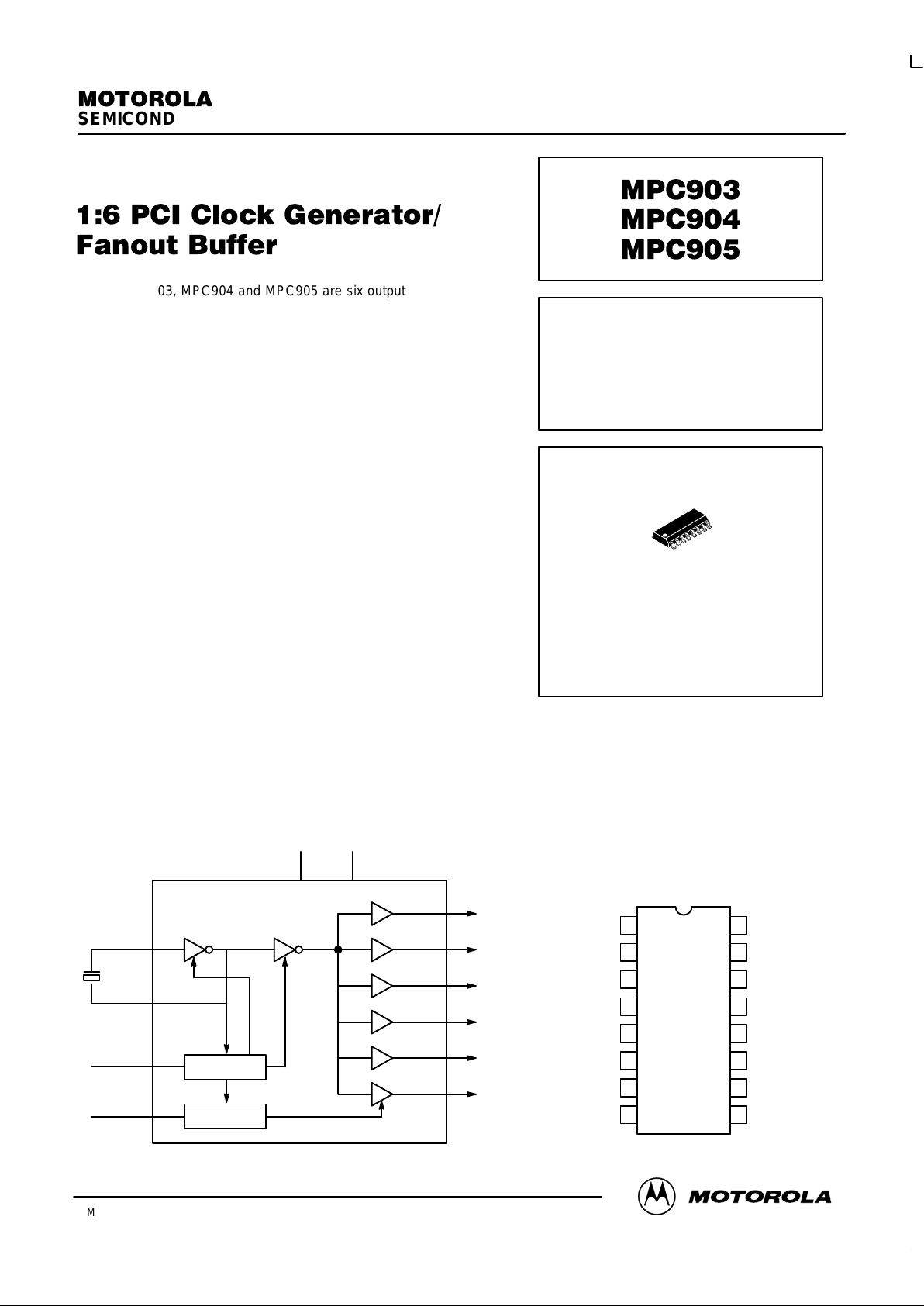
The MPC903, MPC904 and MPC905 are six output clock generation
devices targeted to provide the clocks required in a 3.3V or 5.0V PCI
environment. The device operates from a 3.3V supply and can interface
to either a TTL input or an external crystal. The inputs to the device can be
driven with 5.0V when the VCC is at 3.3V. The outputs of the
MPC903/904/905 meet all of the specifications of the PCI standard. The
three devices are identical except in the function of the Output Enables.
• Six Low Skew Outputs
• Synchronous Output Enables for Power Management
• Low Voltage Operation
• XTAL Oscillator Interface
• 16-Lead SOIC Package
• 5.0V Tolerant Enable Inputs
The MPC903/904/905 device is targeted for PCI bus or processor bus
environments with up to 12 clock loads. Each of the six outputs on the
MPC903/904/905 can drive two series terminated 50Ω transmission
lines. This capability effectively makes the MPC903/904/905 a 1:12
fanout buffer.
The MPC903 offers two synchronous enable inputs to allow users
flexibility in developing power management features for their designs.
Both enable signals are active HIGH inputs. A logic ‘0’ on the Enable1
input will pull all of the outputs into the logic ‘0’ state and shut down the
internal oscillator for a zero power sleep state. A logic ‘0’ on the Enable2
input will disable only the BCLK5 output. The Enable2 input can be used to disable any high power device for system power
savings during periods of inactivity. Both enable inputs are synchronized internal to the chip so that the output disabling will
happen only when the outputs are already LOW. This feature guarantees no runt pulses will be generated during enabling and
disabling. Note that when the MPC903 is re-enabled via the Enable1 pin, the user must allow for the oscillator to regain stability .
Thus, the re-enabling of the chip cannot occur instantaneously. The MPC904 and MPC905 Enable functions are slightly dif ferent
than the 903 and are outlined in the function tables on the following page.
BCLK0
BCLK1
BCLK2
BCLK3
BCLK4
BCLK5
XTAL_IN
XTAL_OUT
Enable1
Enable2
GND (3)VDD (3)
Pinout: 16-Lead Plastic Package (Top View)
161
152
143
134
XTAL_IN
Enable1
BCLK5
V
DD3
XTAL_OUT
Enable2
GND1
BCLK0
125
116
107
98
BCLK4
GND3
BCLK3
V
DD2
V
DD1
BCLK1
GND2
BCLK2
SYNCHRONIZE
SYNCHRONIZE
1:6 PCI
CLOCK GENERATOR/
FANOUT BUFFER
D SUFFIX
PLASTIC SOIC PACKAGE
CASE 751B-05
1
16
Page 2

MPC903 MPC904 MPC905
MOTOROLA TIMING SOLUTIONS
BR1333 — REV 5
2
FUNCTION TABLE
Outputs 0 to 4 Output 5 OSC (On/Off)
ENABLE1 ENABLE2 MPC903 MPC904 MPC905 MPC903 MPC904 MPC905 MPC903 MPC904 MPC905
0
0
1
1
0
1
0
1
Low
Low
Toggling
Toggling
Low
Low
Toggling
Toggling
Low
Low
Toggling
Toggling
Low
Low
Low
Toggling
Low
Toggling
Low
Toggling
Low
Toggling
Low
Toggling
OFF
OFF
ON
ON
OFF
ON
ON
ON
ON
ON
ON
ON
ABSOLUTE MAXIMUM RATINGS*
Symbol Parameter Min Max Unit
V
DD
Supply Voltage –0.5 4.6 V
V
IN
Input Voltage –0.5 VCC + 0.5 V
T
oper
Operating Temperature Range 0 +70 °C
T
stg
Storage Temperature Range –65 +150 °C
T
sol
Soldering Temperature Range (10 Sec) +260 °C
T
j
Junction Temperature Range +125 °C
P(E1=1) Power Dissipation TBD mW
P(E1=0) Power Dissipation 40 µW
ESD Static Discharge Voltage 2000 V
I
Latch
Latch Up Current 50 mA
* Absolute Maximum Ratings are those values beyond which damage to the device may occur. Functional operation should be restricted to the
Recommended Operating Conditions.
RECOMMENDED OPERATING CONDITIONS
Symbol Parameter Min Max Unit
T
A
Ambient Temperature Range 0 70 °C
V
DD
Positive Supply Voltage (Functional Range) 3.0 3.6 V
tDCin T
high
(at XTAL_IN Input)
T
low
(at XTAL_IN Input)
0.44T
1
0.44T
1
0.56T
1
0.56T
1
T = Period
1. When using External Source for reference, requirement to meet PCI clock duty cycle requirement on the output.
DC CHARACTERISTICS (TA = 0–70°C; VDD = 3.3V ±0.3V)
Symbol Characteristic Min Typ Max Unit Condition
V
IH
High Level Input Voltage 2.0 5.5
2
V
V
IL
Low Level Input Voltage 0.8 V
V
OH
High Level Output Voltage 2.4 V IOH = –36mA
1
V
OL
Low Level Output Voltage 0.4 V IOL = 36mA
1
I
IH
Input High Current 2.5
2
µA
I
IL
Input Low Current 2.5 µA
I
CC
Power Supply Current DC
33MHz
66MHz
20
37
78
45
95
µA
mA
mA
C
IN
Input Capacitance XTAL_IN
Others
9.0
4.5
pF
1. The MPC903/904/905 outputs can drive series terminated or parallel terminated 50Ω (or 50Ω to VCC/2) transmission lines on the incident edge
(see Applications Info).
2. XTAL_IN input will sink up to 10mA when driven to 5.5V . There are no reliability concerns associated with the condition. Note that the Enable1
input must be a logic HIGH. Do not take the Enable1 input to a logic LOW with >VCC volts on the XTAL_IN input.
Page 3

MPC903 MPC904 MPC905
TIMING SOLUTIONS
BR1333 — REV 5
3 MOTOROLA
AC CHARACTERISTICS (TA = 0–70°C; VDD = 3.3V ±0.3V)
Symbol Characteristic Min Typ Max Unit Condition
F
max
Maximum Operating Using External Crystal
Frequency Using External Clock Source
TBD
DC
50
100
MHz
t
pw
Output Pulse Width HIGH (Above 2.0V)
LOW (Below 0.8V)
HIGH (Above 2.0V)
LOW (Below 0.8V)
0.40T
1
0.40T
1
0.45T
2
0.45T
2
0.60T
1
0.60T
1
0.55T
2
0.55T
2
T = Periods
t
per
Output Period T – 400ps T = Desired Period
t
os
Output-to-Output Skew Rising Edges
Falling Edges
400
500
ps
tr, t
f
Rise/Fall Times (Slew Rate) 1 4 V/ns Series Terminated
Transmission Lines
t
EN
Enable Time Enable1
Enable2
5
4
ms
Cycles
t
DIS
Disable Time Enable1
Enable2
4
4
Cycles
A
osc
XTAL_IN to XTAL_OUT Oscillator Gain 6 db
Phase Loop Phase Shift Modulo 360° + 30 Degrees
1. Assuming input duty cycle specs from Recommended Operationg Conditions table are met.
2. Assuming external crystal or 50% duty cycle external reference is used.
Figure 1. Crystal Oscillator Interface
(Fundamental)
100
Ω
Pin 1Pin 16
Y1
33.3333MHz
16pF10pFC1 C3
Figure 2. Crystal Oscillator Interface
(3rd Overtone)
C
TRAP
Pin 1Pin 16
Y1
11.1111MHz
16pF10pFC1 C3
L
TRAP
f
FUND
+
1
2pL
TRAPCTRAP
Ǹ
Table 1. Crystal Specifications
Parameter Value
Crystal Cut Fundamental AT Cut
Resonance Parallel Resonance*
Frequency Tolerance ±75ppm at 25°C
Frequency/Temperature Stability ±150pm 0 to 70°C
Operating Range 0 to 70°C
Shunt Capacitance 5–7pF
Equivalent Series Resistance (ESR) 50 to 80Ω
Correlation Drive Level 100µW
Aging 5ppm/Yr (First 3 Y ears)
Page 4

MPC903 MPC904 MPC905
MOTOROLA TIMING SOLUTIONS
BR1333 — REV 5
4
BCLK0–4
BCLK5
ENABLE2
ENABLE1
Figure 3. Enable Timing Diagram
APPLICATIONS INFORMATION
Driving Transmission Lines
The MPC903/904/905 clock driver was designed to drive
high speed signals in a terminated transmission line
environment. T o provide the optimum flexibility to the user the
output drivers were designed to exhibit the lowest impedance
possible. With an output impedance of less than 10Ω the
drivers can drive either parallel or series terminated
transmission lines. For more information on transmission
lines the reader is referred to application note AN1091 in the
Timing Solutions brochure (BR1333/D).
In most high performance clock networks point–to–point
distribution of signals is the method of choice. In a
point–to–point scheme either series terminated or parallel
terminated transmission lines can be used. The parallel
technique terminates the signal at the end of the line with a
50Ω resistance to VCC/2. This technique draws a fairly high
level of DC current and thus only a single terminated line can
be driven by each output of the MPC903/904/905 clock
driver. For the series terminated case however there is no DC
current draw, thus the outputs can drive multiple series
terminated lines. Figure 4 illustrates an output driving a
single series terminated line vs two series terminated lines in
parallel. When taken to its extreme the fanout of the
MPC903/904/905 clock driver is effectively doubled due to its
capability to drive multiple lines.
Figure 4. Single versus Dual Transmission Lines
7
Ω
IN
MPC903
OUTPUT
BUFFER
RS = 43
Ω
ZO = 50
Ω
OutA
7
Ω
IN
MPC903
OUTPUT
BUFFER
RS = 43
Ω
ZO = 50
Ω
OutB0
RS = 43
Ω
ZO = 50
Ω
OutB1
The waveform plots of Figure 5 show the simulation
results of an output driving a single line vs two lines. In both
cases the drive capability of the MPC903/904/905 output
buffers is more than sufficient to drive 50Ω transmission lines
on the incident edge. Note from the delay measurements in
the simulations a delta of only 43ps exists between the two
differently loaded outputs. This suggests that the dual line
Page 5

MPC903 MPC904 MPC905
TIMING SOLUTIONS
BR1333 — REV 5
5 MOTOROLA
driving need not be used exclusively to maintain the tight
output–to–output skew of the MPC903. The output waveform
in Figure 5 shows a step in the waveform, this step is caused
by the impedance mismatch seen looking into the driver. The
parallel combination of the 43Ω series resistor plus the output
impedance does not match the parallel combination of the
line impedances. The voltage wave launched down the two
lines will equal:
VL = VS ( Zo / Rs + Ro +Zo) = 3.0 (25/53.5) = 1.40V
At the load end the voltage will double, due to the near
unity reflection coefficient, to 2.8V. It will then increment
towards the quiescent 3.0V in steps separated by one round
trip delay (in this case 4.0ns).
Figure 5. Single versus Dual Waveforms
TIME (nS)
VOLTAGE (V)
3.0
2.5
2.0
1.5
1.0
0.5
0
2 4 6 8 10 12 14
OutB
tD = 3.9386
OutA
tD = 3.8956
In
Since this step is well above the threshold region it will not
cause any false clock triggering, however designers may be
uncomfortable with unwanted reflections on the line. To
better match the impedances when driving multiple lines the
situation in Figure 6 should be used. In this case the series
terminating resistors are reduced such that when the parallel
combination is added to the output buffer impedance the line
impedance is perfectly matched.
Figure 6. Optimized Dual Line Termination
7
Ω
MPC903
OUTPUT
BUFFER
RS = 36
Ω
ZO = 50
Ω
RS = 36
Ω
ZO = 50
Ω
7Ω + 36Ω k 36Ω = 50Ω k 50Ω
25Ω = 25Ω
SPICE level output buffer models are available for
engineers who want to simulate their specific interconnect
schemes. In addition IV characteristics are in the process of
being generated to support the other board level simulators in
general use.
Page 6

MPC903 MPC904 MPC905
MOTOROLA TIMING SOLUTIONS
BR1333 — REV 5
6
OUTLINE DIMENSIONS
D SUFFIX
PLASTIC SOIC PACKAGE
CASE 751B-05
ISSUE J
NOTES:
1. DIMENSIONING AND TOLERANCING PER ANSI
Y14.5M, 1982.
2. CONTROLLING DIMENSION: MILLIMETER.
3. DIMENSIONS A AND B DO NOT INCLUDE
MOLD PROTRUSION.
4. MAXIMUM MOLD PROTRUSION 0.15 (0.006)
PER SIDE.
5. DIMENSION D DOES NOT INCLUDE DAMBAR
PROTRUSION. ALLOWABLE DAMBAR
PROTRUSION SHALL BE 0.127 (0.005) TOTAL
IN EXCESS OF THE D DIMENSION AT
MAXIMUM MATERIAL CONDITION.
18
16 9
SEATING
PLANE
F
J
M
R
X 45
_
G
8 PLP
–B–
–A–
M
0.25 (0.010) B
S
–T–
D
K
C
16 PL
S
B
M
0.25 (0.010) A
S
T
DIM MIN MAX MIN MAX
INCHESMILLIMETERS
A 9.80 10.00 0.386 0.393
B 3.80 4.00 0.150 0.157
C 1.35 1.75 0.054 0.068
D 0.35 0.49 0.014 0.019
F 0.40 1.25 0.016 0.049
G 1.27 BSC 0.050 BSC
J 0.19 0.25 0.008 0.009
K 0.10 0.25 0.004 0.009
M 0 7 0 7
P 5.80 6.20 0.229 0.244
R 0.25 0.50 0.010 0.019
____
Motorola reserves the right to make changes without further notice to any products herein. Motorola makes no warranty , representation or guarantee regarding
the suitability of its products for any particular purpose, nor does Motorola assume any liability arising out of the application or use of any product or circuit, and
specifically disclaims any and all liability, including without limitation consequential or incidental damages. “T ypical” parameters which may be provided in Motorola
data sheets and/or specifications can and do vary in different applications and actual performance may vary over time. All operating parameters, including “Typicals”
must be validated for each customer application by customer’s technical experts. Motorola does not convey any license under its patent rights nor the rights of
others. Motorola products are not designed, intended, or authorized for use as components in systems intended for surgical implant into the body, or other
applications intended to support or sustain life, or for any other application in which the failure of the Motorola product could create a situation where personal injury
or death may occur. Should Buyer purchase or use Motorola products for any such unintended or unauthorized application, Buyer shall indemnify and hold Motorola
and its officers, employees, subsidiaries, affiliates, and distributors harmless against all claims, costs, damages, and expenses, and reasonable attorney fees
arising out of, directly or indirectly, any claim of personal injury or death associated with such unintended or unauthorized use, even if such claim alleges that
Motorola was negligent regarding the design or manufacture of the part. Motorola and are registered trademarks of Motorola, Inc. Motorola, Inc. is an Equal
Opportunity/Affirmative Action Employer.
How to reach us:
USA/EUROPE /Locations Not Listed: Motorola Literature Distribution; JAPAN: Nippon Motorola Ltd.; Tatsumi–SPD–JLDC, 6F Seibu–Butsuryu–Center,
P.O. Box 20912; Phoenix, Arizona 85036. 1–800–441–2447 or 602–303–5454 3–14–2 Tatsumi Koto–Ku, Tokyo 135, Japan. 03–81–3521–8315
MFAX: RMF AX0@email.sps.mot.com – T OUCHTONE 602–244–6609 ASIA/PACIFIC: Motorola Semiconductors H.K. Ltd.; 8B Tai Ping Industrial Park,
INTERNET: http://Design–NET.com 51 Ting Kok Road, Tai Po, N.T., Hong Kong. 852–26629298
MPC903/D
*MPC903/D*
◊
 Loading...