

Page 1

MPC2104P•MPC2105P
1
MOTOROLA FAST SRAM
Product Preview
256KB/512KB BurstRAM
Secondary Cache Modules for
PowerPC PReP/CHRP Platforms
The MPC2104P (256KB) and MPC2105P (512KB) are designed to provide
burstable, high performance L2 cache for the PowerPC 60x microprocessor family
in conformance with the PowerPC Reference Platform (PReP) and the PowerPC
Common Hardware Reference Platform (CHRP) specifications.
The MPC2104P and MPC2105P utilize synchronous BurstRAMs. The MPC2104P
module is configured as 32K x 64 bits and uses two of the 3.3 V 32K x 32 data RAMs.
The MPC2105P is configured as 64K x 64 bits and uses two of the 3.3 V 64K x 32
data RAMs. Both modules are in a 178 (89 x 2) pin DIMM format. For tag bits on the
2104P, a 5 V cache tag RAM configured as 8K x 14 for tag field plus 8K x 2 for valid
and dirty status bits is used. For tag bits on the 2105P, a 5 V cache tag RAM
configured as 16K x 14 for tag field plus 16K x 2 for valid and dirty status bits is used.
Bursts can be initiated with the ADS
signal. Subsequent burst addresses are
generated internally to the BurstRAM by the CNTEN
signal.
Write cycles are internally self–timed and are initiated by the rising edge of the clock
(CLKx) inputs. Writes are global with two inputs for reduced loading.
Presence detect pins are available for auto configuration of the cache control.
The module family pinout will support 5 V and 3.3 V components for a clear path
to lower voltage and power savings. Both power supplies must be connected.
All of these cache modules are plug and pin compatible with each other.
• PowerPC–Style Burst Counter On Chip
• Pipeline Data I/O
• Plug and Pin Compatibility
• Multiple Clock Pins for Reduced Loading
• All Cache Data and Tag I/Os are LVTTL (3.3 V) Compatible
• Three State Outputs
• Buffered Addresses to Data RAMs for Reduced Loading
• Fast Module Clock Rates: Up to 66 MHz
• Fast SRAM Access Times: 9 ns for Tag RAM Match
8 ns for Data RAM
• Decoupling Capacitors for Each Fast Static RAM
• High Quality Multi–Layer FR4 PWB With Separate Power and Ground Planes
• 178 Pin Card Edge Module
• Burndy Connector, Part Number: ELF178KSC–3Z50
BurstRAM is a trademark of Motorola.
The PowerPC name is a trademark of IBM Corp., used under license therefrom.
This document contains information on a new product under development. Motorola reserves the right to change or discontinue this product without notice.
Order this document
by MPC2104P/D
MOTOROLA
SEMICONDUCTOR TECHNICAL DATA
MPC2104P
MPC2105P
REV 2
12/20/96
Motorola, Inc. 1996
Page 2
MPC2104P•MPC2105P
2
MOTOROLA FAST SRAM
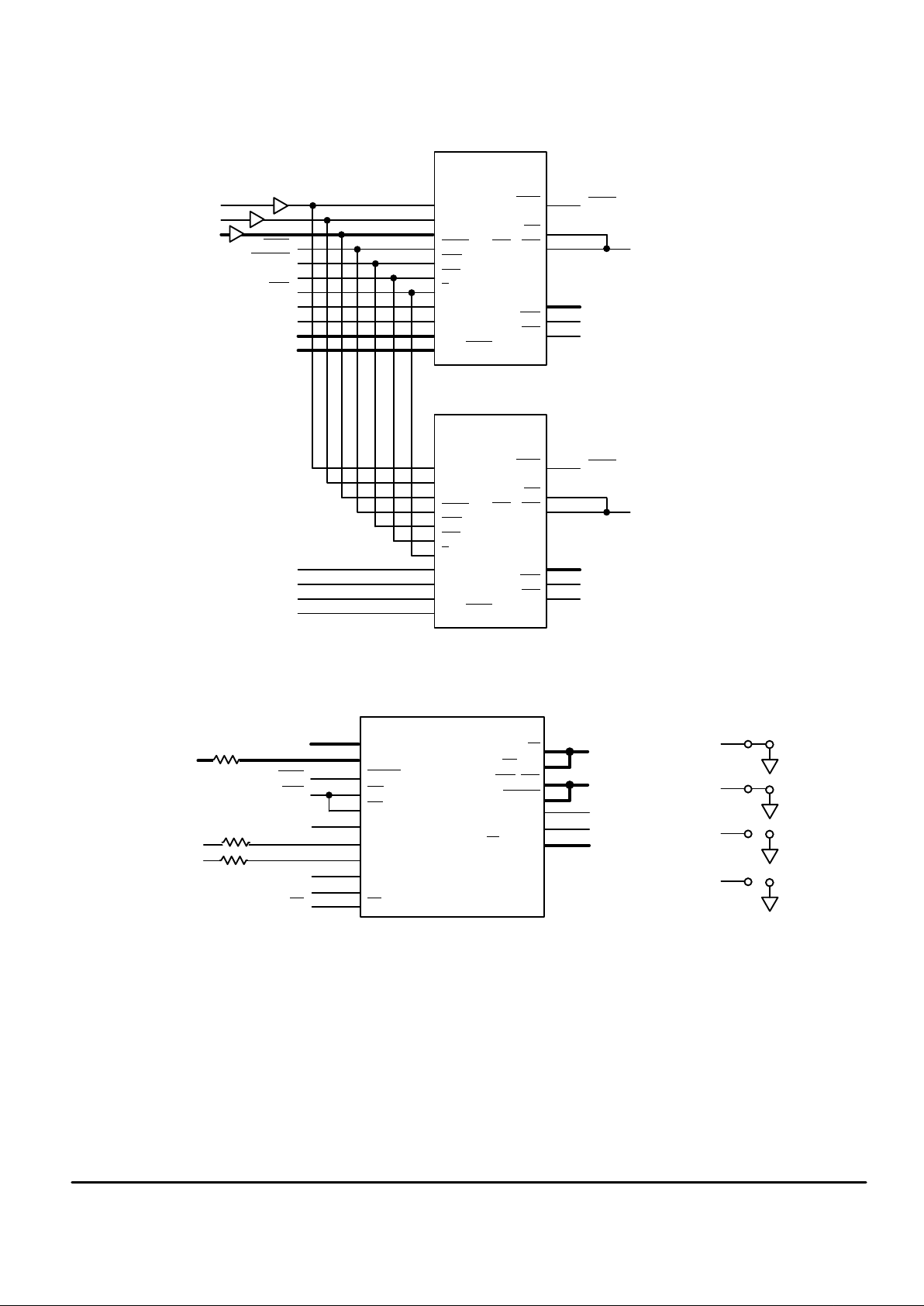
MPC2104P BLOCK DIAGRAM
32K x 32 SRAM
ADSC
ADV
SA1
ADS0
SA0
SA
A27
CWE0
A14 – A26
SBa – SBd
SW
SGW
PD3
PD2
PD1
PD0
J2
J0
J3
A14 – A26
A0 – A13
TCLR
TWE
CLK2
MATCH
VALIDIN
DIRTYIN
TG
TAG: 16K x 14 + V + D
A0 – A12
RESET
TDQ0 – TDQ13
TAH, TAG
, TAD
SFUNC, GS, A13
WS
WT
K
VALIDD
DIRTYD
GT
TT1, E1
E2, PWRDN
V
SS
VCC via 100
Ω
TA, VALIDQ
V
CCQ
V
DD
NC
MATCH
DIRTYOUT
DIRTYQ
J1
V
CC
V
CC
V
DD
ZZ
G
V
DD
SE1
K
CG0
DH0 – DH31
STANDBY
BURSTMODE
CLK0
SE3
LBO
DQa – DQd
SE2, ADSP
A28
CNTEN0
V
SS
V
SS
VDD via 100
Ω
V
DD
CLK1
V
SS
VDD via 100
Ω
V
DD
16244
32K x 32 SRAM
ADSC
ADV
SA1
SA0
SA
CWE1
SBa – SBd
SW
SGW
V
DD
ZZ
G
SE1
K
DL0 – DL31
STANDBY
BURSTMODE
SE3
LBO
DQa – DQd
SE2, ADSP
V
DD
22 Ω
22 Ω
22 Ω
Page 3

MPC2104P•MPC2105P
3
MOTOROLA FAST SRAM
MPC2105P BLOCK DIAGRAM
PD3
PD2
PD1
PD0
J2
J0
J3
A13 – A26
A0 – A12
TCLR
TWE
CLK2
MATCH
VALIDIN
DIRTYIN
TG
TAG: 16K x 14 + V + D
A0 – A13
RESET
TDQ0 – TDQ12
TAH, TAG, TAD
SFUNC, GS
WS
WT
K
VALIDD
DIRTYD
GT
TT1, E1
E2, PWRDN
V
SS
VCC via 100
Ω
TA, VALIDQ
V
CCQ
V
DD
NC
MATCH
DIRTYOUT
DIRTYQ
J1
V
CC
V
CC
TDQ13
V
SS
4.7K
Ω
64K x 32 SRAM
ADSC
ADV
SA1
ADS0
SA0
SA
A27
CWE0
A13 – A26
SBa – SBd
SW
SGW
V
DD
ZZ
G
V
DD
SE1
K
CG0
DH0 – DH31
STANDBY
BURSTMODE
CLK0
SE3
LBO
DQa – DQd
SE2, ADSP
A28
CNTEN0
V
SS
V
SS
VDD via 100
Ω
V
DD
CLK1
V
SS
VDD via 100
Ω
V
DD
16244
64K x 32 SRAM
ADSC
ADV
SA1
SA0
SA
CWE1
SBa – SBd
SW
SGW
V
DD
ZZ
G
SE1
K
DL0 – DL31
STANDBY
BURSTMODE
SE3
LBO
DQa – DQd
SE2, ADSP
V
DD
22Ω
22Ω
22Ω
Page 4

MPC2104P•MPC2105P
4
MOTOROLA FAST SRAM
PIN ASSIGNMENT 178–LEAD DIMM
Pin Name Pin Name Pin Name Pin Name Pin Name Pin Name Pin Name
1 V
SS
27 DH0 53 DL1 79 V
SS
105 DH14 131 DL17 157 A22
2 PD0/IDSCLK 28 NC 54 DL0 80 A7 106 DH13 132 NC 158 A20
3 PD2 29 V
SS
55 V
SS
81 A5 107 NC 133 DL15 159 V
SS
4 DH30 30 CLK1 56 CLK2 82 A3 108 DH10 134 DL13 160 A18
5 DH28 31 V
SS
57 V
SS
83 A0 109 DH8 135 V
SS
161 A16
6 DH26 32 DL28 58 NC 84 V
CC
110 NC 136 DL10 162 A15
7 DH24 33 DL26 59 CG0 85 TCLR 111 DH6 137 DL8 163 A14
8 V
DD
34 DL24 60 NC 86 MATCH 112 V
DD
138 CWE1 164 V
DD
9 NC 35 NC 61 V
DD
87 TG 113 DH4 139 DL6 165 A10
10 DH22 36 NC 62 NC 88 DIRTYIN 114 V
SS
140 V
DD
166 A8
11 DH20 37 DL22 63 RESER VED 89 V
SS
115 CLK0 141 DL5 167 A6
12 DH19 38 DL20 64 ADS0 90 V
SS
116 V
SS
142 DL2 168 V
SS
13 V
SS
39 DL18 65 NC 91 PD1/IDSDATA 117 DH1 143 V
SS
169 A4
14 DH17 40 DL16 66 A28 92 PD3 118 NC 144 NC 170 A2
15 NC 41 V
SS
67 A26 93 DH31 119 DL31 145 V
SS
171 A1
16 DH15 42 NC 68 A25 94 DH29 120 DL30 146 NC 172 BURSTMODE
17 DH12 43 DL14 69 A23 95 DH27 121 V
SS
147 V
SS
173 V
CC
18 NC 44 DL12 70 V
SS
96 DH25 122 DL29 148 CWE0 174 VALIDIN
19 DH11 45 DL11 71 A21 97 V
DD
123 DL27 149 NC 175 TWE
20 DH9 46 V
SS
72 A19 98 NC 124 DL25 150 V
DD
176 STANDBY
21 NC 47 DL9 73 A17 99 DH23 125 NC 151 NC 177 DIRTYOUT
22 DH7 48 NC 74 A13 100 DH21 126 NC 152 RESERVED 178 V
SS
23 V
DD
49 DL7 75 V
DD
101 DH18 127 DL23 153 CNTEN0
24 DH5 50 DL4 76 A12 102 V
SS
128 DL21 154 NC
25 DH3 51 V
DD
77 A11 103 DH16 129 DL19 155 A27
26 DH2 52 DL3 78 A9 104 NC 130 V
SS
156 A24
NOTE:VCC and VDD must be connected on all modules.
TOP VIEW – CASE TBD
1
42
43
89
90
131
132
178
65154
66155
Page 5

MPC2104P•MPC2105P
5
MOTOROLA FAST SRAM
PIN DESCRIPTIONS
Pin Locations Symbol
Type Description
66, 67, 68, 69, 71, 72, 73,
74, 76, 77, 78, 80, 81, 82,
83, 155, 156, 157, 158,
160, 161, 162, 163, 165,
166, 167, 169, 170, 171
A0 – A28 Input Address Inputs — (MSB:0, LSB:28).
64 ADS0 Input Data RAM Address Strobe.
172 BURSTMODE Input Burstmode. 0 = Linear, 1 = Interleaved.
59 CG0 Input Data RAM Output Enable.
30, 56, 115 CLK0 – CLK2 Input Clock Inputs — CLK2 is for Tag RAM, CLK0 and CLK1 are for Data RAMs only .
153 CNTEN0 Input Data RAM Count Enable.
138, 148 CWE0 – CWE1 Input Data RAM Write Enables — (MSB:0, LSB:1).
4, 5, 6, 7, 10, 11, 12, 14,
6, 17, 19, 20, 22, 24, 25,
26, 27, 93, 94, 95, 96, 99,
100, 101, 103, 105, 106,
108, 109, 111, 113, 117
DH0 – DH31 I/O High Data Bus — (MSB:0, LSB:31).
88 DIRTYIN Input Dirty input bit.
177 DIRTYOUT Output Dirty output bit.
32, 33, 34, 37, 38, 39, 40, 43,
44, 45, 47, 49, 50, 52, 53, 54,
119, 120, 122, 123, 124, 127,
128, 129, 131, 133, 134,
136, 137, 139, 141, 142
DL0 – DL31 I/O Low Data Bus — (MSB:0, LSB:31).
86 MATCH Output Tag RAM active high match indication.
2 PD0/IDSCLK Input Presence detect bit 0/EEPROM serial clock. (EEPROM option only).
91 PD1/IDSDATA I/O Presence detect bit 1/EEPROM serial data. (EEPROM option only).
3, 92 PD2, PD3 Output Presence detect bits.
63, 152 RESERVED Reserved pin.
176 STANDBY Input Standby pin. Reduces standby power consumption.
85 TCLR Input Tag RAM clear.
87 TG Input T ag RAM output enable.
175 TWE Input T ag RAM write enable.
174 VALIDIN Input T ag RAM valid bit.
84, 173 V
CC
Input + 5 V power supply. Must be connected.
8, 23, 51, 61, 75, 97,
112, 140, 150, 164
V
DD
Input + 3.3 V power supply. Must be connected.
1, 13, 29, 31, 41, 46, 55, 57,
70, 79, 89, 90, 102, 114,
116, 121, 130, 135, 143,
145, 147, 159, 168, 178
V
SS
Input Ground.
9, 15, 18, 21, 28, 35 – 36, 42,
48, 58, 60, 62, 65, 98, 104,
107, 110, 118, 125 – 126,
132, 144, 146, 149, 151, 154
NC — There is no connection to the module.
Page 6

MPC2104P•MPC2105P
6
MOTOROLA FAST SRAM
TRUTH TABLE (See Notes 1 through 4)
Next Cycle
Address
Used
Standby ADS0 CNTEN0 CG0
2
DHx/DLx CWEx
2
Deselect None 1 0 X X High–Z X
Begin Read External 0 0 X X High–Z 1
4
Continue Read Next X 1 0 1 High–Z 1
Continue Read Next X 1 0 0 DQ 1
Suspend Read Current X 1 1 1 High–Z 1
Suspend Read Current X 1 1 0 DQ 1
Begin Write External 0 0 X X High–Z 0
Continue Write Next X 1 0 X High–Z 0
Suspend Write Current X 1 1 X High–Z 0
NOTES:
1. X = Don’t Care. 1 = logic high. 0 = logic low.
2. CG0
is an asynchronous signal and is not sampled by the clock CLK0. CG0 drives the bus immediately (t
GLQX
) following CG0 going low.
3. On write cycles that follow read cycles, CG0
must be negated prior to the start of the write cycle to ensure proper write data setup times.
CG0
must also remain negated at the completion of the write cycle to ensure proper write data hold times.
4. This READ assumes the RAM was previously deselected.
ASYNCHRONOUS TRUTH TABLE
Operation CG0 I/O Status
Read L Data Out (DHx/DLx)
Read H High–Z
Write X High–Z
Deselected X High–Z
Sleep X High–Z
LINEAR BURST ADDRESS TABLE (Burst Mode = V
SS
)
1st Address (External) 2nd Address (Internal) 3rd Address (Internal) 4th Address (Internal)
X . . . X00 X . . . X01 X . . . X10 X . . . X11
X . . . X01 X . . . X10 X . . . X11 X . . . X00
X . . . X10 X . . . X11 X . . . X00 X . . . X01
X . . . X11 X . . . X00 X . . . X01 X . . . X10
INTERLEAVED BURST ADDRESS TABLE (Burst Mode = V
DD
)
1st Address (External)
2nd Address (Internal) 3rd Address (Internal) 4th Address (Internal)
X . . . X00 X . . . X01 X . . . X10 X . . . X11
X . . . X01 X . . . X00 X . . . X11 X . . . X10
X . . . X10 X . . . X11 X . . . X00 X . . . X01
X . . . X11 X . . . X10 X . . . X01 X . . . X00
Page 7

MPC2104P•MPC2105P
7
MOTOROLA FAST SRAM
ABSOLUTE MAXIMUM RATINGS (Voltages Referenced to V
SS
= 0 V)
Rating Symbol Value Unit
Power Supply Voltage Tag
Data RAM
V
CC
V
DD
– 0.5 to + 7.0
– 0.5 to + 4.6
V
Voltage Relative to V
SS Tag
Data RAM
Vin, V
out
– 0.5 to VCC + 0.5
– 0.5 to VDD + 0.5
V
Output Current (per I/O) Tag
Data RAM
I
out
± 20
± 30
mA
Power Dissipation P
D
3.86 W
Temperature Under Bias T
bias
– 10 to + 85 °C
Operating Temperature T
A
0 to +70 °C
Storage Temperature T
stg
– 55 to + 125 °C
NOTE: Permanent device damage may occur if ABSOLUTE MAXIMUM RATINGS are
exceeded. Functional operation should be restricted to RECOMMENDED OPERATING CONDITIONS. Exposure to higher than recommended voltages for
extended periods of time could affect device reliability.
DC OPERA TING CONDITIONS AND CHARACTERISTICS
(VCC = 5.0 V ± 5%, VDD = 3.3 V + 10%, – 5%, TA = 0 to + 70°C, Unless Otherwise Noted)
RECOMMENDED OPERATING CONDITIONS
(Voltages Referenced to VSS = 0 V)
Parameter Symbol Min Max Unit
Supply Voltage (Operating Voltage Range) V
CC
V
DD
4.75
3.135
5.25
3.60
V
Input High Voltage V
IH
2.2 VDD + 0.3** V
Input Low Voltage V
IL
– 0.5* 0.8 V
*VIL (min) = – 0.5 V dc; VIL (min) = – 2.0 V ac (pulse width ≤ 20 ns) for I ≤ 20.0 mA.
**VIH (max) = VDD + 0.3 V dc; VIH (max) = VDD + 2.0 V ac (pulse width ≤ 20 ns) for I ≤ 20.0 mA.
DC CHARACTERISTICS
Parameter Symbol Min Max Unit
Input Leakage Current (All Inputs, Vin = 0 to VDD) I
lkg(I)
— ± 1.0 µA
Output Leakage Current (CG = VIH, V
out
= 0 to VDD) I
lkg(O)
— ± 1.0 µA
TTL Output Low Voltage (IOL = + 8.0 mA) V
OL
— 0.4 V
TTL Output High Voltage (IOH = – 4.0 mA) V
OH
2.4 — V
POWER SUPPLY CURRENTS
Parameter Symbol Max Unit
AC Supply Current (CG = VIH, E = VIL, I
out
= 0 mA, All Inputs = VIL and VIH, MPC2104P
VIL = 0.0 V and VIH ≥ 3.0 V, Cycle T ime ≥ 20 ns) MPC2105P
I
DDA
410
700
mA
I
CCA
320 mA
AC Standby Current (E = VIH, I
out
= 0 mA, All Inputs = VIL or VIH MPC2104P
VIL = 0.0 V and VIH ≥ 3.0 V, Cycle T ime ≥ 20 ns) MPC2105P
I
SB1
(VDD) 210
240
mA
I
SB1
(VCC) 320 mA
CAPACITANCE (f = 1.0 MHz, dV = 3.0 V, T
A
= 25°C, Periodically Sampled Rather Than 100% Tested)
Parameter
Symbol Max Unit
Input Capacitance (A13 – A28)
(Data RAM Control Pins)
(CLK0 – CLK2)
(Tag Control Pins)
C
in
15
10
5
5
pF
Tag Output Capacitance (MATCH, DIRTYOUT) C
out
7 pF
Data RAM Input/Output Capacitance (DH0 – DH31, DL0 – DL31) C
I/O
8 pF
Tag Input/Output Capacitance (A0 – A11) C
I/O
7 pF
This device contains circuitry to protect the
inputs against damage due to high static voltages or electric fields; however, it is advised
that normal precautions be taken to avoid
application of any voltage higher than maximum rated voltages to this high–impedance
circuit.
This BiCMOS memory circuit has been
designed to meet the dc and ac specifications
shown in the tables, after thermal equilibrium
has been established.
This device contains circuitry that will ensure
the output devices are in High–Z at power up.
Page 8

MPC2104P•MPC2105P
8
MOTOROLA FAST SRAM
DATA RAMs AC OPERATING CONDITIONS AND CHARACTERISTICS
(VCC = 5.0 V ± 5%, VDD = 3.3 V + 10%, – 5%, TA = 0 to + 70°C, Unless Otherwise Noted)
Input Timing Measurement Reference Level 1.5 V. . . . . . . . . . . . . . .
Input Pulse Levels 0 to 3.0 V. . . . . . . . . . . . . . . . . . . . . . . . . . . . . . . . .
Input Rise/Fall Time 3 ns. . . . . . . . . . . . . . . . . . . . . . . . . . . . . . . . . . . .
Output Timing Reference Level 1.5 V. . . . . . . . . . . . . . . . . . . . . . . . . .
Output Load See Figure 1a Unless Otherwise Noted. . . . . . . . . . . . .
SYNCHRONOUS DATA RAMs READ/WRITE CYCLE TIMING (See Notes 1 and 2)
MPC2104P/5P
Parameter Symbol
Min Max
Unit Notes
Cycle Time t
KHKH
15 — ns
Clock Access Time t
KHQV
— 8 ns 3
Output Enable to Output Valid t
GLQV
— 6 ns
Clock High to Output Active t
KHQX1
0 — ns
Clock High to Output Change t
KHQX2
2 — ns
Output Enable to Output Active t
GLQX
0 — ns
Output Disable to Q High–Z t
GHQZ
— 8 ns
Clock High to Q High–Z t
KHQZ
2 8 ns
Clock High Pulse Width t
KHKL
5 — ns
Clock Low Pulse Width t
KLKH
5 — ns
Setup Times: Address
Address Status
Data In
Write
Address Advance
Chip Enable
t
AVKH
t
SVKH
t
DVKH
t
WVKH
t
BAVVKH
t
EVKH
2.5 — ns 4
Hold Times: Address
Address Status
Data In
Write
Address Advance
Chip Enable
t
KHAX
t
KHTSX
t
KHDX
t
KHWX
t
KHBAX
t
KHEX
0.5 — ns 4
NOTES:
1. All read and write cycle timings are referenced from CLK or CG0
.
2. CG
is a don’t care when CWEx is sampled low.
3. Maximum access times are guaranteed for all possible PowerPC external bus cycles.
4. This is a synchronous device. All addresses must meet the specified setup and hold times for
ALL
rising edges of CLK whenever ADS0
is low, and the chip is selected. All other synchronous inputs must meet the specified setup and hold times for
ALL
rising edges of
CLK when the chip is enabled. Chip enable must be valid at each rising edge of clock for the device (when ADS0
is low) to remain enabled.
Page 9

MPC2104P•MPC2105P
9
MOTOROLA FAST SRAM
BURST READSINGLE READ
ADS0
t
KHKL
t
KHKH
DQx
STANDBY
CLKx
CNTEN0
Q(A)
BURST WRITE
A14 – A26
AB
READ/WRITE CYCLES
t
KLKH
CD
CWEx
Q(B) Q(B+1)
t
KHQV
Q(B+2) Q(B+3)
D(C) D(C+1) D(C+2) D(C+3) D(D)
t
KHQV
DESELECTED
SINGLE
COE0
t
KHQX1
t
KHQX2
t
GHQZ
Q(n–1)
t
KHQZ
WRITE
Page 10

MPC2104P•MPC2105P
10
MOTOROLA FAST SRAM
T AG RAM
RESET FUNCTION TRUTH TABLE (See Notes 1 and 2)
TCLR
CLK TWE TAG0 – TAG11 DIRTYOUT MATCH Operation POWER
L L – H H High–Z L
(3)
L
(3)
Reset Status Active
L L – H L — — — Not Allowed —
NOTES:
1. H = VIH, L = VIL, X = don’t care, — = undefined.
2. TG
is X for this table.
3. These are output states.
READ FUNCTION TRUTH TABLE (See Notes 1, 2, and 3)
TG TWE CLK TAG0 – TAG11 VALIDIN DIRTYIN DIRTYOUT MATCH Operation
L H X D
out
— — D
out
D
out
Read Tag I/O
H X X High–Z — — — — Tag I/O Disable
WRITE FUNCTION TRUTH TABLE (See Notes 1 and 2)
TG TWE CLK TAG0 – TAG11 VALIDIN DIRTYIN DIRTYOUT MATCH Operation
H L L – H D
in
— — — L Write Tag I/O
L L L – H — — — — — Not Allowed
NOTES:
1. H = VIH, L = VIL, X = don’t care, — = undefined.
2. This table applies when RESET
and PWRDN are high.
3. D
out
in this case is the same as Din. The input data is written through to the outputs during the write operation.
MATCH FUNCTION TRUTH TABLE (See Notes 1 through 4)
TG
TWE TAG0 – TAG11 VALIDIN
(4)
DIRTYIN
(4)
MATCH Operation
X X — — — D
out
Selected
L H D
out
— — L Read Tag I/O
H L D
in
D
in
D
in
L Write Tag I/O, Status Bits
H H TAG
in
L — L Invalid Data — Dedicated Status Bits
H H TAG
in
H — H Match — Dedicated Status Bits
NOTES:
1. H = VIH, L = VIL, X = don’t care, — = undefined.
2. M = high if TAGin equals the memory contents at the address; M = low if TAGin does not equal the contents at that address.
3. PWRDN
and RESET are high for this table. GS and CLK are X.
4. This column represents the stored memory cell data for the given status bit at the selected address.
Page 11

MPC2104P•MPC2105P
11
MOTOROLA FAST SRAM
T AG RAM AC OPERATING CONDITIONS AND CHARACTERISTICS
(VCC = 5.0 V ± 5%, TA = 0 to + 70°C, Unless Otherwise Noted)
Input Timing Measurement Reference Level 1.5 V. . . . . . . . . . . . . . .
Input Pulse Levels 0 to 3.0 V. . . . . . . . . . . . . . . . . . . . . . . . . . . . . . . . .
Input Rise/Fall Time 3 ns. . . . . . . . . . . . . . . . . . . . . . . . . . . . . . . . . . . .
Output Timing Measurement Reference Level 1.5 V. . . . . . . . . . . . .
Output Load Figure 1a Unless Otherwise Noted. . . . . . . . . . . . . . . . .
TAG RAM READ CYCLE (See Notes 1 through 4)
Tag RAM
Parameter Symbol
Min Max
Unit
Clock Access Time t
KHQV
— 10 ns
Output Enable to Output Valid t
GLQV
— 8 ns
Output Enable to Output Active t
GLQX
0 — ns
Output Disable to Q High–Z t
GHQZ
1 6 ns
Status Bit Hold from Address Change t
AXSX
3 — ns
Address Access Time Status Bits t
AVSV
— 10 ns
Tag Bit Hold from Address Change t
AVQX
3 — ns
Address Access Time Tag Bits t
AVQV
— 12 ns
NOTES:
1. Setup and hold times, W (write) refers to TWE
.
2. A read cycle is defined by TWE
high. A write cycle is defined by TWE low.
3. Maximum access times are guaranteed for all possible MC68040 and PowerPC external bus cycles.
4. Tag reads are asynchronous.
TAG RAM WRITE CYCLE (See Notes 1 through 4)
Tag RAM
Parameter Symbol
Min Max
Unit
Cycle Time t
KHKH
15 — ns
Clock High Pulse Width t
KHKL
4.5 — ns
Clock Low Pulse Width t
KLKH
4.5 — ns
Clock High to Output Active t
KHQX
1.5 — ns
Setup Times Address
Write
t
AVKH
t
WVKH
3 — ns
Hold Times Address
Write
t
KHAX
t
KHWX
1.5 — ns
Status Output Hold t
KHSX
0 — ns
Clock High to Status Bits Valid t
KHSV
— 9 ns
NOTES:
1. Setup and hold times, W (write) refers to TWE
.
2. A read cycle is defined by TWE
high. A write cycle is defined by TWE low.
3. Maximum access times are guaranteed for all possible MC68040 and PowerPC external bus cycles.
4. Tag writes are synchronous.
Page 12

MPC2104P•MPC2105P
12
MOTOROLA FAST SRAM
TAG RAM WRITE AND READ CYCLES
CLK
A14 – A26
TWE
A0 – A13
TG
VALID VALID VALID
VALID INPUT VALID OUTPUT
VALID
OUTPUT
VALID
OUTPUT
VALID
VALID VALID
VALID VALID
t
AVKH
t
KHAX
STATUS WRITE TAG READ
TAG WRITE AFTER READ
t
WVKH
t
KHWX
t
WVKH
t
KHWX
t
KHSV
t
KHSX
t
WVKH
t
KHWX
t
KHQV
t
KHQX
t
AVSV
t
GHQZ
t
GLQX
t
AXSX
VALIDIN
DIRTYIN
DIRTYOUT
t
KHKL
t
KLKH
t
KHKH
t
GLQV
t
AVQV
t
AXQX
t
AVKH
t
KHAX
(SEE NOTE 1)
(SEE NOTE 1)
t
AVSV
t
AXSX
NOTES:
1. Transition is measured plus or minus 200 mV from steady state.
2. TCLR = High.
TAG READ
AFTER WRITE
(See Note 2)
Page 13

MPC2104P•MPC2105P
13
MOTOROLA FAST SRAM
TAG RAM MATCH CYCLE
Tag RAM
Parameter Symbol
Min Max
Unit
Clock High Write to MA TCH Invalid t
KHML
— 7 ns
Clock High Read to MATCH Valid t
KHMV
— 10 ns
Address Valid to MATCH Valid t
AVMV
— 10 ns
MATCH Valid Hold from Address Change t
AXMX
2 — ns
TG Low to MATCH Invalid t
GLML
— 7 ns
TG High to MATCH Valid t
GHMX
— 8 ns
TAG RAM RESET (TCLR) CYCLE
Tag RAM
Parameter Symbol
Min Max
Unit
TCLR Setup Time t
STC
4 — ns
TCLR Hold Time t
HTC
1 — ns
Status Bit Reset Time t
SRST
— 60 ns
Status Bit Hold from TCLR Low t
SHRS
2 — ns
TCLR Low to MATCH Invalid t
RSML
— 10 ns
TCLR High to MATCH Valid t
RSMV
— 100 ns
TCLR Low to TAG High–Z t
RSQZ
— 10 ns
TCLR High to TAG Active t
RSQX
— 100 ns
STANDBY Setup to TCLR Low t
PDSR
30 — ns
TCLR High to TWE Low t
RHWX
80 — ns
OUTPUT
Z0 = 50
Ω
50
Ω
VL = 1.5 V
(a) (b)
5 pF
+5 V
OUTPUT
255
Ω
480
Ω
TIMING LIMITS
The table of timing values shows either a
minimum or a maximum limit for each parameter. Input requirements are specified from
the external system point of view. Thus, address setup time is shown as a minimum
since the system must supply at least that
much time. On the other hand, responses
from the memory are specified from the device point of view. Thus, the access time is
shown as a maximum since the device never
provides data later than that time.
Figure 1. Test Loads
Page 14

MPC2104P•MPC2105P
14
MOTOROLA FAST SRAM
MATCH
CLK
A14 – A26*
TAG RAM MATCH CYCLE
VALID
MATCH VALID
VALID
t
AVMV
t
AXMX
t
KHWX
t
KHWX
t
WVKH
t
WVKH
t
WVKH
TWE
A0 – A13
TG
VALID ADDRESS
VALID MATCH DATA FROM: PROCESSOR PROCESSORTAG RAM
VALID
t
GLML
t
GLMX
t
KHML
t
KHMV
*Cache addresses used are: A14 – A26 for MPC2104P.
Page 15

MPC2104P•MPC2105P
15
MOTOROLA FAST SRAM
MATCH
CLK
t
HTC
TAG RAM TCLR FUNCTION
*Transition is measured plus or minus 200 mV from steady state.
t
RSQX
t
SRST
t
STC
t
WVKH
t
RSQZ*
t
RHWX
A0 – A13
TWE
DIRTYOUT
TCLR
VALID
t
SHRS
t
RSMV
ORDERING INFORMATION
(Order by Full Part Number)
2104P
MPC 2105P XX XX
Motorola Memory Prefix
Part Number
Full Part Numbers — MPC2104PDG66 MPC2104P = 256KB, synchronous pipelined
MPC2105PDG66 MPC2105P = 512KB, synchronous pipelined
Speed (66 = 66 MHz)
Package (DG = Gold Pad DIMM)
Page 16

MPC2104P•MPC2105P
16
MOTOROLA FAST SRAM
Motorola reserves the right to make changes without further notice to any products herein. Motorola makes no warranty , representation or guarantee regarding
the suitability of its products for any particular purpose, nor does Motorola assume any liability arising out of the application or use of any product or circuit, and
specifically disclaims any and all liability, including without limitation consequential or incidental damages. “T ypical” parameters which may be provided in Motorola
data sheets and/or specifications can and do vary in different applications and actual performance may vary over time. All operating parameters, including “Typicals”
must be validated for each customer application by customer’s technical experts. Motorola does not convey any license under its patent rights nor the rights of
others. Motorola products are not designed, intended, or authorized for use as components in systems intended for surgical implant into the body, or other
applications intended to support or sustain life, or for any other application in which the failure of the Motorola product could create a situation where personal injury
or death may occur. Should Buyer purchase or use Motorola products for any such unintended or unauthorized application, Buyer shall indemnify and hold Motorola
and its officers, employees, subsidiaries, affiliates, and distributors harmless against all claims, costs, damages, and expenses, and reasonable attorney fees
arising out of, directly or indirectly, any claim of personal injury or death associated with such unintended or unauthorized use, even if such claim alleges that
Motorola was negligent regarding the design or manufacture of the part. Motorola and are registered trademarks of Motorola, Inc. Motorola, Inc. is an Equal
Opportunity/Affirmative Action Employer.
Mfax is a trademark of Motorola, Inc.
How to reach us:
USA/EUROPE/ Locations Not Listed: Motorola Literature Distribution; JAP AN: Nippon Motorola Ltd.; Tatsumi–SPD–JLDC, 6F Seibu–Butsuryu–Center,
P .O. Box 5405, Denver, Colorado, 80217. 303–675–2140 or 1–800–441–2447 3–14–2 Tatsumi Koto–Ku, Tokyo 135, Japan. 81–3–3521–8315
Mfax: RMFAX0@email.sps.mot.com — TOUCHTONE 602–244–6609 ASIA/P ACIFIC: Motorola Semiconductors H.K. Ltd.; 8B Tai Ping Industrial Park,
INTERNET: http://Design–NET .com 51 Ting Kok Road, Tai Po, N.T., Hong Kong. 852–26629298
MPC2104P/D
◊
 Loading...