

Page 1
SEMICONDUCTOR TECHNICAL DATA
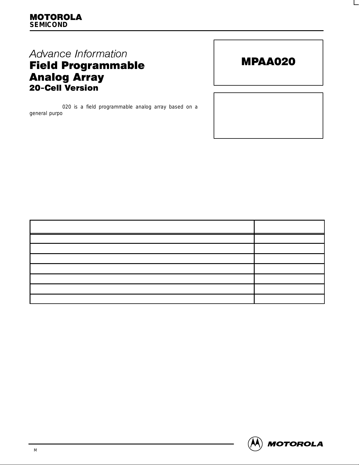
The MPAA020 is a field programmable analog array based on a
general purpose analog cell that may be configured, either alone or in
combinations, as any of a wide range of analog functions from simple
comparators to complex filters. These cells are arranged in a 4 x 5 array
with supporting circuitry to provide input/output signal buffering,
programmable reference voltages, cell to cell interconnections, etc. Each
cell’s function may be programmed to connect with any of the other cells
in the array. Unused cells are powered down individually to minimize power dissipation. Digital interface circuitry is provided to
write the analog circuit configuration data to on–chip SRAM in the same manner as Motorola’s digital FPGAs (serial & parallel
PROM, and microprocessor mode).
Analog circuit design is simplified with EasyAnalog Design Software, which handles bit level circuit configuration details,
allowing the user to do analog design using functional macros in an easy to use point–and–click graphical environment.
Table 1: Hardware Features
Feature Value
Number of Programmable Cells 20
Analog I/O Cells 13
Anti–aliasing/Smoothing Filtering Sallen–Key External RC
Additional Auxiliary Opamps 8
FIELD PROGRAMMABLE
ANALOG ARRAY
Internal Voltage Reference 8–Bit Programmable
Internal Clock Dividers 4 Independent 5–Bit Dividers
Package 160–Pin QFP
This document contains information on a new product. Specifications and information herein are subject to
change without notice.
4/97
Motorola, Inc. 1997
1
REV 0
Page 2
MPAA020
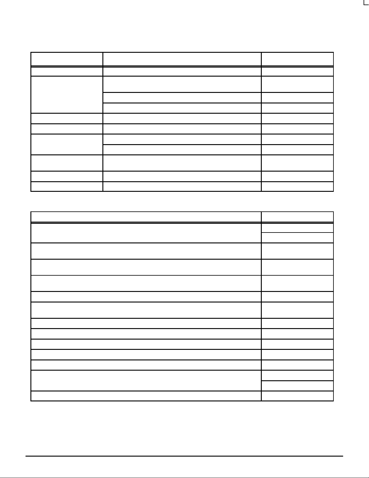
T able 2: EasyAnalog Design Software Macros
Macro Type Definable Parameters Range
Comparator Inverting/Non–inverting Reference level One/Two Input VMR ±2.5 volts
Filters Low Pass/ High Pass/Band Pass/Band Stop Single–Pole/Biquad/Cosine
Filter Pass Band Gain(s)
Q 0.5 to 255
Corner Frequencies Fclk/250 to Fclk/10
Gain Stages Inverting/Noninverting/Summing Offset compensating Gain Value ±(0.004 to 20)
Oscillators Square Wave/Sine Wave Frequency Fclk/1000 to Fclk/4
Rectifiers Full/Half Wave Inverting/Noninverting Gain ±(0.004 to 20)
Low Pass Pole Fclk/250 to Fclk/10
Signal Conditioning Sample–and–Hold
Track–and–Hold
Miscellaneous Differentiator / Integrators / Limiter 0.1 to 2.5 volts
Ramp Generator < 1 Hz to >20 kHz
±(0.004 to 20)
T able 3: Performance Specifications
Specification Typical Value
System Master Clock Frequency (clock) TBD
Internal Sampling Clock Rate 1 MHz (max)
Maximum Signal Frequency – Recommended
– Nyquist
200 kHz
500 kHz
Input Signal Range 0.5 to
Analog Output Drive 100 pF (max)
DC Offset < 10 mV
Harmonic Distortion – 1 kHz
– 200 kHz
Differential Non–Linearity < 0.15 LSB
Integral Non–Linearity < 0.24 LSB
Slew Rate 10 V/usec
Signal to Noise Ratio (SNR) > 60 dB
Power Supply Rejection Ratio (PSRR) TBD
Power Dissipation (max) 200 mW
Each cell individually selectable (10 mW/cell)
Operating Temperature Range –40 to + 85°C
(Vdd – 0.5)
1 kohm (min)
< 0.1%
< 0.5%
MOTOROLA ECLinPS and ECLinPS Lite
2
DL140 — Rev 3
Page 3
T able 4: Recommended Operating Conditions
Symbol Parameter Min Max Unit
MPAA020
AVDD, BVDD,
DVDD, SVDD
V
in
DC Supply Voltages 4.5 5.5 V
Input Voltage Analog
T able 5: Absolute Maximum Ratings
Symbol Parameter Min Max Unit
AVDD, BVDD,
DVDD, SVDD
V
in
T
A
T
stg
DC Supply Voltages –0.5 6.5 V
Input Voltage –0.5 VDD + 0.5 V
Operating Temperature Range –40 85 C
Storage Temperature –65 150 C
T able 6: Pin Descriptions
Pin Pin Name Type Description
1 por Digital Input Power On Reset
2 mode0 Digital Input Configuration mode control pins
3 mode1 Digital Input
Digital – VOH
Digital – VOL
0.5
2.0
0
VDD – 0.5
DVDD
0.8
V
4 mode2 Digital Input
5 mode3 Digital Input
6 cfg_clk Digital Input External Configuration Clock
7 DClk Digital Output Internal Configuration Clock
8 Data0 Digital Input
9 Data1 Digital Input
10 Data2 Digital Input
11 Data3 Digital Input
12 Data4 Digital Input
13 Data5 Digital Input
14 Data6 Digital Input
15 Data7 Digital Input
16 A0 Digital Output
17 A1 Digital Output
18 A2 Digital Output
19 A3 Digital Output
20 A4 Digital Output
Data Pins Used for Loading
Configuration Data
Address Pins Used for Loading
Configuration Data
DL140 — Rev 3
21 A5 Digital Output
22 A6 Digital Output
3 MOTOROLAECLinPS and ECLinPS Lite
Page 4

MPAA020
T able 6: Pin Descriptions
Pin DescriptionTypePin Name
23 A7 Digital Output
24 A8 Digital Output
25 A9 Digital Output
26 A10 Digital Output
27 A11 Digital Output
28 A12 Digital Output
29 A13 Digital Output
30 A14 Digital Output
31 A15 Digital Output
32 A16 Digital Output
33 A17 Digital Output
34 F1 (ERR, RD) Digital I/O Configuration Function Pins
35 F2 (MEMCE, WR) Digital I/O
36 F0 (BFR, CS) Digital I/O
37 F3 (PWRUP, RS) Digital I/O
38 F4 (END, BUSY) Digital I/O
39 opampDisable Digital Input Array opamp power–down
Address Pins Used for Loading
Configuration Data
40 reset Digital Input Chip RESET
41 No Connect Unused
42 No Connect Unused
43 No Connect Unused
44 No Connect Unused
45 No Connect Unused
46 No Connect Unused
47 No Connect Unused
48 No Connect Unused
49 ioLDX Analog Input Unbuffered Analog Input
50 ioLDY Analog Input Buffered Analog Input
51 ioLDZ Analog 0utput Buf fered Analog Output
52 No Connect
53 ioLDZ2 Analog Output Uncommitted Opamp Output
54 ioLDY2 Analog Input Uncommitted Opamp Input
55 No Connect Unused
56 ioLCY2 Analog Input Uncommitted Opamp Input
57 ioLCZ2 Analog Output Uncommitted Opamp Output
MOTOROLA ECLinPS and ECLinPS Lite
4
DL140 — Rev 3
Page 5

T able 6: Pin Descriptions
Pin DescriptionTypePin Name
58 No Connect
59 ioLCZ Analog Output Uncommitted Opamp Output
60 ioLCY Analog Input Buffered Analog Input
61 ioLCX Analog Input Unbuffered Analog Input
62 avdd Power Supply Analog VDD; 5 volts
63 avss Power Supply Analog VSS; 0 volts
64 svss Power Supply Substrate VSS; 0 volts
65 ioLBX Analog Input Unbuffered Analog Input
66 ioLBY Analog Input Buffered Analog Input
67 ioLBZ Analog 0utput Buf fered Analog Output
68 ioLBZ2 Analog Output Uncommitted Opamp Output
69 ioLBY2 Analog Input Uncommitted Opamp Input
MPAA020
70 No Connect Unused
71 ioLA Y2 Analog Input Uncommitted Opamp Input
72 ioLAZ2 Analog Output Uncommitted Opamp Output
73 ioLAZ Analog Output Uncommitted Opamp Output
74 ioLA Y Analog Input Buffered Analog Input
75 ioLAX Analog Input Unbuffered Analog Input
76 bvdd Power Supply VDD; 5 volts
77 bvss Power Supply VSS; 0 volts
78 No Connect Unused
79 No Connect Unused
80 No Connect Unused
81 vrefOut Analog Output Reference Voltage
82 vmr Analog Output Signal Ground; 2.5 volts
83 opamp_vmr Analog Output Signal Ground; 2.5 volts
84 cext External VMR capacitor
85 No Connect Unused
86 ioD5Z Analog Output Uncommitted Opamp Output
DL140 — Rev 3
87 ioD5Y Analog Input Buffered Analog Input
88 ioD5X Analog Input Unbuffered Analog Input
89 No Connect Unused
90 No Connect Unused
91 No Connect Unused
92 ioD4Z Analog Output Uncommitted Opamp Output
5 MOTOROLAECLinPS and ECLinPS Lite
Page 6

MPAA020
T able 6: Pin Descriptions
Pin DescriptionTypePin Name
93 ioD4Y Analog Input Buffered Analog Input
94 ioD4X Analog Input Unbuffered Analog Input
95 No Connect Unused
96 esd_vdd Power Supply VDD; 5 volts
97 esd_vss Power Supply VSS; 0 volts
98 No Connect Unused
99 No Connect Unused
100 No Connect Unused
101 ioD3Z Analog Output Uncommitted Opamp Output
102 ioD3Y Analog Input Buffered Analog Input
103 ioD3X Analog Input Unbuffered Analog Input
104 No Connect Unused
105 No Connect Unused
106 ioD2Z Analog Output Uncommitted Opamp Output
107 ioD2Y Analog Input Buffered Analog Input
108 ioD2X Analog Input Unbuffered Analog Input
109 No Connect Unused
110 No Connect Unused
111 No Connect Unused
112 ioD1Z Analog Output Uncommitted Opamp Output
113 ioD1Y Analog Input Buffered Analog Input
114 ioD1X Analog Input Unbuffered Analog Input
115 No Connect Unused
116 No Connect Unused
117 No Connect Unused
118 No Connect Unused
119 No Connect Unused
120 No Connect Unused
121 No Connect Unused
122 No Connect Unused
123 No Connect Unused
124 No Connect Unused
125 No Connect Unused
126* ioRAX Analog Input Unbuffered Analog Input
127 ioRA Y Analog Input Buffered Analog Input
MOTOROLA ECLinPS and ECLinPS Lite
6
DL140 — Rev 3
Page 7

T able 6: Pin Descriptions
Pin DescriptionTypePin Name
128 ioRAZ Analog 0utput Buffered Analog Output
129 ioRAZ2 Analog Output Uncommitted Opamp Output
130 ioRA Y2 Analog Input Uncommitted Opamp Input
131 No Connect Unused
132 ioRBY2 Analog Input Uncommitted Opamp Input
133 ioRBZ2 Analog Output Uncommitted Opamp Output
134 ioRBZ Analog 0utput Buffered Analog Output
135 ioRBY Analog Input Buffered Analog Input
136 ioRBX Analog Input Unbuffered Analog Input
137 cfg_vdd Power Supply Digital VDD; 5 volts
138 svss Power Supply Substrate VSS; 0 volts
139 svdd Power Supply Substrate VDD; 5 volts
MPAA020
140 clock Digital Input System Master Clock
141 No Connect Unused
142 ioRCX Analog Input Unbuffered Analog Input
143 ioRCY Analog Input Buffered Analog Input
144 ioRCZ Analog 0utput Buffered Analog Output
145 ioRCZ2 Analog Output Uncommitted Opamp Output
146 ioRCY2 Analog Input Uncommitted Opamp Input
147 No Connect Unused
148 ioRDY2 Analog Input Uncommitted Opamp Input
149 ioRDZ2 Analog Output Uncommitted Opamp Output
150 cfg_vss Power Supply Digital config logic VSS; 0 volts
151 No Connect Unused
152 ioRDZ Analog 0utput Buffered Analog Output
153 ioRDY Analog Input Buffered Analog Input
154 ioRDX Analog Input Unbuffered Analog Input
155 No Connect Unused
156 No Connect Unused
DL140 — Rev 3
157 No Connect Unused
158 No Connect Unused
159 No Connect Unused
160 No Connect Unused
7 MOTOROLAECLinPS and ECLinPS Lite
Page 8

MPAA020
Motorola reserves the right to make changes without further notice to any products herein. Motorola makes no warranty , representation or guarantee regarding
the suitability of its products for any particular purpose, nor does Motorola assume any liability arising out of the application or use of any product or circuit, and
specifically disclaims any and all liability, including without limitation consequential or incidental damages. “T ypical” parameters which may be provided in Motorola
data sheets and/or specifications can and do vary in different applications and actual performance may vary over time. All operating parameters, including “Typicals”
must be validated for each customer application by customer’s technical experts. Motorola does not convey any license under its patent rights nor the rights of
others. Motorola products are not designed, intended, or authorized for use as components in systems intended for surgical implant into the body, or other
applications intended to support or sustain life, or for any other application in which the failure of the Motorola product could create a situation where personal injury
or death may occur. Should Buyer purchase or use Motorola products for any such unintended or unauthorized application, Buyer shall indemnify and hold Motorola
and its officers, employees, subsidiaries, affiliates, and distributors harmless against all claims, costs, damages, and expenses, and reasonable attorney fees
arising out of, directly or indirectly, any claim of personal injury or death associated with such unintended or unauthorized use, even if such claim alleges that
Motorola was negligent regarding the design or manufacture of the part. Motorola and are registered trademarks of Motorola, Inc. Motorola, Inc. is an Equal
Opportunity/Affirmative Action Employer.
How to reach us:
USA/EUROPE/Locations Not Listed: Motorola Literature Distribution; JAPAN: Nippon Motorola Ltd.; Tatsumi–SPD–JLDC, 6F Seibu–Butsuryu–Center,
P.O. Box 5405, Denver, Colorado 80217. 303–675–2140 or 1–800–441–2447 3–14–2 T atsumi Koto–Ku, Tokyo 135, Japan. 81–3–3521–8315
Mfax: RMFAX0@email.sps.mot.com – TOUCHTONE 602–244–6609 ASIA/PACIFIC: Motorola Semiconductors H.K. Ltd.; 8B Tai Ping Industrial Park,
INTERNET: http://www.mot.com/SPS/
– US & Canada ONLY 1–800–774–1848 51 Ting Kok Road, Tai Po, N.T., Hong Kong. 852–26629298
◊
MOTOROLA ECLinPS and ECLinPS Lite
8
Mfax is a trademark of Motorola, Inc.
MPAA020/D
DL140 — Rev 3
 Loading...