

Page 1
MP7533
15 V CMOS
Multiplying10-Bit
Digital-to-Analog Converter
FEATURES
• 10-Bit Resolution
• Non-Linearity: 1/2 LSB to 2 LSB
• Nonlinearity Tempco: 0.2 ppm of FSR/°C, Max.
• Low Power Dissipation: 20 mW
• Current Settling Time: 500 ns
• Feedthrough Error: 1 mV p-p @ 10 kHz, Max.
• TTL/CMOS Compatible
• Latch-Up Free
• Improved Replacement for AD7533
GENERAL DESCRIPTION
The MP7533 is a low cost, 10-bit multiplying Digital-to-Analog
Converter. This device uses EXAR’s patented advanced thin
film resistor and CMOS technologies, providing up to 10-bit accuracies with TTL/CMOS compatibility.
BENEFITS
• Accurate Converter at Low Cost
• Can be used in Reverse Mode (V oltage Out)
• Flexible Design
APPLICATIONS
• Digital/Analog Multiplication
• Character Generation
• Programmable Power Supplies
• Gain Controlled Circuits
Pin and functional equivalent to the industry standard
MP7520, the MP7533 is recommended as a lower cost alternative for old MP7520 sockets or new 10-bit DAC designs.
The MP7533 applications include: digital-to-analog multiplication, CRT character generation, programmable power supplies, digitally controlled gain circuits, etc.
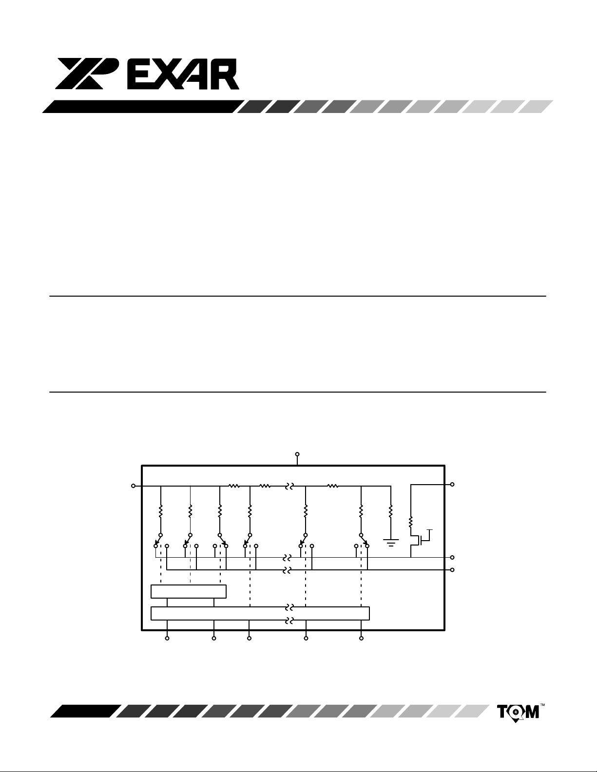
SIMPLIFIED BLOCK DIAGRAM
V
REF
4R
4R 4R 4R 4R 4R 4R
2 to 3 Decoder
Switch Drivers & Switches
BIT 1
MSB LSB
3 Segment D/A Converter with Termination to DGND
Logical “1” at Digital Input Steers Current to I
V
DD
2R2R
2R
BIT 10
OUT1
R
R = 10k
R
FB
I
OUT1
I
OUT2
Rev. 2.00
1
Page 2
MP7533
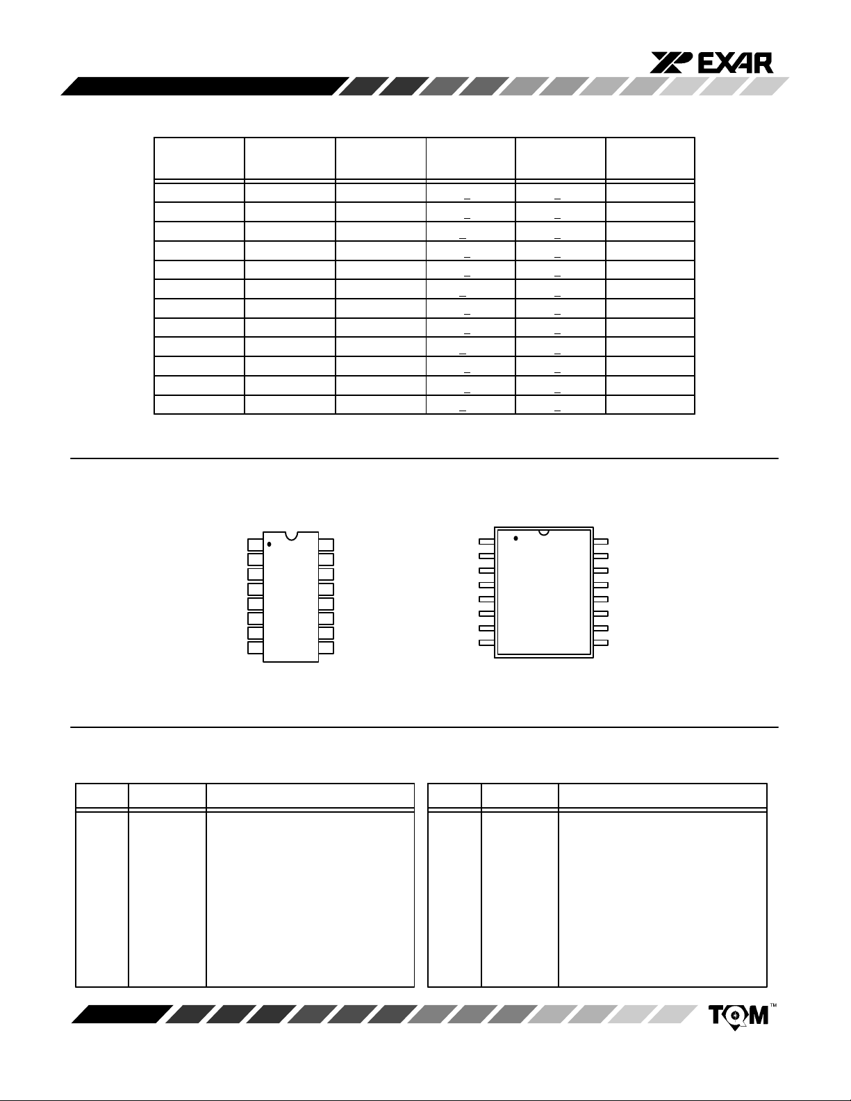
ORDERING INFORMATION
Package
Type
Plastic Dip MP7533JN
Plastic Dip MP7533KN
Plastic Dip MP7533LN
SOIC MP7533JS
SOIC MP7533KS
SOIC MP7533LS
Ceramic Dip MP7533AD
Ceramic Dip MP7533BD
Ceramic Dip MP7533CD
Ceramic Dip MP7533SD*
Ceramic Dip MP7533TD*
Ceramic Dip MP7533UD*
*Contact factory for non-compliant military processing
PIN CONFIGURATIONS
I
OUT1
I
OUT2
GND
(MSB) BIT 1
BIT 2
BIT 3
BIT 4
BIT 5
Temperature
Range
–40 to +85
–40 to +85
–40 to +85
–40 to +85
–40 to +85
–40 to +85
–40 to +85
–40 to +85
–40 to +85°C
–55 to +125
–55 to +125
–55 to +125°C
°C
°C
°C
°C
°C
°C
°C
°C
°C
°C
Part No.
INL
(LSB)
2
+
+1
1/2
+
2
+
1
+
+
1/2
+2
1
+
+1/2
+
2
+
1
+1/2
See Packaging Section for Package Dimensions
1
2
3
4
5
6
7
8
16
R
15
V
V
14
BIT 10 (LSB)
13
12
BIT 9
BIT 8
11
BIT 7
10
BIT 6
9
FB
REF
DD
1
2
3
4
5
6
7
Pin Out
at Left
(LSB)
See
DNL
1
+
+1
1
+
1
+
1
+
+
1
1
+
1
+
+1
+
1
+
1
+1
Gain Error
(% FSR)
1.5
1.5
1.5
1.5
1.5
1.5
1.5
1.5
1.5
1.5
1.5
1.5
16
15
14
13
12
11
10
98
16 Pin CDIP, PDIP (0.300”)
D16, N16
PIN OUT DEFINITIONS
PIN NO. NAME DESCRIPTION
1I
2I
OUT1
OUT2
3 GND Ground
4 BIT 1 Data Input Bit 1 (MSB)
5 BIT 2 Data Input Bit 2
6 BIT 3 Data Input Bit 3
7 BIT 4 Data Input Bit 4
8 BIT 5 Data Input Bit 5
Rev. 2.00
Current Output 1
Current Output 2
16 Pin SOIC (Jedec, 0.300”)
S16
PIN NO. NAME DESCRIPTION
9 BIT 6 Data Input Bit 6
10 BIT 7 Data Input Bit 7
11 BIT 8 Data Input Bit 8
12 BIT 9 Data Input Bit 9
13 BIT 10 Data Input Bit 10 (LSB)
Positive Power Supply
Reference Input Voltage
Internal Feedback Resistor
2
14 V
15 V
16 R
DD
REF
FB
Page 3
ELECTRICAL CHARACTERISTICS
(VDD = + 15 V, V
= +10 V unless otherwise noted)
REF
MP7533
25°C
Tmin to Tmax
Parameter Symbol Min Typ Max Min Max Units Test Conditions/Comments
STATIC PERFORMANCE
1
FSR = Full Scale Range
Resolution (All Grades) N 10 10 Bits
Integral Non-Linearity INL LSB Best Fit Straight Line Spec.
(Relative Accuracy) (Max INL – Min INL) / 2
A, S, J +
B, T, K +
C, U, L +
2+2
1+1
1/2 +1/2
Differential Non-Linearity DNL LSB
A, S, J +
B, T, K +
C, U, L +
Gain Error GE +
Gain Temperature Coefficient
2
TC
GE
Power Supply Rejection Ratio PSRR +
Output Leakage Current I
OUT
0.4 +1.5 +1.5 % FSR Using Internal R
30 +50 +50 ppm/% |∆Gain/∆VDD| ∆VDD = + 5%
1+1
1+1
1+1
FB
+2 ppm/°C ∆Gain/∆Temperature
+50 +200 nA
REFERENCE INPUT
Input Resistance R
DIGITAL INPUTS
3
IN
5 10 20 5 20 kΩ
Logical “1” Voltage V
Logical “0” Voltage V
Input Leakage Current I
LKG
3.0 2.4 3.0 V
IH
IL
0.8 0.8 V
+1+1µA
ANALOG OUTPUTS
Output Capacitance
POWER SUPPLY
Functional Voltage Range
Supply Current I
2
C
OUT1
C
OUT1
C
OUT2
C
OUT2
4
2
V
DD
DD
4.5 15 4.5 15 V
52 pF DAC Inputs all 1’s
26 pF DAC Inputs all 0’s
13 pF DAC Inputs all 1’s
45 pF DAC Inputs all 0’s
2 2 mA All digital inputs = 0 or all = 5 V
Total Dissipation 20 mW
NOTES:
1
Full Scale Range (FSR) is 10V for unipolar mode.
2
Guaranteed but not production tested
3
Digital Input levels should not go below ground or exceed the positive supply voltage, otherwise damage may occur.
4
Specified values guarantee functionality. Refer to other parameters for accuracy.
Specifications are subject to change without notice
Rev. 2.00
3
Page 4

MP7533
ABSOLUTE MAXIMUM RATINGS (TA = +25°C unless otherwise noted)
VDD to GND +17 V. . . . . . . . . . . . . . . . . . . . . . . . . . . . . . . . . . .
Digital Input Voltage to GND GND –0.5 to V
, I
I
OUT1
V
REF
V
RFB
NOTES:
1
2
to GND –0.5 to VDD +0.5 V. . . . . . . . . . . . . . . .
OUT2
to GND +25 V. . . . . . . . . . . . . . . . . . . . . . . . . . . . . . . . . .
to GND +25 V. . . . . . . . . . . . . . . . . . . . . . . . . . . . . . . . . .
Stresses above those listed under “Absolute Maximum Ratings” may cause permanent damage to the device. This is a
stress rating only and functional operation at or above this specification is not implied. Exposure to maximum rating
conditions for extended periods may affect device reliability.
Any input pin which can see a value outside the absolute maximum ratings should be protected by Schottky diode clamps
(HP5082-2835) from input pin to the supplies.
transients outside the supplies of less than 20mA for less than 100
+0.5 V. . . .
DD
All inputs have protection diodes
Storage Temperature –65
Lead Temperature (Soldering, 10 seconds) +300
Package Power Dissipation Rating to 75°C
CDIP, PDIP, SOIC, PLCC 700mW. . . . . . . . . . . . . . . . . .
Derates above 75
µs.
1, 2
°C to +150°C. . . . . . . . . . . . . . . . .
°C 10mW/°C. . . . . . . . . . . . . . . . . . . . .
which will protect the device from short
APPLICATION NOTES
Refer to Section 8 for Applications Information
°C. . . . . .
Rev. 2.00
4
Page 5

16 LEAD CERAMIC DUAL-IN-LINE
(300 MIL CDIP)
D16
MP7533
S
1
See
Note 1
Base
Plane
Seating
Plane
INCHES MILLIMETERS
SYMBOL MIN MAX MIN MAX NOTES
A –– 0.200 –– 5.08 ––
b 0.014 0.023 0.356 0.584 ––
b 0.038 0.065 0.965 1.65 2
1
c 0.008 0.015 0.203 0.381 ––
D –– 0.840 –– 21.34 4
E 0.220 0.310 5.59 7.87 4
E 0.290 0.320 7.37 8.13 7
1
e 0.100 BSC 2.54 BSC 5
L 0.125 0.200 3.18 5.08 ––
L 0.150 –– 3.81 –– ––
1
Q 0.015 0.060 0.381 1.52 3
S –– 0.080 –– 2.03 6
S 0.005 –– 0.13 –– 6
1
L
16
18
Q
e
b
S
9
D
b
1
α 0° 15° 0° 15° ––
E
1
E
A
L
1
α
NOTES
1. Index area; a notch or a lead one identification mark
is located adjacent to lead one and is within the
shaded area shown.
2. The minimum limit for dimension b
(0.58 mm) for all four corner leads only.
3. Dimension Q shall be measured from the seating
plane to the base plane.
4. This dimension allows for off-center lid, meniscus and
glass overrun.
5. The basic lead spacing is 0.100 inch (2.54 mm) between centerlines.
6. Applies to all four corners.
7. This is measured to outside of lead, not center.
c
may be 0.023
1
Rev. 2.00
5
Page 6

MP7533
16 LEAD PLASTIC DUAL-IN-LINE
(300 MIL PDIP)
N16
S
Seating
Plane
16
1
Q
1
A
L
B
SYMBOL MIN MAX MIN MAX
A –– 0.200 –– 5.08
A
1
B 0.014 0.023 0.356 0.584
B
(1) 0.038 0.065 0.965 1.65
1
C 0.008 0.015 0.203 0.381
D 0.745 0.785 18.92 19.94
E 0.295 0.325 7.49 8.26
E
1
e 0.100 BSC 2.54 BSC
L 0.115 0.150 2.92 3.81
D
e
INCHES
0.015 –– 0.38 ––
0.220 0.310 5.59 7.87
9
8
B
1
α 0° 15° 0° 15°
Q
1
S 0.020 0.080 0.51 2.03
0.055 0.070 1.40 1.78
E
1
A
1
MILLIMETERS
E
C
α
Rev. 2.00
Note: (1) The minimum limit for dimensions B1 may be 0.023”
(0.58 mm) for all four corner leads only.
6
Page 7

16 LEAD SMALL OUTLINE
(300 MIL JEDEC SOIC)
D
16 9
MP7533
S16
E H
8
h x 45°
Seating
Plane
C
e
SYMBOL MIN MAX MIN MAX
A 0.097 0.104 2.46 2.64
A
1
B 0.014 0.019 0.356 0.482
C 0.0091 0.0125 0.231 0.318
D 0.402 0.412 10.21 10.46
E 0.292 0.299 7.42 7.59
e 0.050 BSC 1.27 BSC
H 0.400 0.410 10.16 10.41
h 0.010 0.016 0.254 0.406
L 0.016 0.035 0.406 0.889
B
A
1
INCHES MILLIMETERS
0.0050 0.0115 0.127 0.292
α 0° 8° 0° 8°
A
α
L
Rev. 2.00
7
Page 8

MP7533
NOTICE
EXAR Corporation reserves the right to make changes to the products contained in this publication in order to improve design, performance or reliability . EXAR Corporation assumes no responsibility for the use of any circuits described herein, conveys no license under any patent or other right, and makes no representation that the circuits are
free of patent infringement. Charts and schedules contains here in are only for illustration purposes and may vary
depending upon a user’s specific application. While the information in this publication has been carefully checked;
no responsibility, however, is assumed for inaccuracies.
EXAR Corporation does not recommend the use of any of its products in life support applications where the failure or
malfunction of the product can reasonably be expected to cause failure of the life support system or to significantly
affect its safety or effectiveness. Products are not authorized for use in such applications unless EXAR Corporation
receives, in writing, assurances to its satisfaction that: (a) the risk of injury or damage has been minimized; (b) the
user assumes all such risks; (c) potential liability of EXAR Corporation is adequately protected under the circumstances.
Copyright EXAR Corporation
Datasheet April 1995
Reproduction, in part or whole, without the prior written consent of EXAR Corporation is prohibited.
Rev. 2.00
8
 Loading...