

Page 1
MP03 XX 260 Series
MP03 XX 260 Series
Dual Diode Modules
Replaces December 1998 version, DS5104-2.0 DS5104-3.0 January 2000
FEATURES
■ Dual Device Module
■ Electrically Isolated Package
■ Pressure Contact Construction
■ International Standard Footprint
■ Alumina (non-toxic) Isolation Medium
APPLICATIONS
■ Rectifier Bridges
■ DC Power Bridges
■ Plating Rectifiers
■ Traction Systems
VOLTAGE RATINGS
Type
Number
Repetitive
Peak
Voltages
V
RRM
MP03/260-16
MP03/260-14
MP03/260-12
MP03/260-10
Lower voltage grades available. For full description of part
numbers see "Ordering instructions" on page 3.
1600
1400
1200
1000
Conditions
Tvj = 150oC
IRM = 30mA
V
= V
RSM
RRM
+ 100V
KEY PARAMETERS
V
RRM
I
FSM
I
(per arm) 267A
F(AV)
V
isol
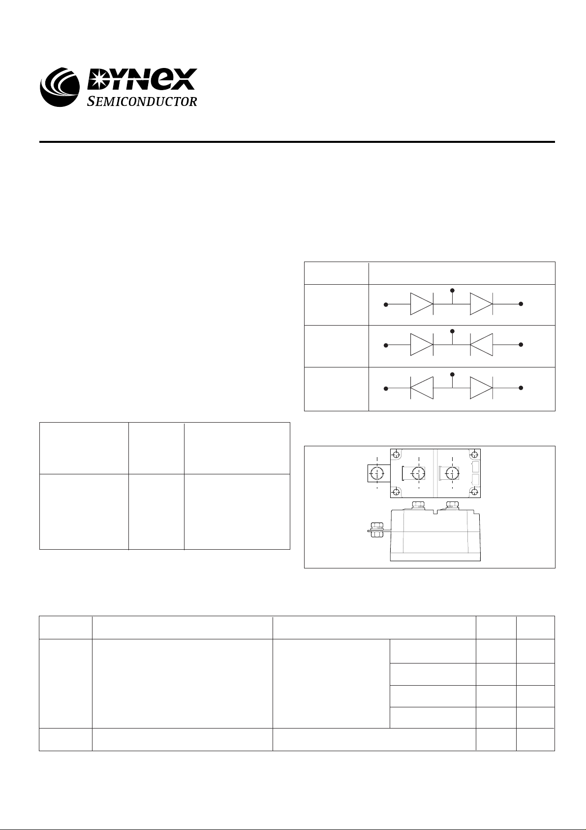
CIRCUIT OPTIONS
Code
HB
G
GN
Circuit
PACKAGE OUTLINE
Module outline type code: MP03.
See Package Details for further information.
1600V
8100A
2500V
CURRENT RATINGS - PER ARM
Symbol
I
F(AV)
F(RMS)
Mean forward current
RMS value A420
Parameter Units
Conditions
Halfwave, resistive load
T
= 75oCI
case
T
case
T
case
T
heatsink
T
heatsink
= 75oC
= 85oC
= 75oC
= 85oC
Max.
267
240
235
A
A
A
A211
1/9
Page 2

MP03 XX 260 Series
SURGE RATINGS - PER ARM
Symbol Parameter
I
I2t
FSM
Surge (non-repetitive) forward current
I2t for fusing
THERMAL & MECHANICAL RATINGS
Symbol
R
th(j-c)
R
th(c-hs)
vj
T
sto
Thermal resistance - junction to case
per Diode
Thermal resistance - case to heatsink
per Diode
Virtual junction temperatureT
Storage temperature range
Parameter
Conditions Max.
VR = 0
10ms half sine;
Tj = 150˚C
VR = 50% V
VR = 0
10ms half sine;
Tj = 150˚C
VR = 50% V
Conditions
dc
halfwave
3 phase
Mounting torque = 5Nm
with mounting compound
RRM
RRM
8100
6500
328000
211000
Max.
0.21
0.22
0.23
0.05
150
-40 to 150
Units
A
A
A2s
A2s
Units
o
C/W
o
C/W
o
C/W
o
C/W
o
C
o
C
V
isol
Isolation voltage
CHARACTERISTICS
Symbol
V
FM
I
RM
V
TO
r
T
Forward voltage
Peak reverse current At V
Threshold voltage V0.84At Tvj = 150oC
On-state slope resistance
Parameter
Commoned terminals to base plate
AC RMS, 1min, 50Hz
Conditions
At 600A, T
RRM
= 25oC
case
, Tj = 150oC
2.5
Max.
1.3
30
kV
Units
V
mA
mΩ0.667At Tvj = 150oC
2/9
Page 3

MP03 XX 260 Series
ORDERING INSTRUCTIONS
Part number is made up as follows:
MP03 HB 260 - 16
MP = Pressure contact module
03 = Outline type
HB = Circuit configuration code (see "circuit options" - front page)
260 = Nominal average current rating at T
16 = V
RRM
/100
Examples:
MP03 HB260-10
MP03 G260-14
MP023GN260-12
Note: Preferred type is HB configuration. G & GN types are available for specific applications, only when requested.
MOUNTING RECOMMENDATIONS
= 75oC
case
Adequate heatsinking is required to maintain the base
temperature at 75oC if full rated current is to be achieved.
Power dissipation may be calculated by use of VTO and r
information in accordance with standard formulae. We can
provide assistance with calculations or choice of heatsink
if required.
The heatsink surface must be smooth and flat; a surface
finish of N6 (32µin) and a flatness within 0.05mm (0.002")
are recommended.
Immediately prior to mounting, the heatsink surface should
be lightly scrubbed with fine emery, Scotch Brite or a mild
chemical etchant and then cleaned with a solvent to
remove oxide build up and foreign material. Care should
be taken to ensure no foreign particles remain.
An even coating of thermal compound (eg. Unial) should be
applied to both the heatsink and module mounting surfaces.
This should ideally be 0.05mm (0.002") per surface to
T
ensure optimum thermal performance.
After application of thermal compound, place the module
squarely over the mounting holes, (or 'T' slots) in the
heatsink. Using a torque wrench, slowly tighten the
recommended fixing bolts at each end, rotating each in turn
no more than 1/4 of a revolution at a time. Continue until the
required torque of 5Nm (44lb.ins) is reached at both ends.
It is not acceptable to fully tighten one fixing bolt before
starting to tighten the others. Such action may DAMAGE the
module.
3/9
Page 4
MP03 XX 260 Series
CURVES
2500
2000
- (A)
F
1500
1000
Instantaneous forward current I
500
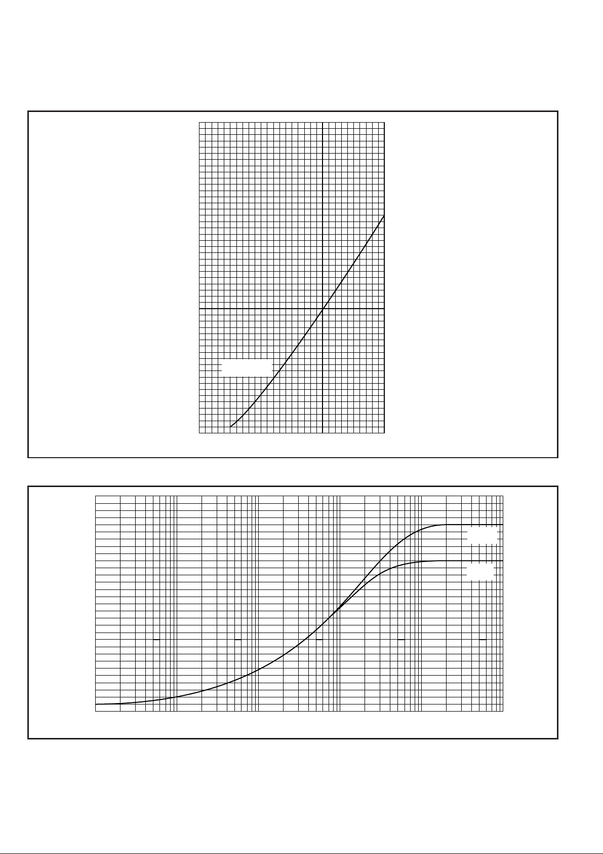
Fig. 1 Maximum (limit) forward characteristics (Per diode)
0.3
0.2
0.1
Thermal Impedance - (˚C/W)
Tj = 150˚C
0
0.5 1.0 1.5 2.0
Instantaneous forward voltage IF - (V)
R
R
th(j-hs)
th(j-c)
4/9
0
0.001 0.010 0.100 1.0 10 100
Fig. 2 Transient thermal impedance (DC) - (Per diode)
Time - (s)
Page 5
15000
MP03 XX 260 Series
12500
I2t
10000
7500
5000
Peak half sine wave forward current - (A)
2500
0
11012355010 20 30
ms cycles at 50Hz
Duration
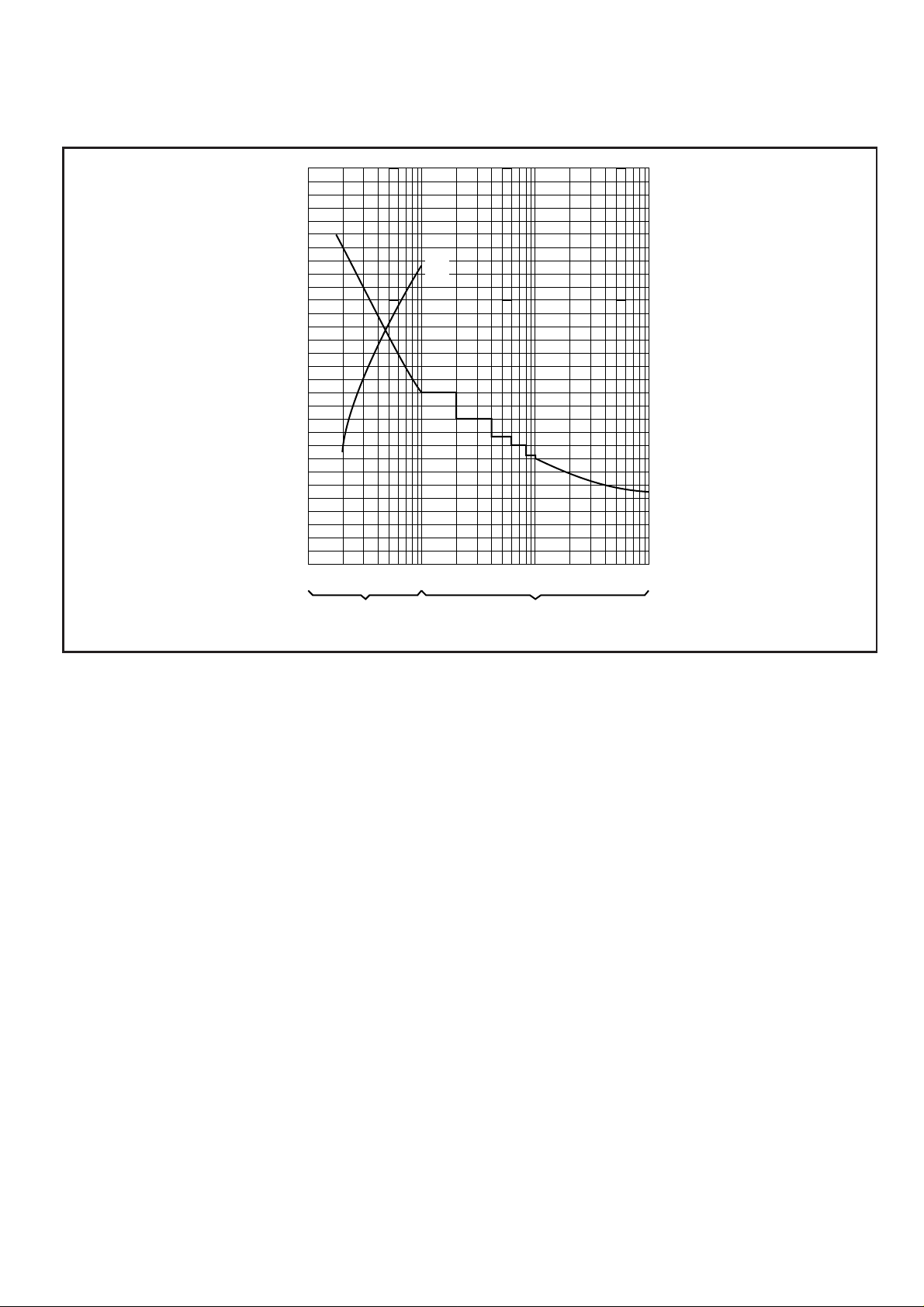
Fig. 3 Surge (non-repetitive) forward current vs time (with 0% V
RRM
, T
22
20
I
2
t value - A
18
16
2
s x 10
14
4
12
10
= 150˚C)
case
5/9
Page 6
MP03 XX 260 Series
500
450
400
350
300
d.c.
180˚ Rectangular
180˚ Sine
120˚ Rectangular
250
60˚ Rectangular
200
150
On-state power loss per device - (W)
100
50
0
0 50 100 150 200 250
Mean forward current - (A)
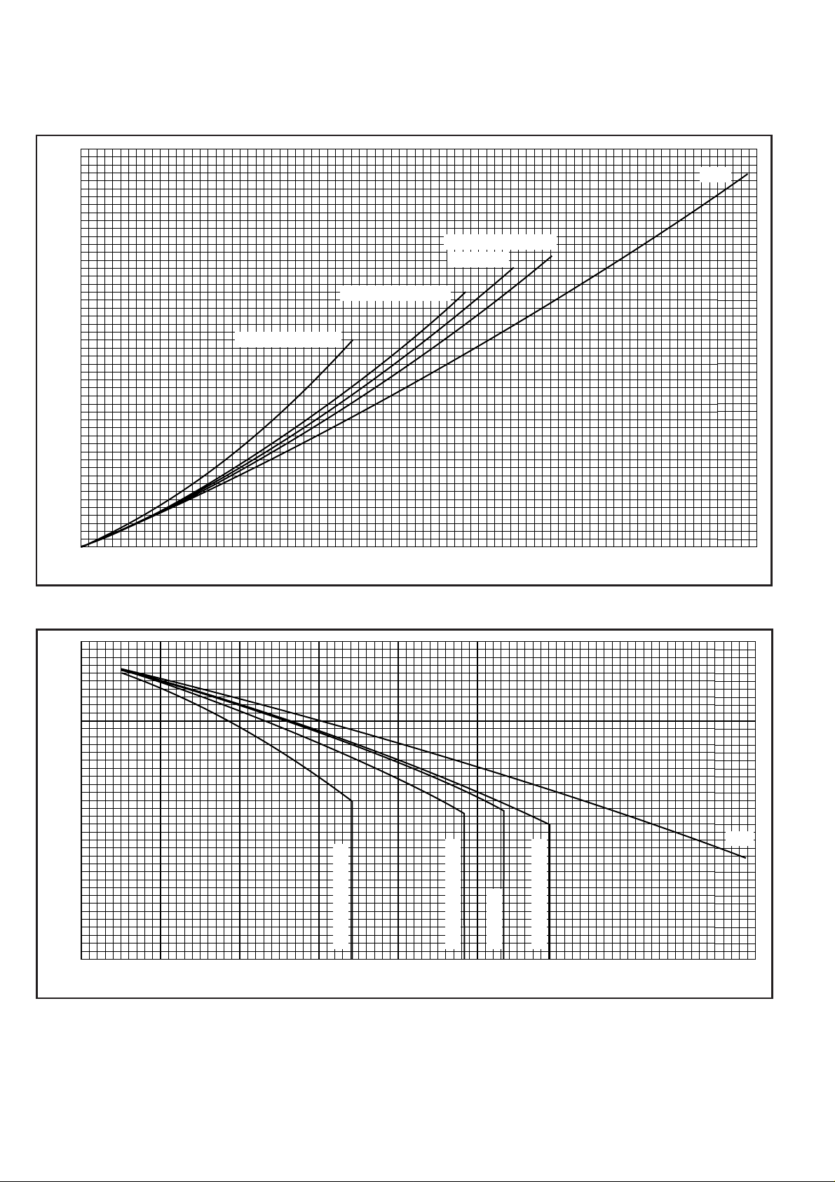
Fig. 4 On-state power loss per arm vs forward current at various conduction angles, 50/60Hz
160
140
120
300
350 400 425
100
80
60
40
20
Maximum permissible case temperature - (˚C)
0
0 50 100 150
60˚ Rectangular
120˚ Rectangular
180˚ Sine
180˚ Rectangular
250200 300
350 400 425
Forward current - (A)
Fig. 5 Maximum permissible case temperature vs forward current per arm at various conduction angles, 50/60Hz
6/9
d.c.
Page 7
1400
1200
MP03 XX 260 Series
0.020.04
0.01
R
th(hs-a)
˚C/W
R- Load
1000
0.08
L- Load
800
0.10
600
Total power - (W)
400
200
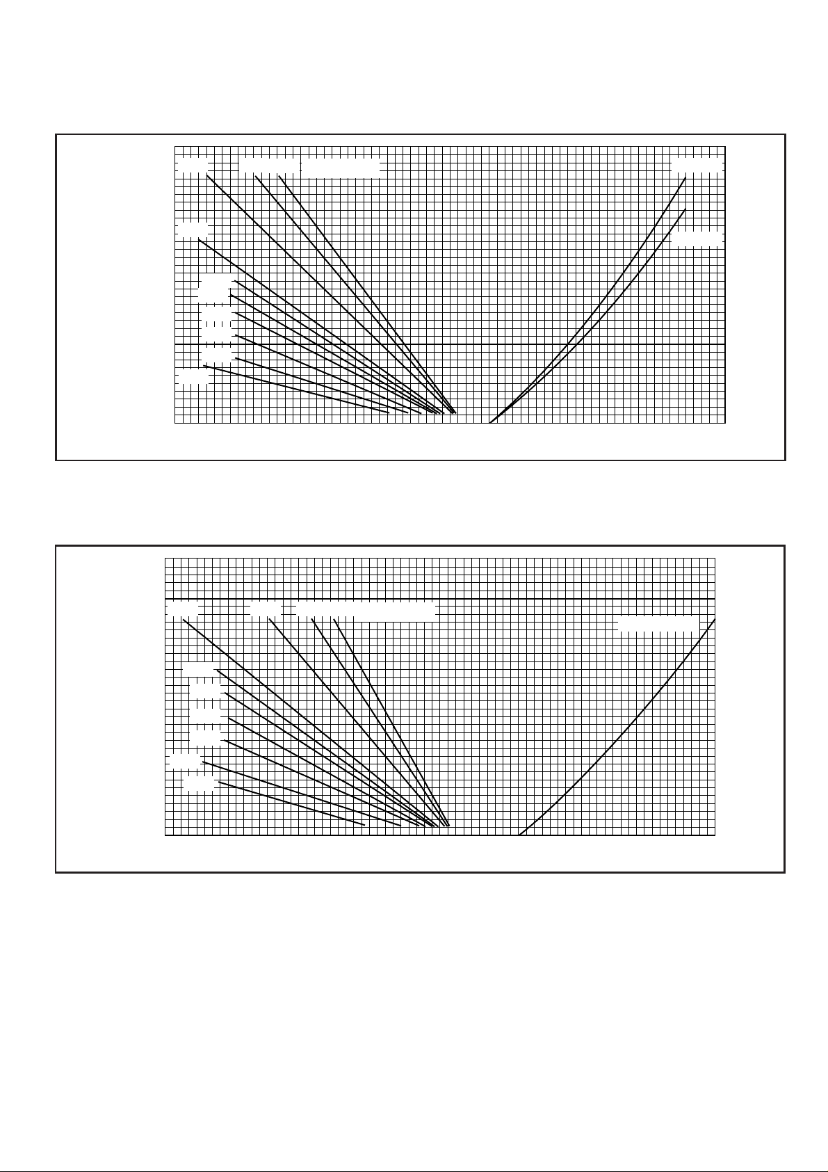
Fig. 6 50/60Hz single phase bridge dc output current vs power loss and maximum permissible ambient temperature for
(Note: R
values given above are true heatsink thermal resistances to ambient and already account for R
th(hs-a)
0.12
0.15
0.20
0.30
0.40
0
04080
20 60 100
Maximum ambient temperature - (˚C)
various values of heatsink thermal resistance.
120 140
0
D.C. output current - (A)
600400200
module contact thermal).
th(c-hs)
1400
1200
0.08 R
0.020.04
0.01
th(hs-a)
˚C/W
R & L - Load
1000
800
0.10
0.12
600
Total power - (W)
400
0.15
0.20
0.30
0.40
200
0
04080 0
Maximum ambient temperature - (˚C)
Fig. 7 50/60Hz 3- phase bridge dc output current vs power loss and maximum permissible ambient temperature for various
values of heatsink thermal resistance.
(Note: R
values given above are true heatsink thermal resistances to ambient and already account for R
th(hs-a)
120 140 160
D.C. output current - (A)
module contact thermal).
th(c-hs)
50040020020 60 100
7/9
Page 8
MP03 XX 260 Series
PACKAGE DETAILS
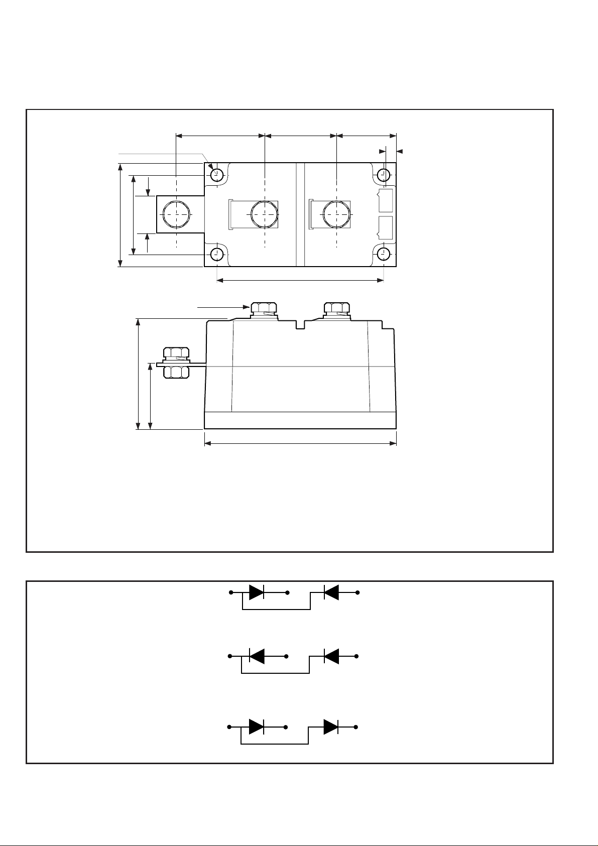
For further package information, please contact your local Customer Service Centre. All dimensions in mm, unless stated otherwise.
DO NOT SCALE.
4 holes Ø5.5
50
18
38
52
32
42.5
2x M8
1
2
35 28.5
5
80
3
CIRCUIT CONFIGURATIONS
92
Recommended fixings for mounting: M5 socket head cap screws.
Recommended mounting torque: 5Nm (44lb.ins)
Recommended torque for electrical connections: 8Nm (70lb.ins)
Maximum torque for electrical connections: 9Nm (80lb.ins)
Nominal weight: 950g
Module outline type code: MP03
1
2
3
HB
1
2
3
G
1
2
3
8/9
GN
Page 9
MP03 XX 260 Series
http://www.dynexsemi.com
e-mail: [email protected]
HEADQUARTERS OPERATIONS
DYNEX SEMICONDUCTOR LTD
Doddington Road, Lincoln.
Lincolnshire. LN6 3LF. United Kingdom.
Tel: 00-44-(0)1522-500500
Fax: 00-44-(0)1522-500550
DYNEX POWER INC.
Unit 7 - 58 Antares Drive,
Nepean, Ontario, Canada K2E 7W6.
Tel: 613.723.7035
Fax: 613.723.1518
Toll Free: 1.888.33.DYNEX (39639)
Datasheet Annotations:
Dynex Semiconductor annotate datasheets in the top right hard corner of the front page, to indicate product status. The annotations are as follows:-
Target Information: This is the most tentative form of information and represents a very preliminary specification. No actual design work on the product has been started.
Preliminary Information: The product is in design and development. The datasheet represents the product as it is understood but details may change.
Advance Information: The product design is complete and final characterisation for volume production is well in hand.
No Annotation: The product parameters are fixed and the product is available to datasheet specification.
This publication is issued to provide information only which (unless agreed by the Company in writing) may not be used, applied or reproduced for any purpose nor form part of any order or contract nor to be regarded as
a representation relating to the products or services concerned. No warranty or guarantee express or implied is made regarding the capability, performance or suitability of any product or service. The Company reserves
the right to alter without prior notice the specification, design or price of any product or service. Information concerning possible methods of use is provided as a guide only and does not constitute any guarantee that such
methods of use will be satisfactory in a specific piece of equipment. It is the user's responsibility to fully determine the performance and suitability of any equipment using such information and to ensure that any publication
or data used is up to date and has not been superseded. These products are not suitable for use in any medical products whose failure to perform may result in significant injury
or death to the user. All products and materials are sold and services provided subject to the Company's conditions of sale, which are available on request.
All brand names and product names used in this publication are trademarks, registered trademarks or trade names of their respective owners.
CUSTOMER SERVICE CENTRES
France, Benelux, Italy and Spain Tel: +33 (0)1 69 18 90 00. Fax: +33 (0)1 64 46 54 50
North America Tel: 011-800-5554-5554. Fax: 011-800-5444-5444
UK, Germany, Scandinavia & Rest Of World Tel: +44 (0)1522 500500. Fax: +44 (0)1522 500020
SALES OFFICES
France, Benelux, Italy and Spain Tel: +33 (0)1 69 18 90 00. Fax: +33 (0)1 64 46 54 50
Germany Tel: 07351 827723
North America Tel: (613) 723-7035. Fax: (613) 723-1518. Toll Free: 1.888.33.DYNEX (39639) /
Tel: (831) 440-1988. Fax: (831) 440-1989 / Tel: (949) 733-3005. Fax: (949) 733-2986.
UK, Germany, Scandinavia & Rest Of World Tel: +44 (0)1522 500500. Fax: +44 (0)1522 500020
These offices are supported by Representatives and Distributors in many countries world-wide.
© Dynex Semiconductor 2000 Publication No. DS5104-3 Issue No. 3.0 January 2000
TECHNICAL DOCUMENTATION – NOT FOR RESALE. PRINTED IN UNITED KINGDOM
9/9
 Loading...