

Page 1
19/7/02
MOC3060, MOC3061, MOC3062, MOC3063
OPTICALLY COUPLED BILATERAL
SWITCH LIGHT ACTIVATED ZERO
VOLTAGE CROSSING TRIAC
DESCRIPTION
The MOC306_ Series are optically coupled
isolators consisting of a Gallium Arsenide
infrared emitting diode coupled with a monolithic silicon detector performing the functions
of a zero crossing bilateral triac mounted in a
standard 6 pin dual-in-line package.
FEATURES
l Options :-
10mm lead spread - add G after part no.
Surface mount - add SM after part no.
Tape&reel - add SMT&R after part no.
l High Isolation Voltage, 5.3kV
l Zero Voltage Crossing
l 600V Peak Blocking Voltage
l All electrical parameters 100% tested
l Custom electrical selections available
RMS
APPLICATIONS
l CRTs
l Power Triac Driver
l Motors
l Consumer appliances
l Printers
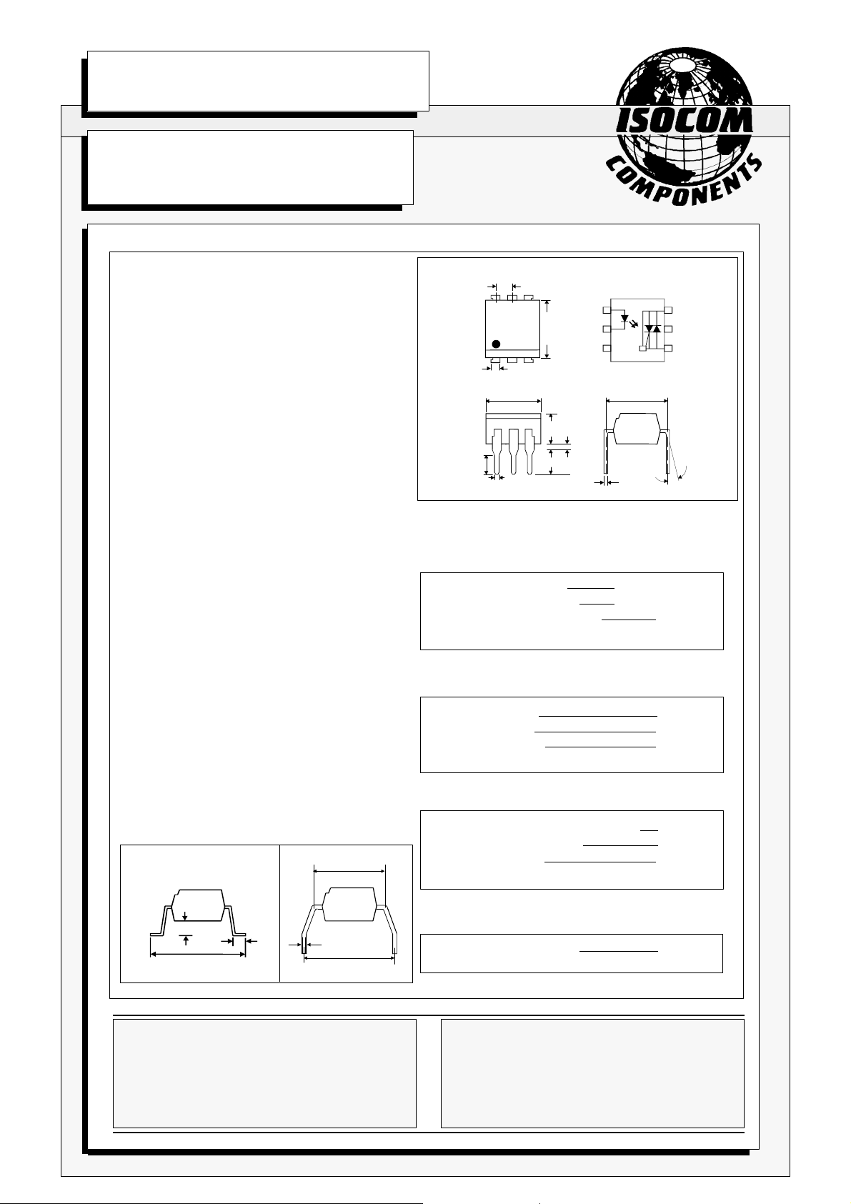
Dimensions in mm
1
2 5
3 4
7.62
0.26
6
13°
Max
1.2
3.0
7.62
6.62
2.54
0.5
7.0
6.0
4.0
3.0
0.5
3.35
ABSOLUTE MAXIMUM RATINGS
(25 °C unless otherwise noted)
Storage Temperature -550C - +1500C
Operating Temperature -400C - +1000C
Lead Soldering Temperature 2600C
(1.6mm from case for 10 seconds)
INPUT DIODE
Forward Current 50mA
Reverse Voltage 6V
Power Dissipation 120mW
(derate linearly 1.41mW/0C above 250C)
OPTION SM
SURFACE MOUNT
0.6
0.1
10.46
9.86
1.25
0.75
OPTION G
7.62
0.26
10.16
ISOCOM COMPONENTS LTD
Unit 25B, Park View Road West,
Park View Industrial Estate, Brenda Road
Hartlepool, TS25 1YD England Tel: (01429)863609
Fax : (01429) 863581 e-mail [email protected]
http://www.isocom.com
OUTPUT PHOTO TRIAC
Off-State Output Terminal Voltage 600V
Forward Current (Peak) 1A
Power Dissipation 150mW
(derate linearly 1.76mW/0C above 250C)
POWER DISSIPATION
Total Power Dissipation 250mW
(derate linearly 2.94mW/0C above 250C)
ISOCOM INC
1024 S. Greenville Ave, Suite 240,
Allen, TX 75002 USA
Tel: (214) 495-0755 Fax: (214) 495-0901
e-mail [email protected]
http://www.isocom.com
DB91051m-AAS/A6
Page 2

19/7/02
ELECTRICAL CHARACTERISTICS ( TA = 25°C Unless otherwise noted )
PARAMETER MIN TYP MAX UNITS TEST CONDITION
Input Forward Voltage (VF) 1.2 1.4 V IF = 20mA
Reverse Current (IR) 0.05 10 µA VR = 6V
Output Peak Off-state Current ( I
Peak Blocking Voltage ( V
On-state Voltage ( V
TM
) 500 nA V
DRM
) 600 V I
DRM
= 600V (note 1 )
DRM
= 500nA
DRM
) 3.0 V ITM = 100mA ( peak )
Critical rate of rise of
off-state Voltage ( dv/dt ) 600 1500 V/µs
Coupled Input Current to Trigger ( IFT )(note 2 )
MOC3060 30 mA VTM = 3V ( note 2 )
MOC3061 15 mA
MOC3062 10 mA
MOC3063 5 mA
Holding Current , either direction ( IH ) 400 µA
Input to Output Isolation Voltage V
Zero Inhibit Voltage ( VIH ) 20 V IF= Rated I
Crossing MT1-MT2 Voltage
5300 V
ISO
RMS
See note 3
FT
Charact- above which device
-eristic will not trigger
Leakage in Inhibited State ( IS ) 500 µA IF= Rated I
V
DRM
FT
= 600V off-state
Note 1. Test voltage must be applied within dv/dt rating.
Note 2. Guaranteed to trigger at an IF value less than or equal to max. I
between Rated I
Note 3. Measured with input leads shorted together and output leads shorted together.
and absolute max. IF .
FT
, recommended IF lies
FT
DB91051m-AAS/A6
Page 3

CHARACTERISTIC CURVES
Fig.1 Forward Current vs. Fig.2 On-state Current vs. Ambient
Ambient Temperature
60
Temperature
50
(mA)
40
F
30
20
Forward current I
10
0
-40
0 20 40 60 80 100
Ambient temperature Ta ( C) Ambient temperature Ta ( C)
Fig.3 Minimum Trigger Current
vs. Ambient Temperature
10
(mA)
8
FT
6
4
2
Minimum trigger current I
0
20
Ambient temperature ( C)
0.10
0.05
TM
I , on-state current (A)
120-20 -40 -20 0 804020 60 100 120
o
0
Fig.4 Forward Current vs. Forward
Voltage
VP=6V
RL=100
806040
o
100
100
(mA)
F
Forward current I
80 C
100 C
10
1
0.4
o
o
0.8 1.2 1.6
Forward voltage VF (V)
o
60 C
40 C
20 C
o
o
o
2.0
Fig.5 On-state Voltage vs. Ambient
Temperature
(V)
TM
On-state voltage V
3.0
2.6
2.2
1.8
1.4
1.0
40 8060
Ambient temperature Ta ( C) Ambient Temperature Ta ( C)
ITM =100mA
100
o
Fig.6 Holding Current vs.
Ambient Temperature
1
(mA)
H
0.1
Forward current I
0.01
20 40 60 80 10020
VP=6V
o
19/07/02 DB91051m-AAS/A6
Page 4
CHARACTERISTIC CURVES
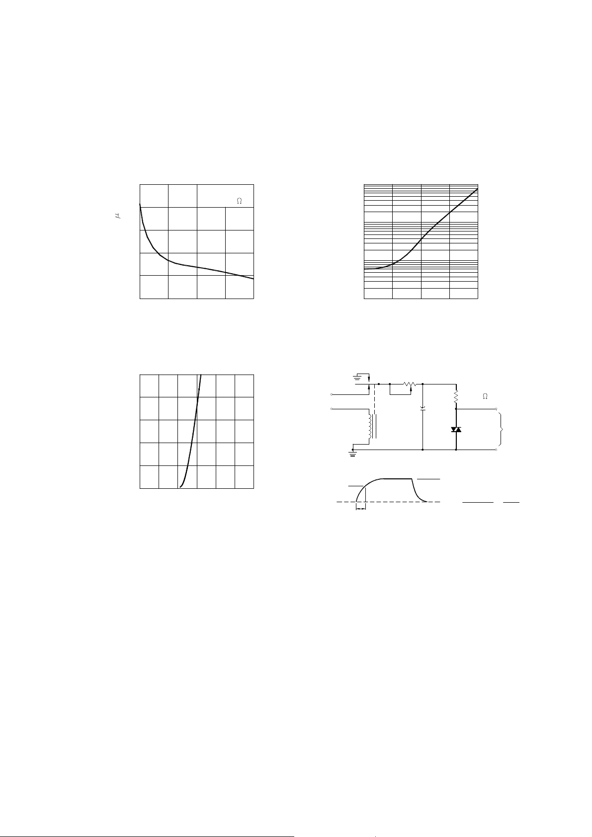
Fig.7 Turn-on Time vs. Forward
Current
10
8
s)
6
4
Turn-on time Ton (
2
0
10
Forward current I F (mA)
20 30
VP=9V
RL=100
Fig.9 On-state Current vs.
On-state Voltage
100
80
(mA)
TM
60
40
Fig.8 Repetitive Peak Off-state Current
vs. Temperature
1000
100
10
Idrm (nA)
Repetitive Peak Off-state Current
40 50 20
1
Static dv/dt Test Circuit
+400
Vdc
PULSE
INPUT
Ambient temperature Ta ( C)
RTEST
CTEST
MERCURY
WETTED
RELAY
O
D.U.T.
10040 60 80
R=10k
X100
SCOPE
PROBE
20
On-state current I
0
0.5 2.0 2.51.0
On-state voltage VTM (V)
APPLIED VOLTAGE
3.01.50
WAVEFORM
0 VOLTS
252 V
τ
RC
Vmax = 400V
0.63 Vmax
dv/dt=
τRC
378
=
τRC
19/07/02 DB91051m-AAS/A6
 Loading...