

Page 1
MOC211M, MOC212M, MOC213M — Small Ouline Optocouplers Transistor Output
April 2009
MOC211M, MOC212M, MOC213M
Small Ouline Optocouplers Transistor Output
Features
UL recognized (File #E90700, Volume 2)
■
■
VDE recognized (File #136616) (add option ‘V’ for
VDE approval, e.g., MOC211VM)
Convenient plastic SOIC-8 surface mountable
■
package style
■
Standard SOIC-8 footprint, with 0.050" lead spacing
Compatible with dual wave, vapor phase and
■
IR reflow soldering
High input-output isolation of 2500 V
■
AC(rms)
guaranteed
■
Minimum BV
of 30V guaranteed
CEO
Applications
■
General purpose switching circuits
Interfacing and coupling systems of different
■
potentials and impedances
Regulation feedback circuits
■
■
Monitor and detection circuits
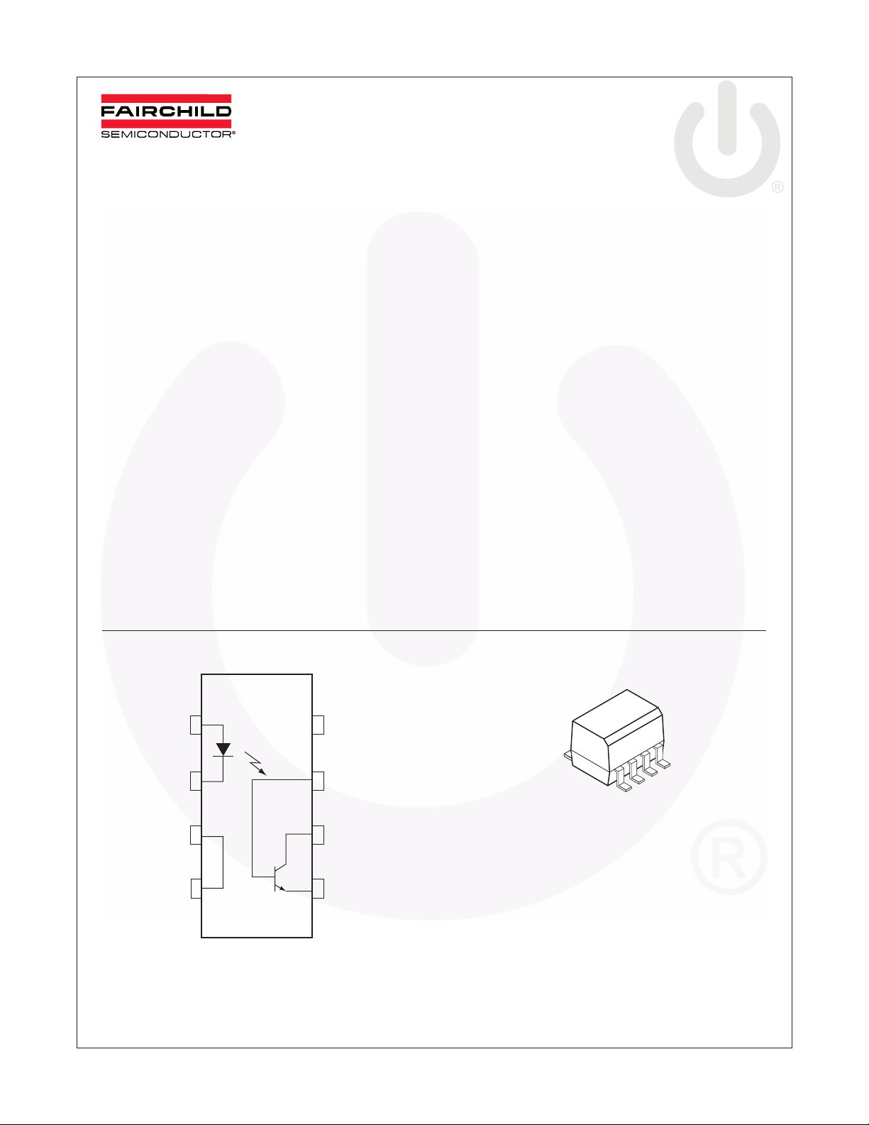
Schematic
Description
These devices consist of a gallium arsenide infrared
emitting diode optically coupled to a monolithic silicon
phototransistor detector, in a surface mountable, small
outline, plastic package. They are ideally suited for high
density applications, and eliminate the need for throughthe-board mounting.
1
N/C
2
3
4
CATHODE
©2005 Fairchild Semiconductor Corporation www.fairchildsemi.com
MOC211M, MOC212M, MOC213M Rev. 1.0.1
N/CANODE
8
7
BASE
COLLECTORN/C
6
EMITTER
5
Page 2
MOC211M, MOC212M, MOC213M — Small Ouline Optocouplers Transistor Output
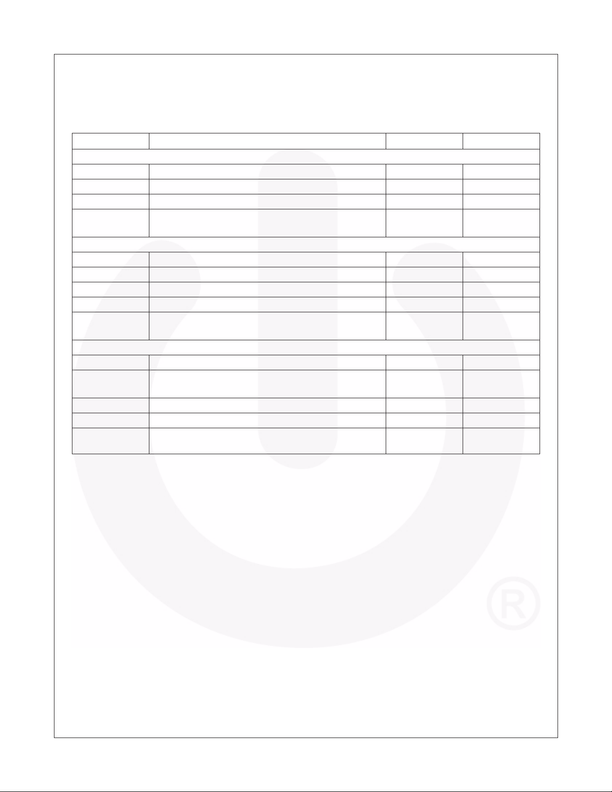
Absolute Maximum Ratings
(T
= 25°C Unless otherwise specified)
A
Stresses exceeding the absolute maximum ratings may damage the device. The device may not function or be
operable above the recommended operating conditions and stressing the parts to these levels is not recommended.
In addition, extended exposure to stresses above the recommended operating conditions may affect device reliability.
The absolute maximum ratings are stress ratings only.
Symbol Rating Value Unit
EMITTER
I
F
I
(pk) Forward Current – Peak (PW = 100µs, 120pps) 1.0 A
F
V
R
P
D
DETECTOR
V
CEO
V
ECO
V
CBO
I
C
P
D
TOTAL DEVICE
V
ISO
P
D
T
A
T
stg
T
L
Forward Current – Continuous 60 mA
Reverse Voltage 6.0 V
LED Power Dissipation @ T
Derate above 25°C
= 25°C
A
90
0.8
mW
mW/°C
Collector-Emitter Voltage 30 V
Emitter-Collector Voltage 7.0 V
Collector-Base Voltage 70 V
Collector Current-Continuous 150 mA
Detector Power Dissipation @ T
Derate above 25°C
Input-Output Isolation Voltage (f = 60Hz, t = 1 min.)
Total Device Power Dissipation @ T
Derate above 25°C
= 25°C
A
A
= 25°C
(1)(2)(3)
150
1.76
mW
mW/°C
2500 Vac(rms)
250
2.94
mW
mW/°C
Ambient Operating Temperature Range -40 to +100 °C
Storage Temperature Range -40 to +150 °C
Lead Soldering Temperature
260 °C
(1/16 " from case, 10 sec. duration)
Notes:
1. Isolation Surge Voltage, V
, is an internal device dielectric breakdown rating.
ISO
2. For this test, Pins 1 and 2 are common and Pins 5, 6 and 7 are common.
3. V
rating of 2500 V
ISO
©2005 Fairchild Semiconductor Corporation www.fairchildsemi.com
MOC211M, MOC212M, MOC213M Rev. 1.0.1 2
for t = 1 min. is equivalent to a rating of 3,000 V
AC(rms)
AC(rms)
for t = 1 sec.
Page 3

Ω
MOC211M, MOC212M, MOC213M — Small Ouline Optocouplers Transistor Output
Electrical Characteristics
(T
= 25°C unless otherwise specified)
A
Symbol Parameter Test Conditions Min. Typ.* Max. Unit
EMITTER
V
Input Forward Voltage I
F
Reverse Leakage Current V
I
R
Input Capacitance 18 pF
C
IN
DETECTOR
I
CEO1
I
CEO2
BV
Collector-Emitter Dark Current V
Collector-Emitter Breakdown
CEO
Voltage
BV
Emitter-Collector Breakdown
ECO
Voltage
C
Collector-Emitter Capacitance f = 1.0MHz, V
CE
COUPLED
CTR Collector-Output Current
MOC211M
MOC212M
MOC213M
V
R
V
CE (sat)
C
Isolation Surge Voltage
ISO
Isolation Resistance
ISO
Collector-Emitter Saturation Voltage I
Isolation Capacitance
ISO
Tu r n-On Time I
t
on
Tu r n-Off Time I
t
off
Rise Time I
t
r
Fall Time I
t
f
(2)
(2)
(4)
(1)(2)(3)
= 10mA 1.15 1.5 V
F
= 6.0V 0.001 100 µA
R
= 10V, T
CE
= 10V, T
V
CE
I
= 100µA 30 100 V
C
I
= 100µA 7.0 10 V
E
= 10mA, V
I
F
= 25°C
A
= 100°C
A
= 0 7.0 pF
CE
= 10V
CE
1.0
1.0
50 nA
µA
20
50
100
f = 60 Hz AC Peak, t = 1 min. 2500 Vac(rms)
V = 500V 10
= 2.0mA, I
C
= 10mA 0.4 V
F
11
V = 0V, f = 1MHz 0.2 pF
= 2.0mA, V
C
= 10V, R
CC
= 100 Ω
L
7.5 µs
(Fig. 10)
= 2.0mA, V
C
= 10V, R
CC
= 100 Ω
L
5.7 µs
(Fig. 10)
= 2.0mA, V
C
= 10V, R
CC
= 100 Ω
L
3.2 µs
(Fig. 10)
= 2.0mA, V
C
= 10V, R
CC
= 100 Ω
L
4.7 µs
(Fig. 10)
%
*Typical values at T
= 25°C
A
Notes:
1. Isolation Surge Voltage, V
, is an internal device dielectric breakdown rating.
ISO
2. For this test, Pins 1 and 2 are common and Pins 5, 6 and 7 are common.
rating of 2500 V
3. V
ISO
4. Current Transfer Ratio (CTR) = I
©2005 Fairchild Semiconductor Corporation www.fairchildsemi.com
MOC211M, MOC212M, MOC213M Rev. 1.0.1 3
for t = 1 min. is equivalent to a rating of 3,000 V
AC(rms)
/I
x 100%.
C
F
AC(rms)
for t = 1 sec.
Page 4
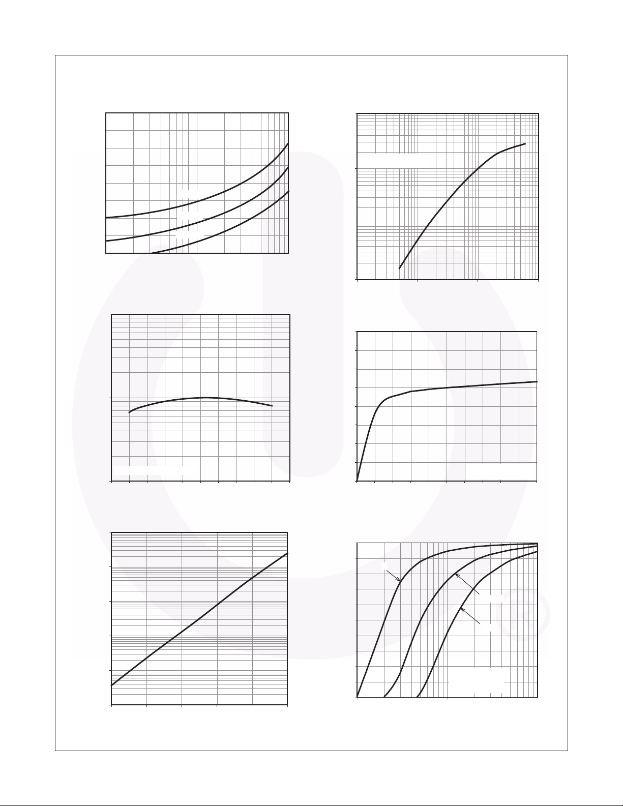
Typical Performance Curves
MOC211M, MOC212M, MOC213M — Small Ouline Optocouplers Transistor Output
Fig. 1 LED Forward Voltage vs. Forward Current
1.8
1.7
1.6
1.5
1.4
1.3
1.2
– FORWARD VOLTAGE (V)
F
V
1.1
1.0
110100
TA = –55°C
TA = 25°C
TA = 100°C
IF – LED FORWARD CURRENT (mA)
Fig. 3 Output Current vs. Ambient Temperature
10
1
10
VCE = 5V
NOR MALIZE D TO I
1
0.1
– OUTPUT COLLECT OR CURRENT (NORMALIZED)
C
I
0.01
0.1 1 1 0 100
= 10 mA
F
IF – LED INPUT CURRENT (mA)
Fig. 4 Output Current vs. Collector-Emitter Voltage
1.6
1.4
1.2
1.0
0.8
Fig. 2 Output Curent vs. Input Current
– OUTPUT COLLECT OR CUR RENT (N ORM ALIZE D)
C
I
NORMALIZED TO TA = 25°C
0.1
-80 -60 -40 -20 0 2 0 40 60 80 100 120
TA – AMBIENT TEMPERATURE (°C)
Fig. 5 Dark Current vs. Ambient Temperature
1000 0
V
= 10V
CE
1000
100
10
1
– COLLECTOR -E MIT TER DA RK CU RRE NT (nA )
CEO
I
0.1
020406080100
TA – AMBIENT TEMPERATURE (°C)
0.6
0.4
0.2
– OUTPUT COLLECTOR CURRENT (NORMALIZED)
C
0.0
I
012345678910
IF = 10 mA
NORM ALIZE D TO V
VCE – COLLECTOR-EMITTER VOLTAGE (V)
Fig. 6 CTR vs. RBE (Unsaturated)
1.0
0.9
IFmA
= 20
0.8
0.7
0.6
0.5
0.4
NORMALIZED CTR
0.3
0.2
0.1
0.0
10 100 1000
V
Normalized to:
CTR at R
RBE – BASE RESISTANCE (kΩ)
CE
= 5V, T
=
I
F
I
= 5mA
F
A
= Open
BE
10mA
=
25°C
= 5V
CE
©2005 Fairchild Semiconductor Corporation www.fairchildsemi.com
MOC211M, MOC212M, MOC213M Rev. 1.0.1 4
Page 5
MOC211M, MOC212M, MOC213M — Small Ouline Optocouplers Transistor Output
Typical Performance Curves
1.0
0.9
0.8
0.7
0.6
0.5
0.4
NORMALIZED CTR
0.3
0.2
0.1
0.0
10 100 1000
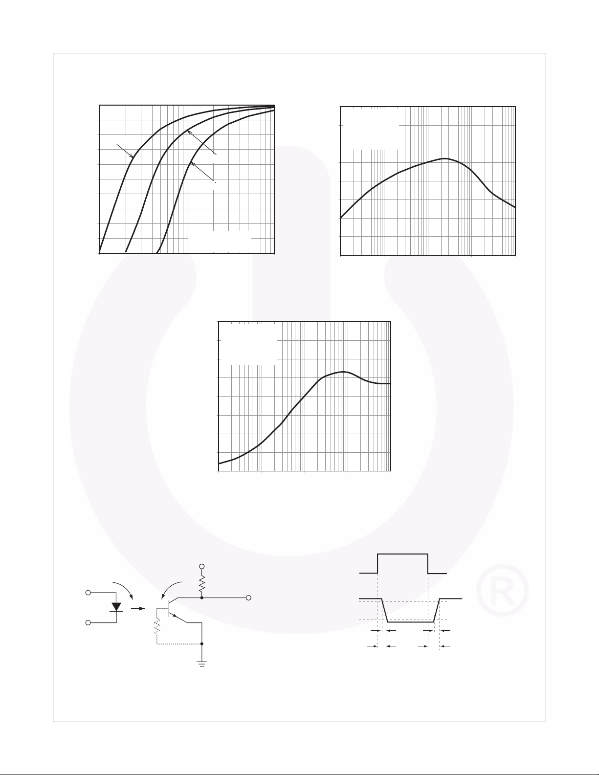
Fig. 7 CTR vs. RBE (Saturated)
= 20mA
I
F
RBE –
BASE RESISTANCE (kΩ)
I
= 10mA
F
I
= 5mA
F
V
= 0.3V, TA = 25°C
CE
Normalized to:
CTR at R
BE
1.6
1.4
1.2
offf
1.0
= Open
(Continued)
Fig. 9 Normalized t
V
= 10V
CC
I
= 2mA
C
= 100
Ω
R
L
NORMALIZED TO :
AT RBE = OPEN
t
offf
Fig. 8 Normalized ton vs. R
4.0
V
= 10V
CC
= 2mA
I
C
3.5
= 100Ω
R
L
NORMALIZED TO :
3.0
t
AT RBE = OPEN
on
on
2.5
2.0
ALIZED t
1.5
NORM
1.0
0.5
0.0
0.01 0.1 1 10 100
R
–
BASE RESISTANCE (MΩ )
BE
vs. R
off
BE
BE
INPUT
TEST CIRCUIT
I
F
R
BE
0.8
0.6
NORMALIZED t
0.4
0.2
0.0
0.01 0.1 1 10 100
(M
Ω
RBE – BASE RESISTANCE
)
WAVEFORMS
= 10V
V
CC
INPUT PULSE
I
C
R
L
OUTPUT
I
Adjust
F to produce IC = 2mA
10%
90%
OUTPUT PULSE
t
r
t
on
t
f
t
off
Figure 10. Switching Time Test Circuit and Waveforms
©2005 Fairchild Semiconductor Corporation www.fairchildsemi.com
MOC211M, MOC212M, MOC213M Rev. 1.0.1 5
Page 6
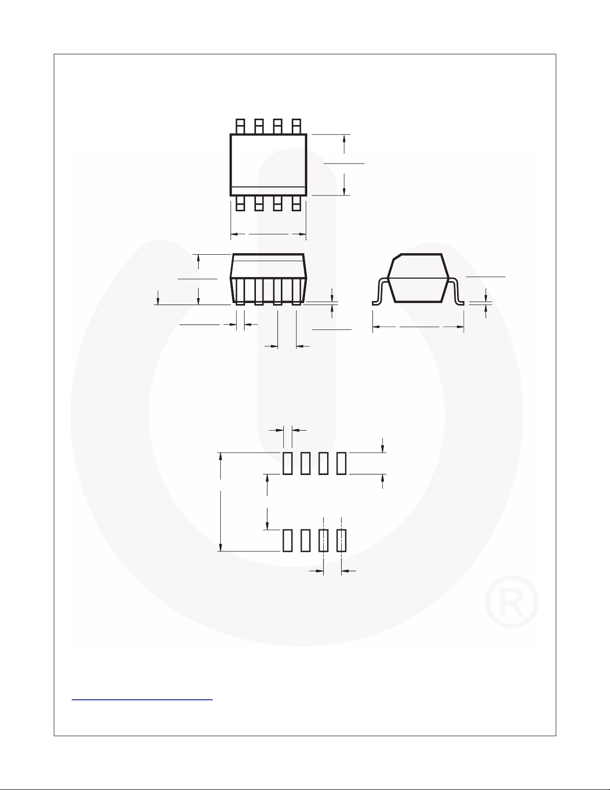
Package Dimensions
8-pin SOIC Surface Mount
8
1
0.202 (5.13)
0.182 (4.63)
0.164 (4.16)
0.144 (3.66)
MOC211M, MOC212M, MOC213M — Small Ouline Optocouplers Transistor Output
0.143 (3.63)
0.123 (3.13)
SEATING PLANE
0.021 (0.53)
0.011 (0.28)
Lead Coplanarity: 0.004 (0.10) MAX
Recommended Pad Layout
0.050 (1.27) Typ.
0.275 (6.99)
0.155 (3.94)
0.008 (0.20)
0.003 (0.08)
0.024 (0.61)
0.010 (0.25)
0.006 (0.16)
0.244 (6.19)
0.224 (5.69)
0.060 (1.52)
0.050 (1.27)
Dimensions in inches (mm).
Package drawings are provided as a service to customers considering Fairchild components. Drawings may change in any manner
without notice. Please note the revision and/or date on the drawing and contact a Fairchild Semiconductor representative to verify or
obtain the most recent revision. Package specifications do not expand the terms of Fairchild’s worldwide terms and conditions,
specifically the warranty therein, which covers Fairchild products.
Always visit Fairchild Semiconductor’s online packaging area for the most recent package drawings:
http://www
©2005 Fairchild Semiconductor Corporation www.fairchildsemi.com
MOC211M, MOC212M, MOC213M Rev. 1.0.1 6
.fairchildsemi.com/packaging/
Page 7
Ordering Information
Option Order Entry Identifier Description
VVVDE 0884
R2 R2 Tape and reel (2500 units per reel)
R2V R2V VDE 0884, Tape and reel (2500 units per reel)
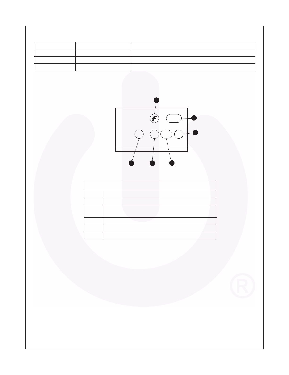
Marking Information
1
MOC211M, MOC212M, MOC213M — Small Ouline Optocouplers Transistor Output
211
SYYXV
43
5
2
6
Definitions
1Fairchild logo
2Device number
3 VDE mark (Note: Only appears on parts ordered with VDE
option – See order entry table)
4 One digit year code, e.g., ‘8’
5Two digit work week ranging from ‘01’ to ‘53’
6 Assembly package code
©2005 Fairchild Semiconductor Corporation www.fairchildsemi.com
MOC211M, MOC212M, MOC213M Rev. 1.0.1 7
Page 8
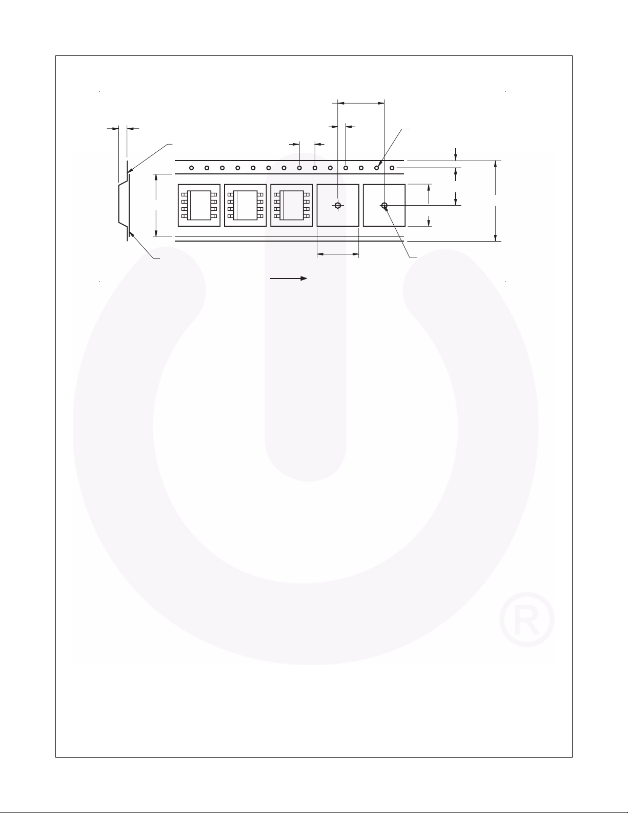
Carrier Tape Specifications
8.0 ± 0.10
MOC211M, MOC212M, MOC213M — Small Ouline Optocouplers Transistor Output
3.50 ± 0.20
0.30 MAX
8.3 ± 0.10
0.1 MAX
Dimensions in mm
4.0 ± 0.10
User Direction of Feed
2.0 ± 0.05
6.40 ± 0.20
Ø1.5 MIN
1.75 ± 0.10
5.5 ± 0.05
12.0 ± 0.3
5.20 ± 0.20
Ø1.5 ± 0.1
©2005 Fairchild Semiconductor Corporation www.fairchildsemi.com
MOC211M, MOC212M, MOC213M Rev. 1.0.1 8
Page 9
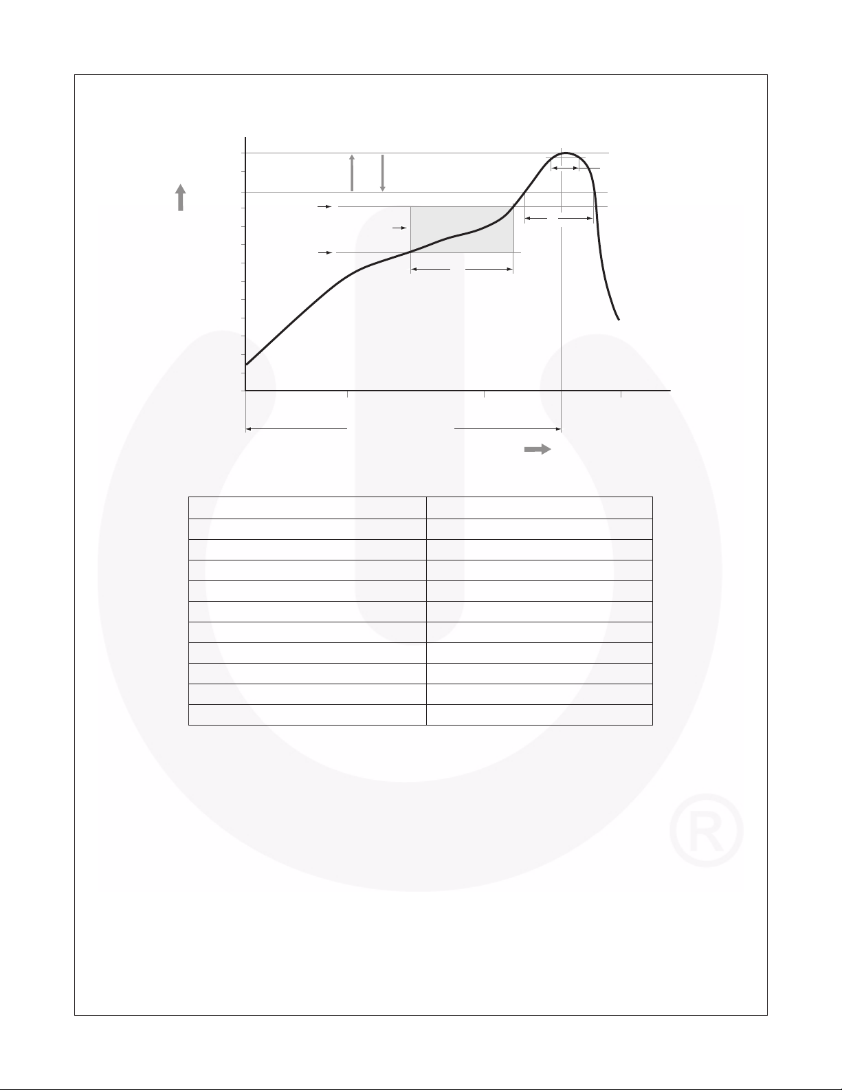
Reflow Profile
MOC211M, MOC212M, MOC213M — Small Ouline Optocouplers Transistor Output
Max. Ramp-up Rate = 3°C/S
Max. Ramp-down Rate = 6°C/S
Ts ma x
Preheat Area
Ts mi n
t
L
t
s
260
240
220
200
180
160
140
120
T
P
T
L
100
80
60
Temperature (°C)
40
20
0
120
240 360
Time 25°C to Peak
Time (seconds)
Profile Freature Pb-Free Assembly Profile
Temperature Min. (Tsmin) 150°C
Temperature Max. (Tsmax) 200°C
Time (t
Ramp-up Rate (t
Liquidous Temperature (T
Time (t
Peak Body Package Temperature 260°C +0°C / –5°C
Time (t
Ramp-down Rate (T
Time 25°C to Peak Temperature 8 minutes max.
) from (Tsmin to Tsmax) 60–120 seconds
S
to t
) 3°C/second max.
L
P
) 217°C
L
) Maintained Above (TL) 60–150 seconds
L
) within 5°C of 260°C 30 seconds
P
to TL) 6°C/second max.
P
t
P
©2005 Fairchild Semiconductor Corporation www.fairchildsemi.com
MOC211M, MOC212M, MOC213M Rev. 1.0.1 9
Page 10
TRADEMARKS
The following includes registered and unregistered trademarks and service marks, owned by Fairchild Semiconductor and/or its global subsidiaries,andis not
intended to be an exhaustive list of all such trademarks.
Auto-SPM™
Build it Now™
CorePLUS™
CorePOWER™
CROSSVOLT™
CTL™
Current Transfer Logic™
EcoSPARK
EfficentMax™
EZSWITCH™*
®
™*
®
®
Fairchild
Fairchild Semiconductor
FACT Quiet Series™
®
FACT
®
FAST
®
F-PFS™
®
FRFET
Global Power Resource
Green FPS™
Green FPS™ e-Series™
Gmax™
GTO™
IntelliMAX™
ISOPLANAR™
MegaBuck™
MICROCOUPLER™
MicroFET™
MicroPak™
MillerDrive™
MotionMax™
Motion-SPM™
OPTOLOGIC
OPTOPLANAR
®
®
FastvCore™
FETBench™
FlashWriter
FPS™
®
*
PDP SPM™
Power-SPM™
PowerTrench
SM
PowerXS™
Programmable Active Droop™
QFET
QS™
Quiet Series™
RapidConfigure™
Saving our world, 1mW/W/kW at a time™
SmartMax™
SMART START™
SPM
STEALTH™
SuperFET™
SuperSOT™-3
®
SuperSOT™-6
SuperSOT™-8
SupreMOS™
SyncFET™
Sync-Lock™
®
®
ThePower Franchise
TinyBoost™
TinyBuck™
®
TinyLogic
®
TINYOPTO™
™
TinyPower™
TinyPWM™
TinyWire™
TriFault Detect™
®
TRUECURRENT™*
µSerDes™
®
UHC
Ultra FRFET™
UniFET™
VCX™
VisualMax™
®
*
XS™
*Trademarks of System General Corporation, used under license by Fairchild Semiconductor.
DISCLAIMER
FAIRCHILD SEMICONDUCTOR RESERVES THE RIGHT TO MAKE CHANGES WITHOUT FURTHER NOTICE TO ANYPRODUCTS HEREIN TO IMPROVE
RELIABILITY, FUNCTION, OR DESIGN. FAIRCHILD DOES NOT ASSUME ANY LIABILITY ARISING OUT OF THE APPLICATION OR USE OF ANY PRODUCT OR
CIRCUIT DESCRIBED HEREIN; NEITHER DOES IT CONVEY ANY LICENSE UNDER ITS PATENT RIGHTS, NOR THE RIGHTS OF OTHERS. THESE
SPECIFICATIONS DO NOT EXPAND THE TERMS OF FAIRCHILD’S WORLDWIDE TERMS AND CONDITIONS, SPECIFICALLY THE WARRANTY THEREIN,
WHICH COVERS THESE PRODUCTS.
MOC211M, MOC212M, MOC213M — Small Ouline Optocouplers Transistor Output
LIFE SUPPORT POLICY
FAIRCHILD’S PRODUCTS ARE NOT AUTHORIZED FOR USE AS CRITICAL COMPONENTS IN LIFE SUPPORT DEVICES OR SYSTEMS WITHOUT THE
EXPRESS WRITTEN APPROVAL OF FAIRCHILD SEMICONDUCTOR CORPORATION.
As used herein:
1. Life support devices or systems are devices or systems which, (a) are
intended for surgical implant into the body or (b) support or sustain life,
and (c) whose failure to perform when properly used in accordance
with instructions for use provided in the labeling, can be reasonably
expected to result in a significant injury of the user.
2. A critical component in any component of a life support, device, or
system whose failure to perform can be reasonably expected to
cause the failure of the life support device or system, or to affect its
safety or effectiveness.
ANTI-COUNTERFEITING POLICY
Fairchild Semiconductor Corporation's Anti-Counterfeiting Policy. Fairchild's Anti-Counterfeiting Policy is also stated on our external website, www.fairchildsemi.com,
under Sales Support.
Counterfeiting of semiconductor parts is a growing problem in the industry. All manufacturers of semiconductor products are experiencing counterfeiting of their parts.
Customers who inadvertently purchase counterfeit parts experience many problems such as loss of brand reputation, substandard performance, failedapplications,
and increased cost of production and manufacturing delays. Fairchild is taking strong measures to protect ourselves and our customers from the proliferation of
counterfeit parts. Fairchild strongly encourages customers to purchase Fairchild parts either directly from Fairchild or from Authorized Fairchild Distributors who are
listed by country on our web page cited above. Products customers buy either from Fairchild directly or from Authorized Fairchild Distributors are genuine parts, have
full traceability, meet Fairchild's quality standards for handling and storage and provide access to Fairchild's full range of up-to-date technicalandproduct information.
Fairchild and our Authorized Distributors will stand behind all warranties and will appropriately address any warranty issues that may arise. Fairchild will not provide
any warranty coverage or other assistance for parts bought from Unauthorized Sources. Fairchild is committed to combat this global problem and encourage our
customers to do their part in stopping this practice by buying direct or from authorized distributors.
PRODUCT STATUS DEFINITIONS
Definition of Terms
Datasheet Identification Product Status Definition
Advance Information Formative / In Design
Preliminary
First Production
No Identification Needed Full Production
Obsolete Not In Production
Datasheet contains the design specifications for product development. Specifications may change in
any manner without notice.
Datasheet contains preliminary data; supplementary data will be published at a later date. Fairchild
Semiconductor reserves the right to make changes at any time without notice to improve design.
Datasheet contains final specifications. Fairchild Semiconductor reserves the right to make changes
at any time without notice to improve the design.
Datasheet contains specifications on a product that is discontinued by Fairchild Semiconductor.
The datasheet is for reference information only.
Rev. I40
©2005 Fairchild Semiconductor Corporation www.fairchildsemi.com
MOC211M, MOC212M, MOC213M Rev. 1.0.1 10
 Loading...