

Page 1
For Information Equipment
MN89303A
SVGA Display Controller
Overview
The MN89303A is an LCD/CRT display controller with
IBM™ VGA-compatible registers. It features all the necessary interfaces for a compact display system: ISA bus interface, local bus interface, DRAM interface, and LCD panel
interface. The built-in graphics acceleration functions include
support for hardware cursor.
Note: IBM™ and VGA are registered tr ademarks of International
Business Machines Corporation.
Features
Monochrome STN LCD panel support
Maximum display size: 800 × 600
Support for single and dual panels
16-monochrome gradation
Color STN LCD panel support
Maximum display size: 800 × 600
Support for single and dual panels
16-gradation for each color (RGB)
Color TFT LCD panel support
Maximum display size: 800 × 600
4-bit output for each color (RGB)
Maximum number of colors in concurrent display
640 × 480: 256/4096 palette (TFT, STN)
800 × 600: 256/4096 palette (TFT, STN)
Built-in graphics acceleration functions
• Hardware cursor (16 × 16 or 32 × 32)
Built-in automatic display centering
Built-in gradation control table (rewritable) for
optimizing gradation to match panel
DRAM interface with 16-bit bus
• Choice of DRAM access timing to match
system performance (EDO/normal)
• Support for 2CAS/2WE mode
• Refresh control
Host interfaces
• ISA bus (16-bit)
• i386/i486 local bus (16-bit)
Note: i386 and i486 are trademarks of Intel Corporation.
Applications
Point-of-sale terminals, Factory automation terminals,
word processors, and other terminals
325
Page 2
MN89303A For Information Equipment
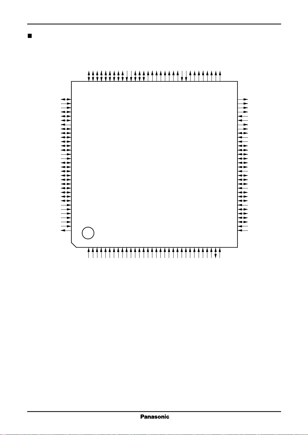
Pin Assignment
DDVSS
LOGICON
LCDON
BACKON
LD0
LD1
LD2
LD3
LD4
LD5
LD6
LD7
VDDVSSUD0
UD1
UD2
UD3
UD4
UD5
UD6
MA1
MA2
MA3
MA4
MA5
MA6
MA7
MA8
MA9
V
UD7
MAO
V
V
RAS
UCAS
LCAS
WE
MD15
MD14
MD13
MD12
MD11
MD10
V
V
MD9
MD8
MD7
MD6
MD5
MD4
MD3
MD2
MD1
MD0
V
V
RESET
MINTEST
TEST
V
XOUT
96959493929190898887868584838281807978777675747372717069686766
97
98
SS
DD
DD
DD
99
100
101
102
103
104
105
106
107
108
109
110
SS
111
112
113
114
115
116
117
118
119
120
121
122
SS
123
124
125
126
127
SS
128
12345678910111213141516171819202122232425262728293031
65
64
63
62
61
60
59
58
57
56
55
54
53
52
51
50
49
48
47
46
45
44
43
42
41
40
39
38
37
36
35
34
33
FP
LP
DISP
DCLK
V
DD
V
SS
IOCS16
MEMCS16
IOCHRDY
V
DD
V
SS
SD0
SD1
SD2
SD3
SD4
SD5
V
SS
SD6
SD7
SD8
V
DD
SD9
SD10
SD11
V
SS
SD12
SD13
SD14
SD15
V
DD
V
SS
32
SS
V
XIN
Note: Never leave V
AEN
IORD
SBHE
IOWR
SMEMR
SMEMW
and VSS pins open.
DD
A21
A20
SA19
SA18
SA17
SA16
SA15
SA14
SA13
SA12
(TOP VIEW)
QFH128-P-1818
SA11
SA10
SA9
SA8
SA7
SA6
SA5
SA4
SA3
SA2
SA1
SA0
BIOSEN
REFRESH
Page 3
For Information Equipment MN89303A
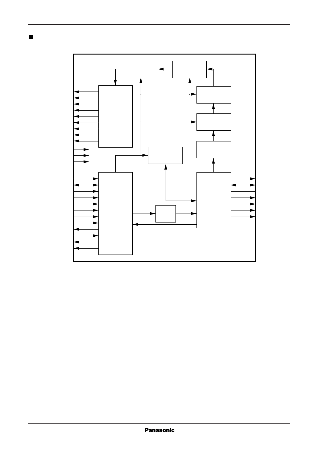
Block Diagram
UD[7:0]
LD[7:0]
BACKON
LCDON
LOGICON
DISP
DCLK
XIN
RESET
TEST/MINTEST
Address[21:0]
SD[15:0]
AEN
SBHE
IOWR
IORD
SMEMW
SMEMR
IOCHRDY
REFRESH
MEMCS16
IOCS16
Gray scale
engine
RAM table
Hardware
cursor
Attribute
control
Video FIFO
LP
FO
83
84
85
63
64
62
61
1
124
126/125
LCD panel
controller
LCD/CRT
controller
Memory
3 100
4
5
6
7
8
56
32
57
58
Host
interface
Memory
write
buffer
interface
Access
attributer
Graphics
controller
101
102
103
31
MA[9:0]
MD[15:0]
RAS
UCAS
LCAS
WE
BIOSEN
Page 4
MN89303A For Information Equipment
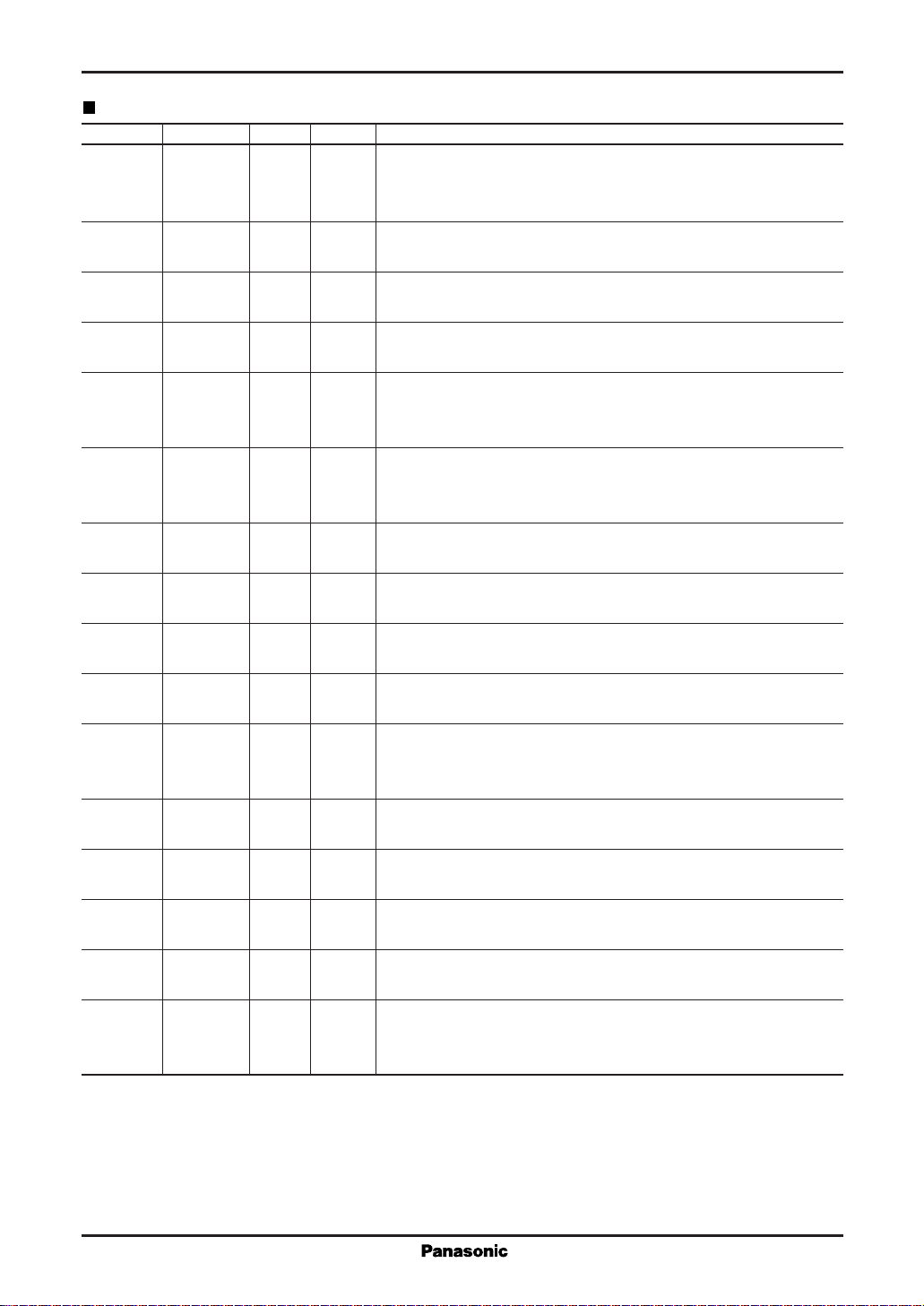
Pin Descriptions
Pin No. Symbol I/O Level Function Description
3 AEN I TTL Address Enable
"H" level input from this pin indicates that a DMA transfer is in
progress, so the chip does not respond to I/O access.
4 SBHE I TTL Byte High Enable
This input indicates the state of the 16-bit bus.
5 IOWR I TTL I/O Write
This input indicates an I/O write request.
6 IORD I TTL I/O Read
This input indicates an I/O read request.
7 SMEMW I TTL Memory Write
This input indicates a memory write request dedicated for an address
space in the first megabyte (000000 to 0FFFFFH).
8 SMEMR I TTL Memory Read
This input indicates a memory read request dedicated for an address
space in the first megabyte (000000 to 0FFFFFH).
9 to 10 A[21:20] I TTL Address[21:20]
These inputs give the address 21:20.
11 to 30 SA[19:0] I TTL Address[19:0]
These inputs give the address 19:0.
35 to 53 SD[15:0] I/O TTL Data[15:0]
These pins represent the host data bus.
56 IOCHRDY I/O TTL I/O Channel Ready
This pin is "L" level when I/O or memory access is given wait state.
57 MEMCS16 O TTL Memory Chip Select 16
This output indicates to the system that 16-bit memory access is
available.
58 IOCS16 O TTL I/O Chip Select 16
This output indicates to the system that 16-bit I/O access is available.
32 REFRESH I TTL Refresh
"L" level input indicates that the system is refreshing its DRAM.
88 to 97 MA[9:0] O CMOS Memory Address
These outputs give the address of the display memory.
100 RAS O CMOS Row Address Strobe (RAS)
This output is the strobe signal for the row address latch.
101 UCAS O CMOS Upper Column Address Strobe (UCAS)
This output is the strobe signal for the upper column address latch.
In the 2WE mode, however, it functions as the CAS signal.
Page 5
For Information Equipment MN89303A
Pin Descriptions (continued)
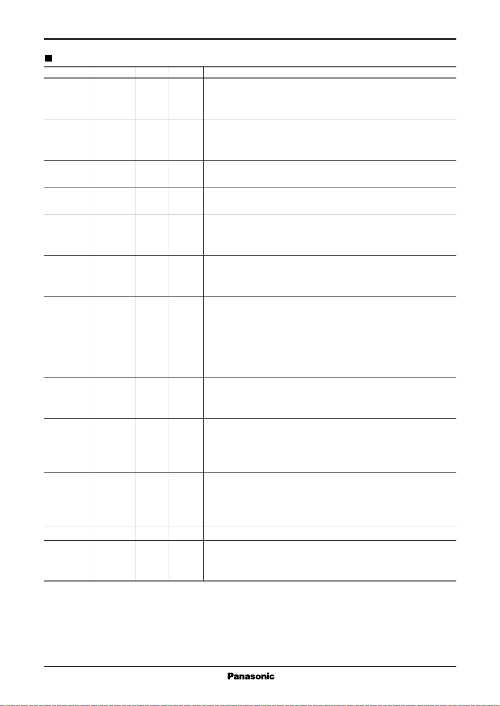
Pin No. Symbol I/O Level Function Description
102 LCAS O CMOS Lower Column Address Strobe (LCAS)
This output is the strobe signal for the lower column address latch.
In the 2WE mode, however, it functions as the LWE signal.
103 WE O CMOS Write Enable
This output is the data write signal. In the 2WE mode, however, it
functions as the UWE signal.
104 to 121 MD[15:0] I/O TTL Memory Data
These pins represent the data bus to the DRAM.
31 BIOSEN O CMOS BIOS Enable
This output enables ROM BIOS output.
83 BACKON O CMOS Backlight ON
This output requests backlighting.
"L" level: OFF; "H" level: ON
84 LCDON O CMOS LCD Drive ON
This output requests power-ON for the LCD panel.
"L" level: OFF; "H" level: ON
85 LOGICON O CMOS LCD Logic ON
This output requests power-ON for LCD panel logic circuits.
"L" level: OFF; "H" level: ON
63 LP O CMOS Line Pulse
This output provides pulses indicating the end of a line of the
LCD panel.
64 FP O CMOS Frame Pulse
This output provides pulses indicating the start of a frame of the
LCD panel.
62 DISP O CMOS Display Enable
This output enables the LCD display. An external RAMDAC uses
this signal as a blanking signal. A TFT LCD uses it as an enable
signal.
61 DCLK O CMOS Data Shift Clock
This pin provides a data shift clock signal for an STN LCD panel.
It also outputs a dot clock signal on a TFT LCD panel or external
RAMDAC display mode.
65 to 72 UD[7:0] O CMOS Upper Data[7:0]
75 to 82 LD[7:0] O CMOS Lower Data[7:0]
This pins provide display data.
Usage varies with the LCD panel type.
Page 6
MN89303A For Information Equipment
Pin Descriptions (continued)
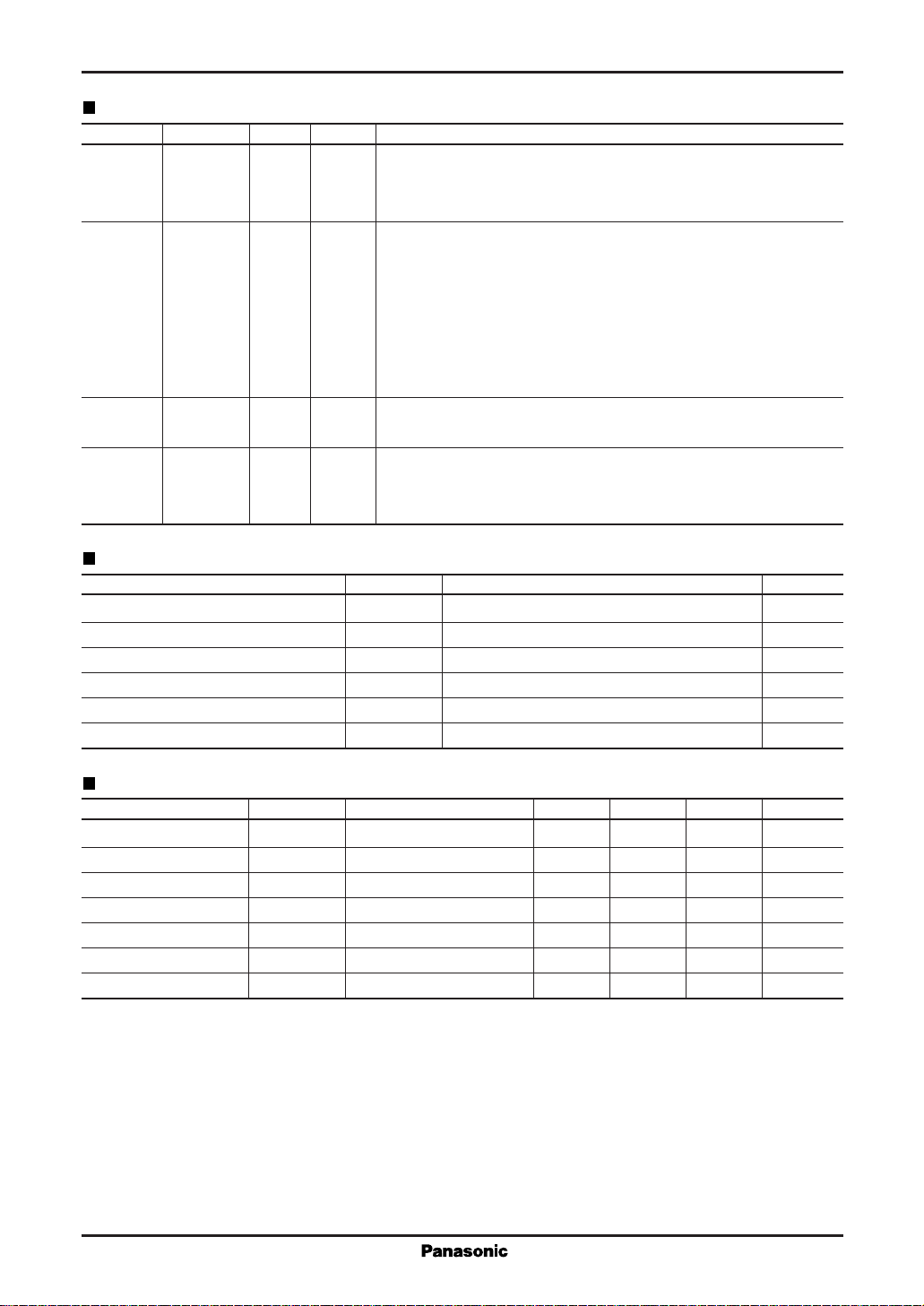
Pin No. Symbol I/O Level Function Description
124 RESET I TTL Reset
"H" level input from this pin initializes the chip. If the host is in a
i386 mode, the chip aligns the clock phase with this signal.
96 to 97 MA[1:0] I CMOS Host Type
During a reset, these pins select the host type.
MA[1:0] Host Type
0 0 ISA
0 1 386SX
1 0 386DX
1 1 486
126/125 TEST/ CMOS Chip Test Condition
MINTEST This pin selects the chip test mode.
1/128 XIN/ I/O Clock IN/OUT
XOUT These pins are the clock I/O pins. Connect them to a crystal
oscillator.
Absolute Maximum Ratings
Parameter Symbol Ratings Unit
Power supply voltage V
Input pin voltage V
Output pin voltage V
Power dissipaiton P
Operating ambient temperature T
Storage temperature T
DD
I
O
D
opr
stg
– 0.3 to +7.0 V
– 0.3 to VDD+0.3 V
– 0.3 to VDD+0.3 V
1000 mW
0 to +70 ˚C
– 55 to +150 ˚C
Recommended Operating Conditions
Parameter Symbol Conditions min typ max Unit
Power supply voltage V
DD
Ambient temperature Ta 0 70 ˚C
Rise time for input t
Fall time for input t
Oscillation frequency f
Operating frequency f
Operating frequency f
OSC
opr1
opr2
r
f
At self-excited operation 25 33 MHz
At self-excited operation 25 33 MHz
Using external input 0 33 MHz
4.75 5.00 5.25 V
0 150 ns
0 150 ns
Page 7
For Information Equipment MN89303A
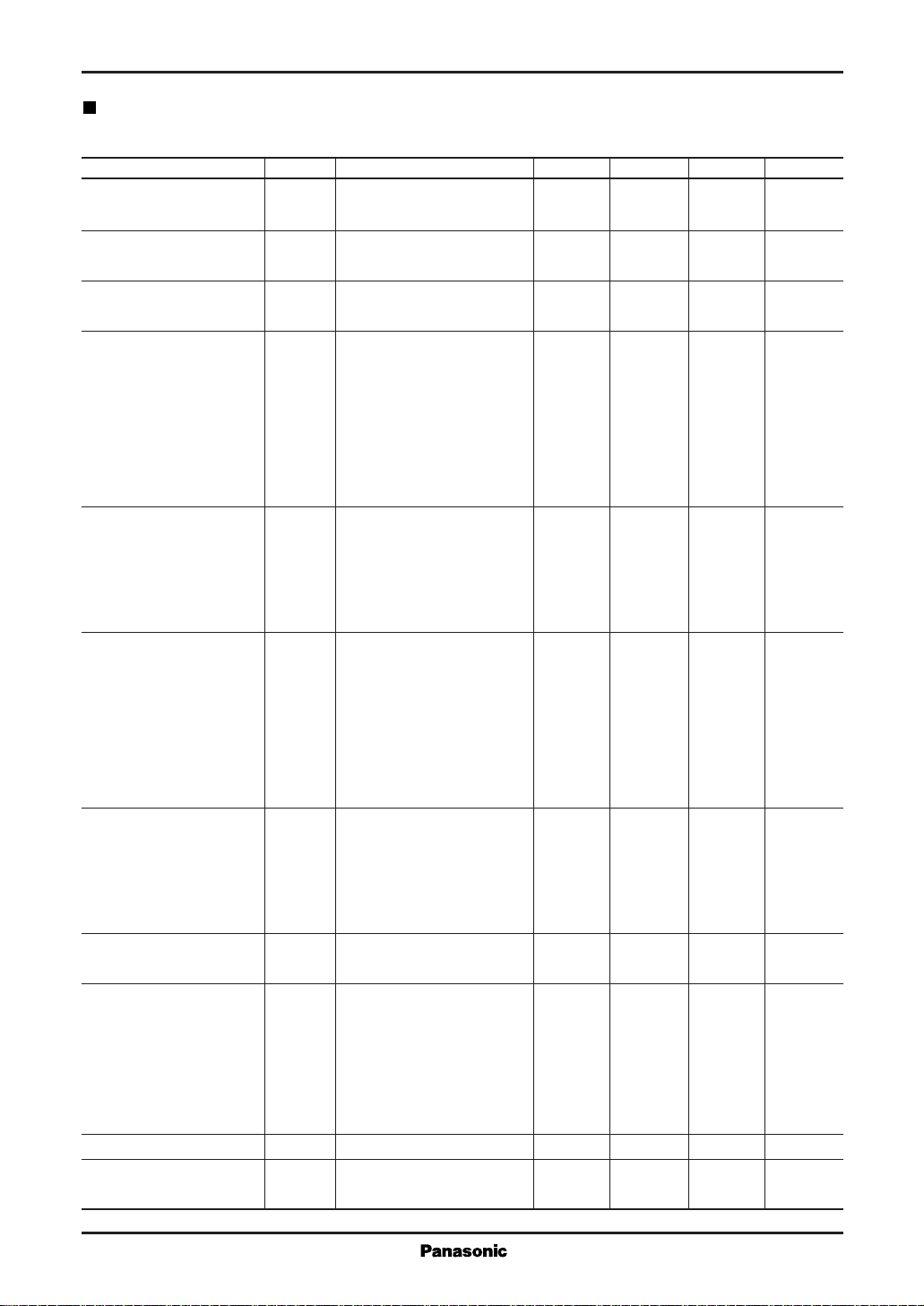
Electrical Characteristics
VDD=4.75 to 5.25V, VSS=0.00V, f=33MHz, Ta=0 to 70˚C
Parameter Symbol Conditions min typ max Unit
Power supply current I
during operation
Power supply current I
in the SUSPEND mode
Power supply current I
in the STANDBY mode
"H" level input voltage 1 V
TEST ,AEN ,SBHE ,
IOWR ,IORD ,SMEMW ,
SMEMR ,REFRESH ,
A21 to 20 ,SA19 to 0 ,
SD15 to 0 ,MD15 to 0 ,
BIOSEN ,IOCHRDY
"H" level input voltage 2 V
MINTEST ,RAS ,UCAS ,
LCAS ,BACKON ,
LCDON ,LOGICON ,
MA9 to 0
"L" level input voltage 1 V
TEST ,AEN ,SBHE ,
IOWR ,IORD ,SMEMW ,
SMEMR ,REFRESH ,
A21 to 20 ,SA19 to 0 ,
SD15 to 0 ,MD15 to 0 ,
BIOSEN ,IOCHRDY
"L" level input voltage 2 V
MINTESTRAS UCAS ,
LCAS ,BACKON ,
LCDON ,LOGICON ,
MA9 to 0
Input leakage current 1 I
TEST ,MINTEST
Input leakage current 2 I
AEN ,SBHE ,IOWR ,
IORD ,SMEMW ,
SMEMR ,REFRESH ,
A21 to 20 ,SA19 to 0 ,
RESET
Pull-down resistance R
Input threshold voltage V
RESET V
DD0
DD1
DD2
VI=VDD or VSS ,VDD=5.0V 120 mA
VI=VDD or VSS ,VDD=5.0V 15 mA
VI=VDD or VSS ,VDD=5.0V 40 mA
IH1
IH2
IL1
IL2
VI=VDD or V
LI1
VI=VDD or V
LI2
VI=VDD ,VDD=5.0V 12 30 75 kΩ
PD1
VDD=4.75 to 5.25V 1.0 V
tHL
tLH
SS
SS
2.0 V
V
× 0.7 V
DD
0 0.8 V
0V
1.8
DD
DD
× 0.3 V
DD
±20 µA
±10 µA
V
V
Page 8
MN89303A For Information Equipment
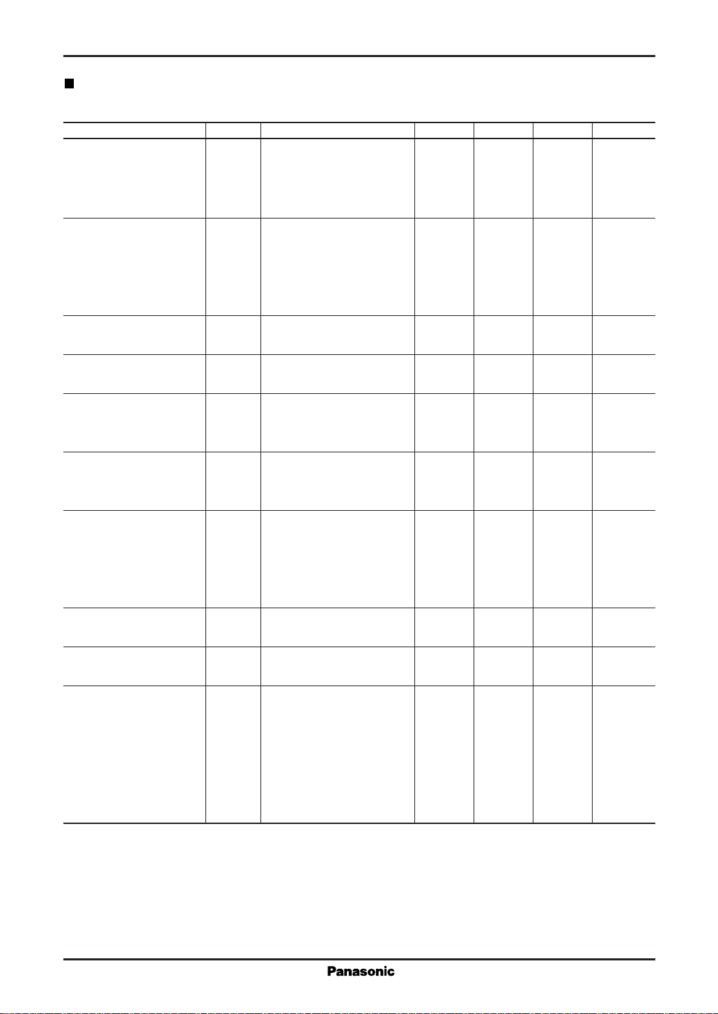
Electrical Characteristics (continued)
VDD=4.75 to 5.25V, VSS=0.00V, f=33MHz, Ta=0 to 70˚C
Parameter Symbol Conditions min typ max Unit
"H" level output voltage 1 V
OH1IO
BACKON ,LCDON , V
LOGICON ,SD15 to 0 ,
MD15 to 0 ,BIOSEN
"H" level output voltage 2 V
OH2IO
DCLK ,DISP ,LP ,FP , V
UD7 to 0 ,LD7 to 0 ,
WE ,MA9 to 0 ,RAS ,
UCAS ,LCAS
"H" level output voltage 3 V
OH3IO
IOCHRDY VI=VDD or V
"H" level output voltage 4 V
OH4IO
IOCS16 ,MEMCS16 VI=VDD or V
"L" level output voltage 1 V
OL1IO
BACKON ,LCDON , V
LOGICON
"L" level output voltage 2 V
OL2IO
SD15 to 0 ,MD15 to 0 , V
BIOSEN
"L" level output voltage 3 V
OL3IO
DCLK ,DISP ,LP ,FP , V
UD7 to 0 ,LD7 to 0 ,
WE ,MA9 to 0 ,RAS ,
UCAS ,LCAS
"L" level output voltage 4 V
OL4IO
IOCHRDY VI=VDD or V
"L" level output voltage 5 V
OL5IO
IOCS16 ,MEMCS16 VI=VDD or V
Output leakage current I
LO
IOCS16 ,BACKON , V
MA9 to 0 ,MEMCS16 , VO=VDD or V
UCAS ,LCAS ,RAS ,
LOGICON ,LCDON ,
SD15 to 0 ,MD15 to 0 ,
BIOSEN ,IOCHRDY
=–2.0mA VDD– 0.6 V
or V
I=VDD
SS
=–8.0mA VDD– 0.6 V
or V
I=VDD
SS
=–12.0mA VDD– 0.6 V
SS
=–16.0mA VDD– 0.6 V
SS
=2.0mA 0.4 V
or V
I=VDD
SS
=4.0mA 0.4 V
or V
I=VDD
SS
=0.8mA 0.4 V
or V
I=VDD
SS
=12.0mA 0.4 V
SS
=16.0mA 0.4 V
SS
VO=High-impedance state ±10 µA
or V
I=VDD
SS
SS
Page 9
For Information Equipment MN89303A
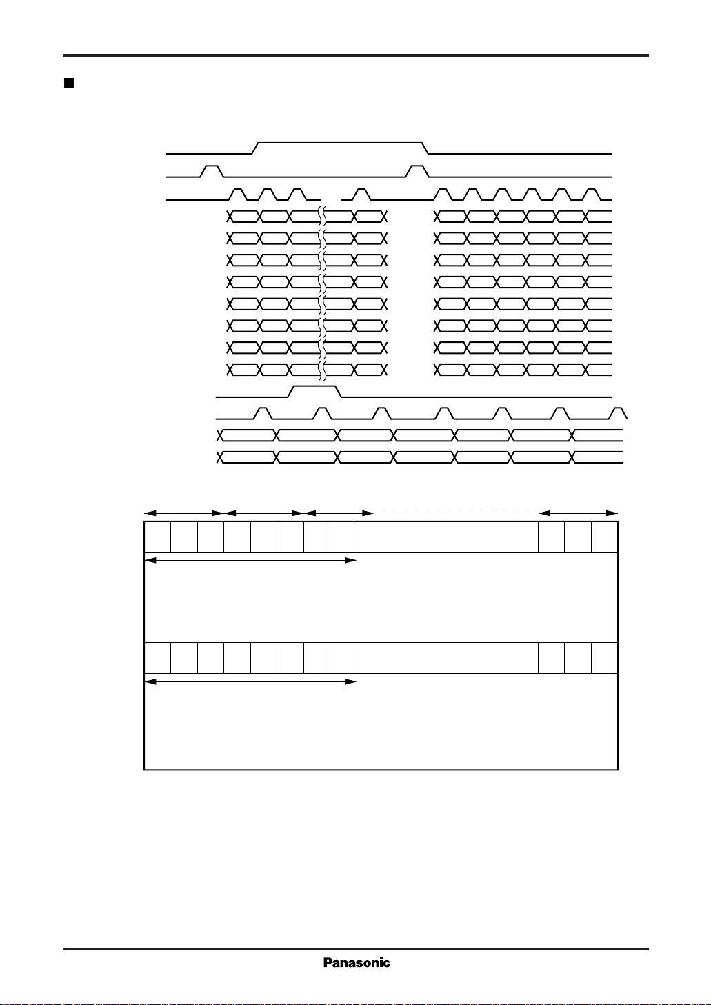
Timing Chart for LCD Panel Outputs
FP
LP
DCLK
R1 B3 R1 B3 G6G638LD7/UD7
G1 R4 G1 R4G4B6B638LD6/UD6
B1 G4 B1 R7R639LD5/UD5
R2 B4 R2 B4 G7G639LD4/UD4
G2 R5 G2 R5 B7B639LD3/UD3
B2 G5 B2 G5 R8R640LD2/UD2
R3 B5 R3 B5 G8G640LD1/UD1
G3
R6 G3 R6 B8B640LD0/UD0
FP
LP
UD
LD
240 lines 1 line 2 lines 3 lines 4 lines 5 lines
480 lines
241 lines 242 lines 243 lines 244 lines 245 lines
1 line
2 lines
·
·
·
·
·
240 lines
241 lines
242 lines
·
·
·
·
·
·
·
480 lines
1
R1
G1
UD7
R1
LD7G1LD6B1LD5R2LD4G2LD3B2LD2R3LD1G3LD0B3LD7
B1
UD6
UD5R2UD4G2UD3B2UD2R3UD1G3UD0B3UD7
First byte of data
First byte of data
2 3
Upper screen
Lower screen
R640
UD2
R640
LD2
640
G640
UD1
G640
LD1
B640
UD0
B640
LD0
Page 10
MN89303A For Information Equipment
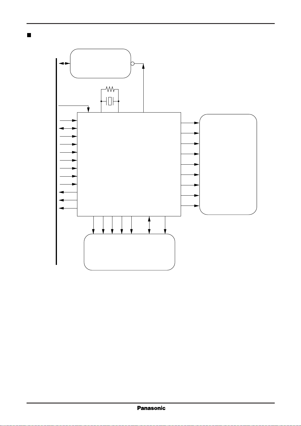
Application Circuit Example
RESET
BIOS
Address[21:0]
SD[15:0]
AEN
SBHE
IOWR
IORD
SMEMW
SMEMR
REFRESH
IOCHRDY
MEMCS16
IOCS16
CE (20)
XIN
MN89303A
BIOSENWELCAS
XOUT
UCAS
RAS
BIOSEN
MD[15:0]
UD[7:0]
LD[7:0]
BACKON
LCDON
LOGICON
DISP
DCLK
MA[9:0]
LCD
LP
FP
panel
ISA bus
4MDRAM
Page 11
For Information Equipment MN89303A
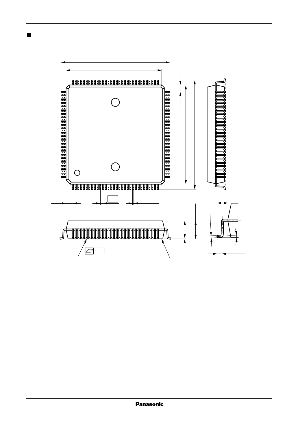
Package Dimensions (Unit: mm)
QFH128-P-1818
20.0±0.2
18.0
±0.2
96 65
97
(1.25)
64
(1.25)
18.0±0.2
20.0±0.2
33128
132
–0.05
+0.10
1.0±0.2
0.5
0.2±0.1
3.3±0.2
3.4±0.3
0.15
0.1
SEATING PLANE
0.1±0.1
0.5±0.2
0 to 10°
 Loading...