

Page 1
IC Card EEPROMs
MN63151
EEPROM for IC Cards
Overview
The MN63151 is an EEPROM for use in IC cards. It
features security features and an address specification
system using opcode input.
Low cost combined with high security makes the chips
ideal for use in prepaid cards and other types of IC cards.
Features
Easy-to-use control system
• Address specification system using opcode input
over a 3-wire interface (CLK, I/O, and RST)
• Automatic erasing and writing using a single 5 volt
power supply
Flexible memory-layout
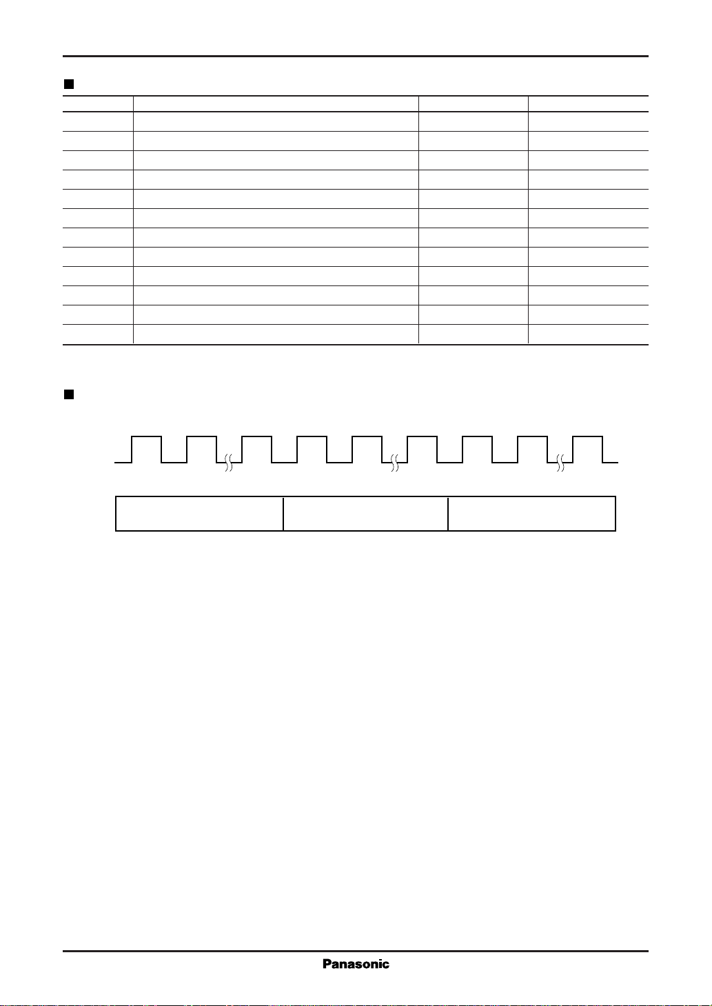
The memory is divided into 11 areas. Six areas containing 116 bytes are freely available.
Advanced security features
• Verification of IC card authenticity
The IC passes entered data through a random num-
ber generator circuit on its way to output to provide
a check of card validity.
• Protection against malicious experimentation
Four or more unsuccessful attempts to access the
IC card render it permanently unusable.
• Protection of individual memory areas on the card
Read or write access to a memory area requires
matches for both security and condition codes. There
is also a condition code for permanently disabling
re-writes.
• Mixed configuration of EPROM and EEPROM
Individual areas consist of EPROM or EEPROM.
High reliability
• Write cycles: 10,000 times
• Data storage interval: 10 years
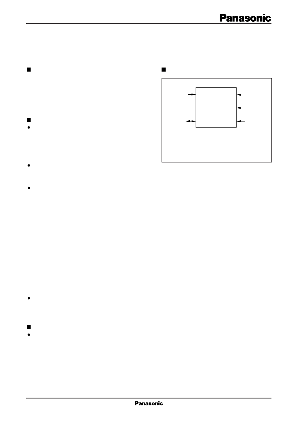
Pad Assignment
GND
I/O
Note: This product is sold as wafers.
1
2
(TOP VIEW)
5
V
DD
RST
4
CLK
3
Applications
IC cards
1
Page 2
MN63151 IC Card EEPROMs
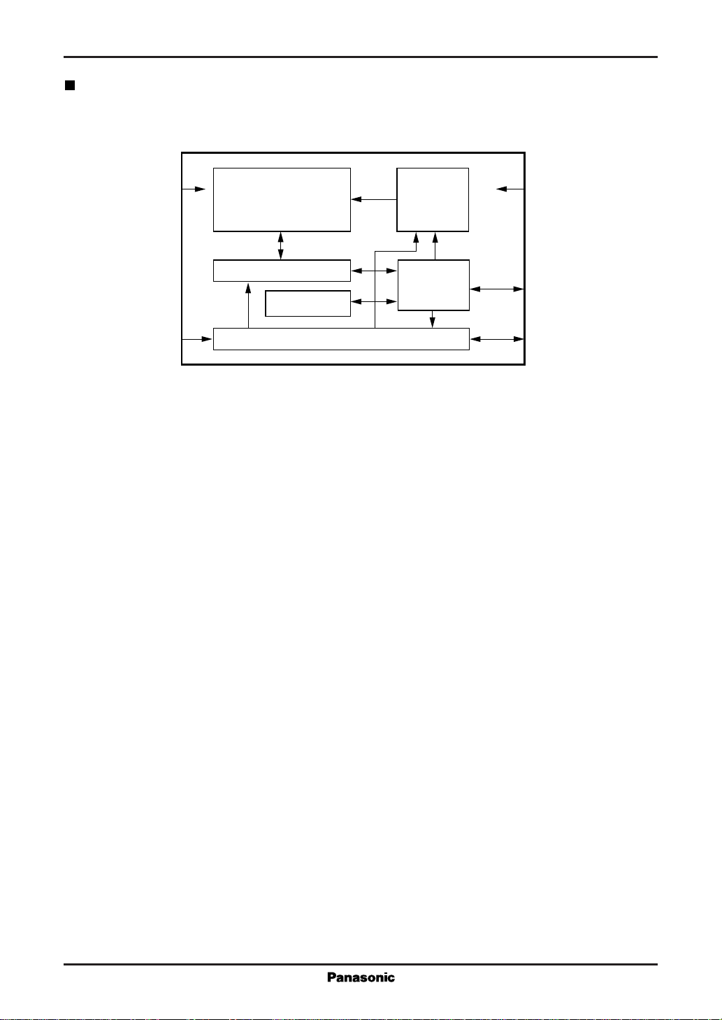
Block Diagram
GND
CLK
1
Memory (64 × 16)
Data register
Random number
generator
3
Mode decode-logic
Address
decoder
Data I/O
buffer
5
V
DD
2
I/O
4
RST
2
Page 3
IC Card EEPROMs MN63151
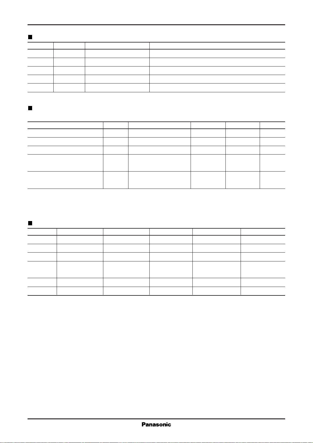
Pin Descriptions
Pin No. Symbol Pin Name I/O Direction
1 GND Ground I
2 I/O Data I/O I/O
3 CLK Clock I
4 RST Reset I
5VDDPower supply I
Electrical Characteristics
VCC=4.5 to 5.5V, Ta=–10˚C to +70˚C
Parameter Symbol Test Conditions min max Unit
Power supply voltage V
"L" level input leakage current I
"H" level input leakage current I
VCC power supply current I
CC
LIL
LIH
CC
VCC=5.5V
(during operation) CLK=800kHz
VCC power supply current I
SB
CLK="L"
(during standby) I/O="H"
Notes
: I/O pins use N-channel, open drain configuration.
1
: Input voltages, output voltages, and other items not listed above conform to ISO/IEC 7816-3.
2
4.5 5.5 V
–10 10 µA
–10 10 µA
— 5.45 mA
— 0.18 mA
Function Descriptions
Instruction Start Bit Operation Code Address Data Contents
READ 0 10 A5, A4–A
WRITE 0 01 A5, A4–A
0
0
VERIFY 0 11 001010 D0, D1–D
RNGEN 0 00 001010 D0, D1–D
RESET 0 11 111111 — Reset
EWEN 0 00 1xxxxx — Enable write
Note: x means "don’t care".
D0, D1–D
D0, D1–D
DO0, DO1–D
31
15
31
Verify code, generate
31
O31
Read
Write
Verify code
random number
3
Page 4
MN63151 IC Card EEPROMs
Memory Layout
Area Contents Number of Bits Memory Type
A Chip manufacturer's code 16 EPROM
B Card manufacturer's code 16 EPROM
C Spare area 1 32 EPROM
D Spare area 2 16 EEPROM
E Spare area 3 48 EPROM
F Spare area 4 16 EEPROM
G Security code 32 EEPROM
H Error counter 16 EEPROM
I1 Condition code 1 8 EPROM
I2 Condition code 2 8 EEPROM
J Application area 1 560 EPROM
K Application area 2 256 EEPROM
Timing Chart
CLK
I/O
Note: This product is sold as wafers.
Start bit and opcode Address Data
4
 Loading...