

Page 1
For Communications Equipment
MN6155
PLL LSI with Built-In Prescaler
Overview
The MN6155 is a CMOS LSI for a phase-locked loop
(PLL) frequency synthesizer with serial data parameter
input.
It consists of a two-coefficient prescaler, variable
frequency divider, phase comparator, and charge pump.
It offers high-speed operation on a low power supply
voltage (1.0 to 1.4 V) and low power consumption (1.65
mW for V
=1.1 V, FIN= RIN=90 MHz).
DD
Other features include intermittent operation by the
power save (PS) control signal and high-speed pull-in that
rapidly corrects the phase differences occurring at the start
of operation.
It also offers two choices for the reference signal: selfexcited operation using the built-in inverter amplifier or
use of an external, separately excited oscillator.
Features
Low power supply voltage:VDD=1.0 to 1.4V
Low power consumption: 1.65mW(VDD=1.10V,
F
=90MHz, RIN=90MHz)
IN
High-speed operation: FIN=90MHz, RIN=90MHz
(V
=1.1V)
DD
Frequency dividing ratios in reference frequency
dividing stage
6 to 131,070 for RSL at "H" level
(even number setting is available)
272 to 131,071 for RSL at "L" level
Frequency dividing ratios for comparator stage: 272
to 262,143
Power supply pin for built-in charge pump
V
=2.5 to 3.2V
CP
Output monitor pins for both comparator and reference
frequency dividing stages
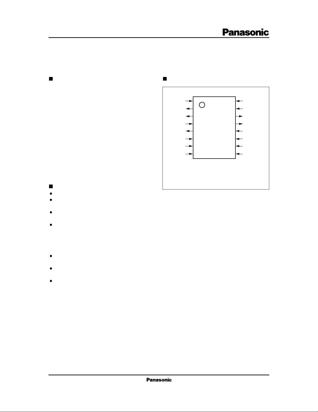
Pin Assignment
X
X
OUT
FV
V
D
V
V
F
DD
1
IN
2
3
4
5
OP
6
SS
7
CP
8
IN
SSOP016-P-0225
(TOP VIEW)
R
16
15
14
13
12
11
10
9
IN
RSL
LC
FR
PS
LE
DATA
CLK
Page 2
MN6155 For Communications Equipment
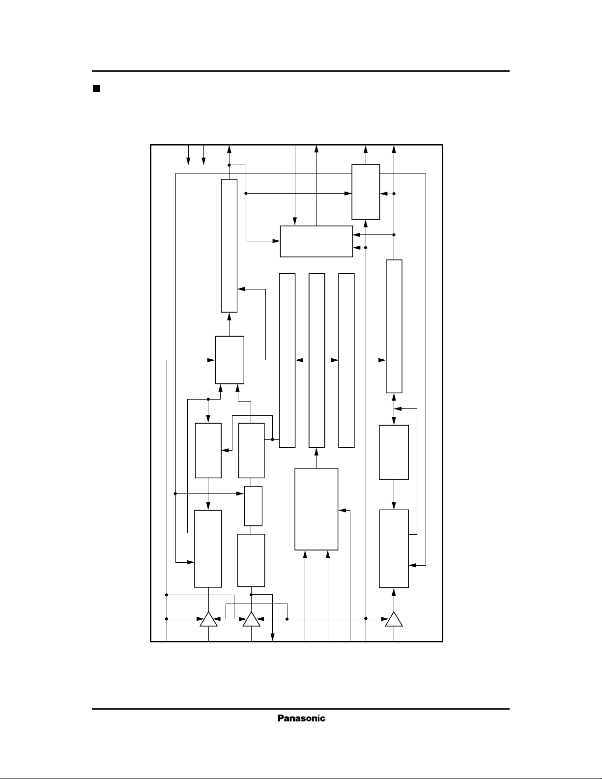
Block Diagram
DDVSS
V
4
FR
6
13
13-bit programmable counter
Switching
circuit
OP
VCPD
7
5
Phase comparator
17-bit latch
18-bit shift register
LC
14
Control
18-bit latch
FV
3
14-bit programmable counter
15
RSL
Swallow
counter
Prescaler and
phase adjustment
16
IN
R
3-bit counter
Phase
adjustment
Prescaler
1
2
IN
X
OUT
X
Data control
9
CLK
10
DATA
11
LE
12
PS
Swallow
counter
Prescaler and
phase adjustment
8
IN
F
Page 3
For Communications Equipment MN6155
Pin Descriptions
Pin No. Symbol Function Description
1X
2X
IN
OUT
3 FV Frequency divider output signal in comparator stage.
4VDDPower supply
5DOPLow-pass filter connection pin. Use a passive filter.
6VSSGround
7VCPPower supply pin for built-in charge pump
8FINFrequency divider input pin in comparator stage.
9 CLK Shift register clock input pin.
10 DATA Shift register data input pin.
11 LE Load enable signal input pin.
12 PS Power save control signal input pin.
13 FR Reference frequency divider output signal.
14 LC Charge pump control signal output pin.
15 RSL Reference signal selection pin.
16 R
IN
Crystal oscillator connection pins:
XIN =Oscillator circuit input pin;
is attached to a pull-up resistor when the PS or RSL pin is at "L" level.)
(X
IN
X
=Oscillator circuit output pin.
OUT
Phase comparator input monitor.
The chip latches data at the rising edge of the CLK signal.
The final two bits in the data select the write latch:
"11" for R-latch; "01" for N-latch.
This is the latch-write-enable signal. It is at "H" level for write.
"H" level input starts the frequency divider and places the chip in operational
mode. "L" level input places the chip in standby mode, which saves power.
The chip switches the internal charge pump output to the H-z state and the loop
is opened.
Phase comparator input monitor.
When frequency divider operation is stopped, this pin is at "L" level, the
internal charge pump output is in the high-impedance state, and the loop is opened.
"H" level selects self-excited oscillator (X
and X
IN
OUT
).
"L" level selects external oscillator (RIN).
External reference oscillation input pin.
This pin is attached to a pull-up resistor when the PS pin is at "L" level or the
RSL pin is at "H" level.
Page 4
MN6155 For Communications Equipment
MN6155 Frequency Dividing Data Settings
1) Comparator side frequency dividing data
FV = F
2) Reference side frequency dividing data
a) Low-speed operation (RSL pin at "H" level, using XIN)
FR = X
b) High-speed operation (RSL pin at "L" level, using R
FR =R
where
F
R
X
FV : Comparator frequency divider stage output frequency
FR : Reference frequency divider stage output frequency
N : Setting for 14-bit programmable counter on comparator side
A : Setting for 4-bit swallow counter on comparator side
R : Setting for 17-bit programmable counter on low-speed reference side
NR : Setting for 13-bit programmable counter on high-speed reference side
AR : Setting for 4-bit swallow counter on low-speed reference side
(Note that N should be greater than A; NR, greater than AR.)
÷ {(16 × N) + A}
IN
÷ R
IN
÷ {(16 × NR) + AR}
IN
: Comparator side frequency
IN
: High-speed reference frequency
IN
: Low-speed reference oscillator frequency
IN
)
IN
N-Side Latch Data
MSB
Programmable
counter setting (N)
R-Side Latch Data
Low-speed operation
MSB
High-speed operation
MSB
Programmable counter
setting (NR)
14 bits 4 bits
Swallow counter
setting (A)
17 bits
Programmable counter
setting (N)
13 bits
4 bits
Swallow counter
setting (AR)
LSB
LSB
LSB
Page 5
For Communications Equipment MN6155
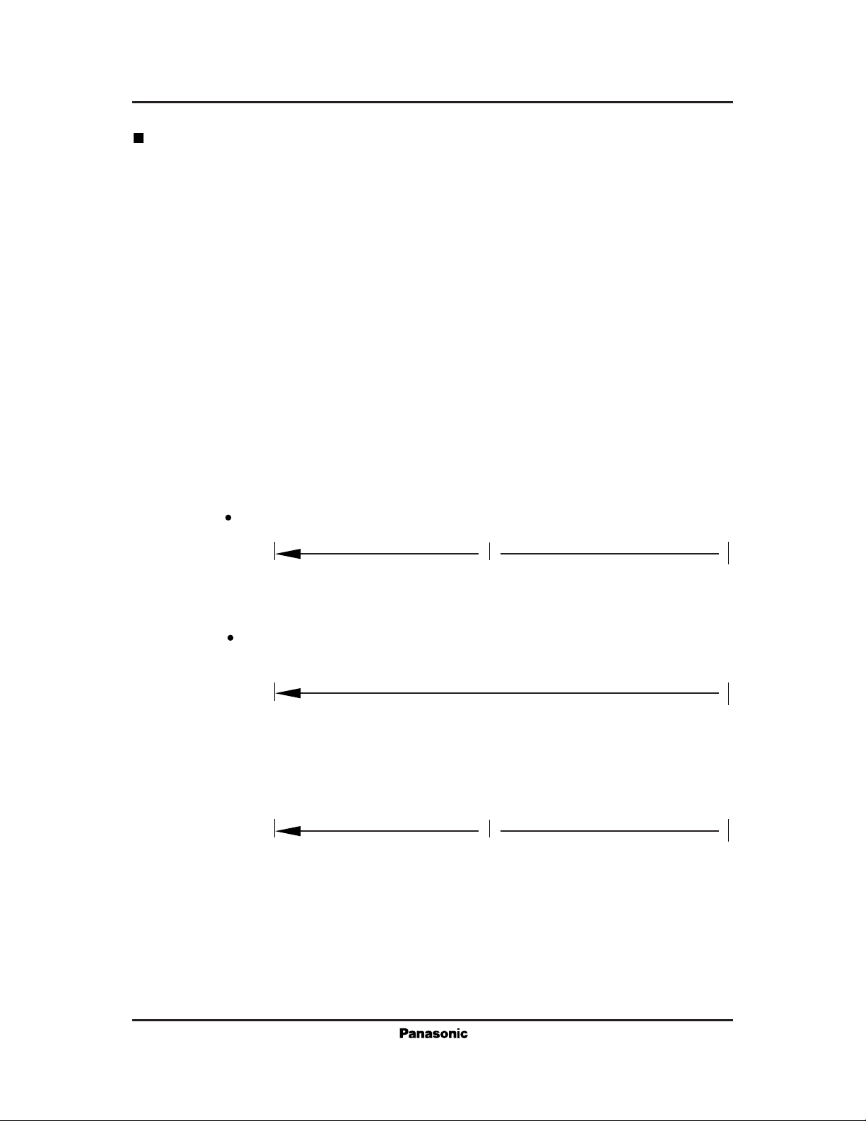
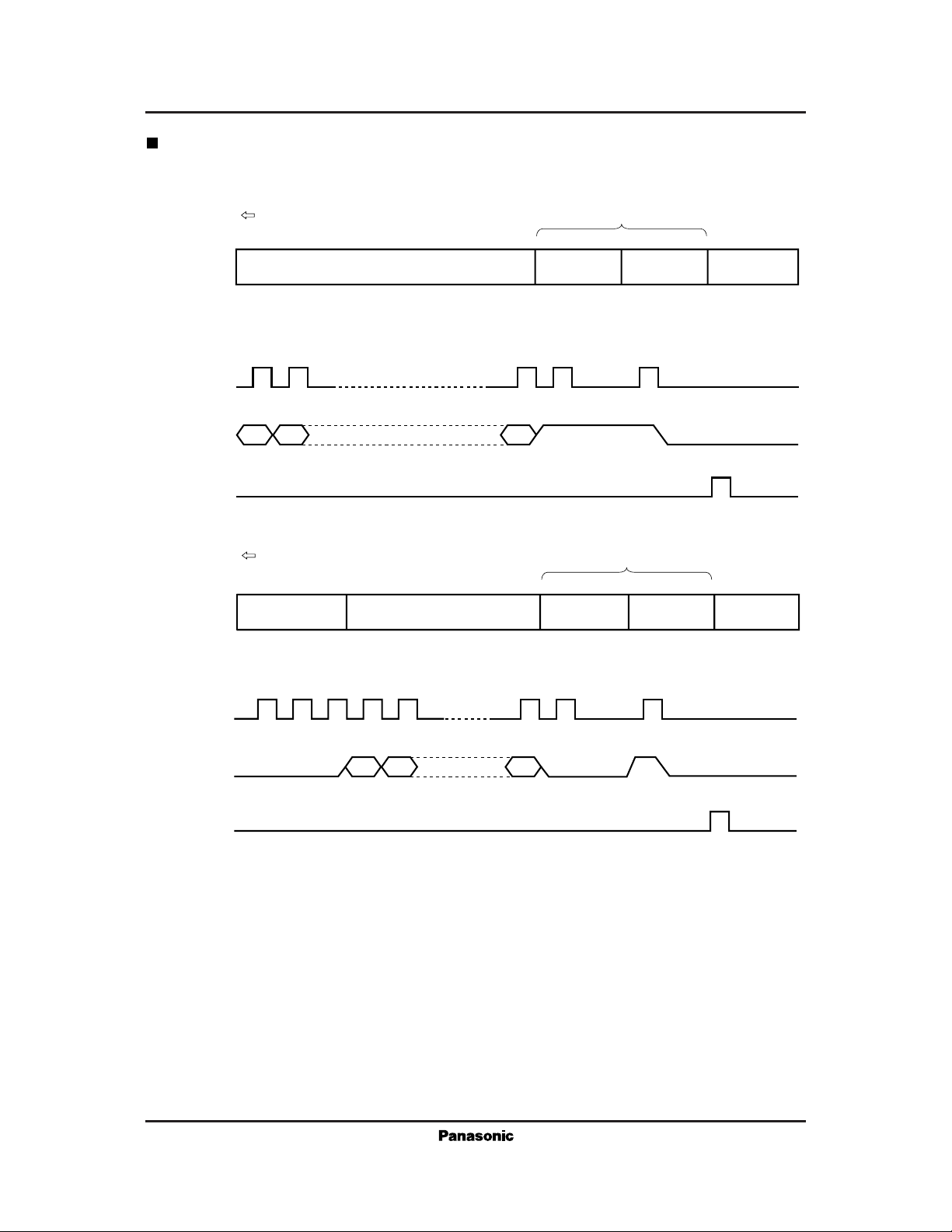
Note on Setting Frequency Dividing Data Input
1) Frequency dividing data input
(1) Reference side
Data input direction
MSB LSB
Control bits
1 2 17 18 19
CLK
DATA
MSB LSB
LE
(2) Comparating side
Data input direction
1
*
3-bit test data
3 bits "L" level
12345 2122 23
CLK
17-bit frequency dividing data
18-bit frequency dividing data
1 bit
Frequencey
dividing stage
selection "H" level
Control bits
1 bit 1 bit
Frequencey
dividing stage
selection "L" level
1 bit
Write selection
"H" level
Write selection
"H" level
"L"
"L"
DATA
MSB LSB
LE
Notes
1.*1: Preceding the input of the frequency dividing data for the comparating side, input test pattern consisting
of three "L" level bits to produce normal operation. Never use any other pattern.
2.
When the power is first applied, internal operation remains in an unstable state until data is written. To
eliminate the risk of excessive current consumption, keep the PS pin at "L" level.
3.
When the power is first applied, the data settings are indeterminate. Always write data to the chip before
starting operation.
4.
Enter the data to fill the entire latch:
Reference side: 19 bits (17 bits for the frequency divider setting and 2 for control bits)
Comparating side: 23 bits (3 bits for the test pattern, 18 bits for the frequency divider setting, and 2 for
control bits)
5.
Drive the LE pin at "L" level while writing the data.
6.
"H" level input from the LE pin causes the chip to read the data only when the CLK pin and the DATA pin
are both at "L" level.
7.
Writes are possible when the PS pin is either "H" or "L" level.
8.
Input the data MSB first.
9.
The data are inputted at the rising edge of the CLK signal.
Page 6
MN6155 For Communications Equipment
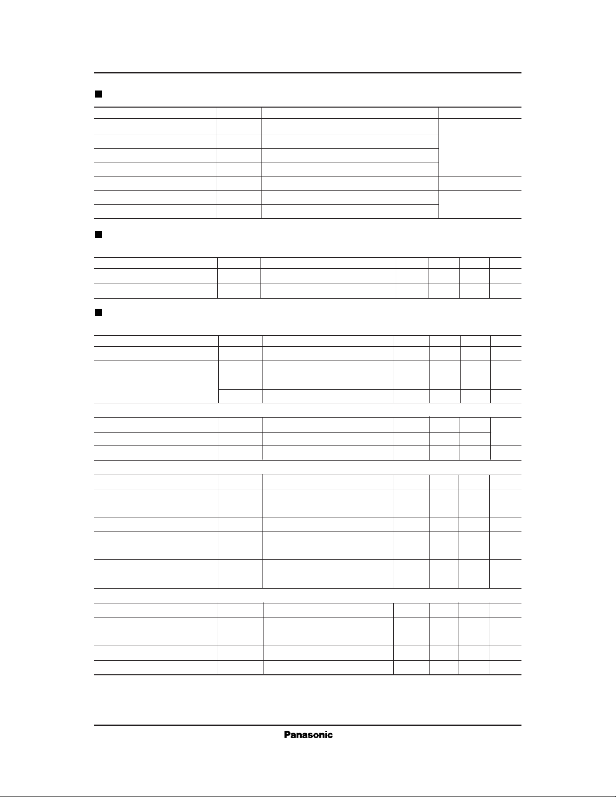
Absolute Maximum Ratings
Parameter Symbol Rating Unit
Power supply voltage V
Power supply voltage V
Input pin voltage V
Output pin voltage V
Power dissipation P
Operating ambient temperature T
Storage temperature T
DD
CP
I
O
D
opr
stg
Operating Conditions
VSS=0V, Ta=–10 to +60˚C
Parameter Symbol Test Conditions min typ max Unit
Power supply voltage V
Power supply voltage V
DD
CP
Electric Characteristics
VCP=2.5V, Ta=–10 to +60˚C
Parameter Symbol Test Conditions min typ max Unit
Power supply pin V
DD
I
DD
Power supply current PS="H", RSL="L"
I
Dstop
Input Pins CLK, DATA, LE, and PS VDD =1.0 to 1.4 V
"H" level input voltage V
"L" level input voltage V
Input leakage current I
Input Pins F
IN
, R
IN
Input voltage V
Input current I
Input leakage current I
Maximum operating frequency F
Minimum operating frequency F
Input Pin X
IN
V
=1.0 to 1.4V
DD
Input voltage V
Input current I
Input leakage current I
Maximum operating frequency X
IH
IL
LI
VDD=1.0 to 1.4V
IN
IF
LIF
INMAX
R
INMAX
INMIN
R
INMIN
IN
IX
LIX
INMAX
VDD=1.1V
FIN=90MHz, RIN=90MHz, 2.3 mA
PS="L" (Power Save operation) 3 µA
Pull-up resistor is present
(PS="L")
VIN=0 or VDD (PS="H") ±20 µA
VIN=0.4 V
VIN=0.4 V
Pull-up resistor is present
(PS="L")
VIN=0 or V
VIN=0.4 V
– 0.3 to +3.0
– 0.3 to +4.0
V
– 0.3 to VDD +0.3
SS
V
– 0.3 to VDD +0.3
SS
20 mW
–10 to +60
–55 to +125
p-p
p-p
DD
p-p
V
˚C
1.0 1.1 1.4 V
2.5 3.0 3.2 V
V
– 0.2 V
DD
V
SS
DD
0.2
±1.0 µA
0.4 V
–10 µA
90 MHz
1.0 MHz
0.4 V
– 0.1 –1.5 mA
5.0 µA
15 MHz
V
p-p
p-p
Page 7
For Communications Equipment MN6155
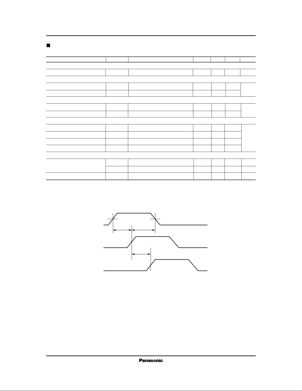
Electrical Characteristics (continued)
VCP=2.5V, Ta=–10 to +60˚C
Parameter Symbol Test Conditions min typ max Unit
Crystal Oscillator Pins XIN, X
Crystal oscillator frequency f
Output Pins FV, FR, LC V
DD
"H" level output voltage V
"L" level output voltage V
Output Pin X
OUT
VDD=1.0 to 1.4V
"H" level output voltage V
"L" level output voltage V
Output Pin D
OP
VDD=1.0 to 1.4V
"H" level output voltage I
"L" level output voltage I
Output leakage current I
Output leakage current I
VDD=1.0 to 1.4V
Setup time *
Hold time *
1
1
VDD=1.0 to 1.4V
OUT
Xtal
=1.0 to 1.4V
OH
OL
XOH
XOL
DOH
DOL
LOH
LOL
t
sul
t
su2
t
H
15 MHz
IOH= –10µA VDD– 0.3 V
IOL=10µA V
I
= –100µA VDD– 0.3 V
XOH
I
=100µA V
XOL
V
Dop=VCP
V
Dop
V
Dop=VCP
V
Dop
– 0.3V –100 µA
=0.3V –100
=0.0V –2.0
SS
SS
500 ns
500 ns
500 ns
0.3
0.3
2.0
DD
DD
V
V
Note*1: The following timing chart shows the setup and hold times.
DATA
CLK
LE
50%
t
su1
t
H
t
su2
Usage Note
Be particularly careful with this product as it is more sensitive on the static electricity damage than most of
our other products.
Page 8
MN6155 For Communications Equipment
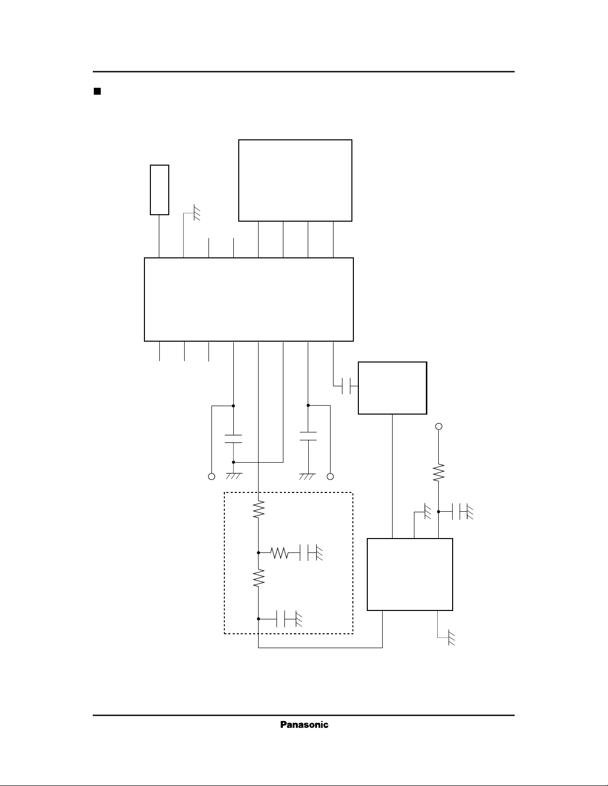
Application Circuit Example
eparately
excited
oscillator
S
Intermittent
operation
control
Frequency dividing
data input
Frequency dividing
data input
Frequency dividing
data input
16
IN
R
MN6155
INXOUT
X
1
15
2
RSL
14
3
LC
FV
13
4
V
FR
DD
12
11
PS
LE
OP
SS
D
V
5
6
10
DATA
V
7
9
CLK
CP
IN
F
VCO characteristics may necessitate design revisions.
1
*
8
Amplifier
=3V
CC
V
1000pF
0.1µF
0.1µF
=3V
CP
V
80 to 90MHz
390Ω
10µF
=1.0V to 1.4V
DD
V
10kΩ 100Ω
1µF
35kΩ
VCO
0.22µF
*1Loop filter
VF
V
CC
Page 9
For Communications Equipment MN6155
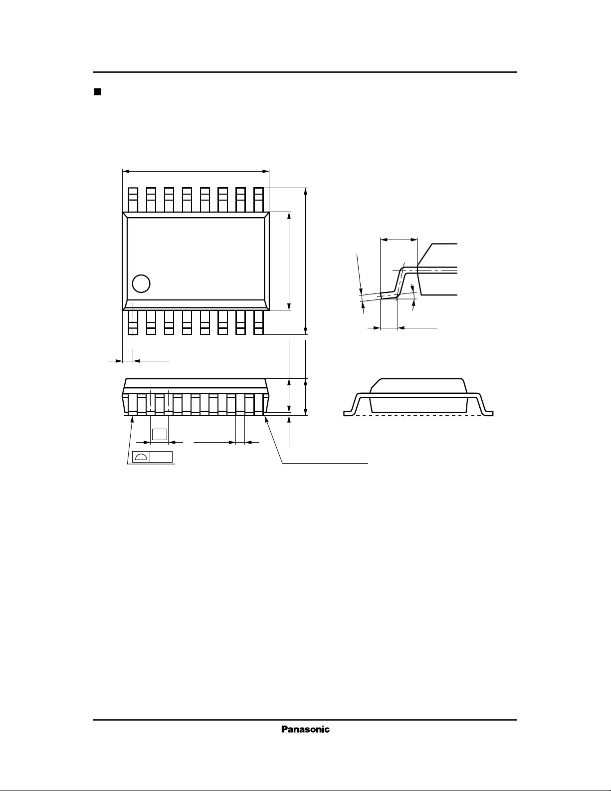
Package Dimensions (Unit: mm)
SSOP016-P-0225
6.5±0.2
16
9
1.0±0.1
0.05
-
4.3±0.2
6.3±0.2
+0.10
0.15
0 to 10°
0.5±0.1
1
(0.45)
0.8
0.15
0.35±0.10
8
1.45±0.200.1±0.1
SEATING PLANE
1.55±0.30
 Loading...