

Page 1
1
MOTOROLA
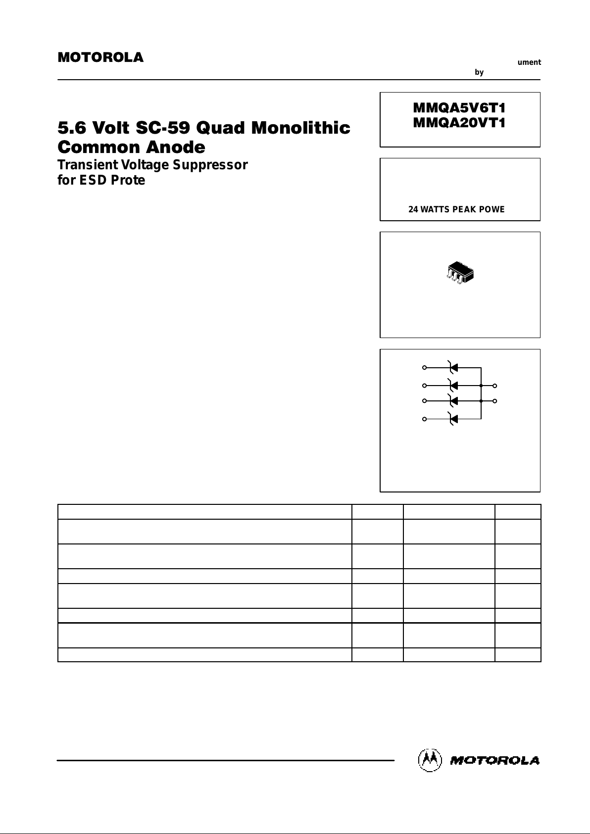
MMQA5V6T1 MMQA20VT1
Transient Voltage Suppressor
for ESD Protection
This quad monolithic silicon voltage suppressor is designed for applications
requiring transient overvoltage protection capability. It is intended for use in
voltage and ESD sensitive equipment such as computers, printers, business
machines, communication systems, medical equipment, and other applications. Its quad junction common anode design protects four separate lines
using only one package. These devices are ideal for situations where board
space is at a premium.
Specification Features:
• SC-59 Package Allows Four Separate Unidirectional Configurations
• Peak Power — 24 Watts @ 1.0 ms (Unidirectional), per Figure 7 Waveform
• Maximum Clamping Voltage @ Peak Pulse Current
• Low Leakage < 2.0 µA
• ESD Rating of Class N (exceeding 16 kV) per the Human Body Model
Mechanical Characteristics:
• Void Free, Transfer-Molded, Thermosetting Plastic Case
• Corrosion Resistant Finish, Easily Solderable
• Package Designed for Optimal Automated Board Assembly
• Small Package Size for High Density Applications
• Available in 8 mm Tape and Reel
Use the Device Number to order the 7 inch/3,000 unit reel. Replace
with “T3” in the Device Number to order the 13 inch/10,000 unit reel.
THERMAL CHARACTERISTICS
(TA = 25°C unless otherwise noted)
Characteristic
Symbol Value Unit
Peak Power Dissipation @ 1.0 ms (1)
@ TA ≤ 25°C
P
pk
24 Watts
Total Power Dissipation on FR-5 Board (2) @ TA = 25°C
Derate above 25°C
°PD° °225
1.8
°mW°
mW/°C
Thermal Resistance Junction to Ambient R
θJA
556 °C/W
Total Power Dissipation on Alumina Substrate (3) @ TA = 25°C
Derate above 25°C
°PD° °300
2.4
°mW
mW/°C
Thermal Resistance Junction to Ambient R
θJA
417 °C/W
Junction and Storage Temperature Range T
J
T
stg
°– 55 to +150° °C
Lead Solder Temperature — Maximum (10 Second Duration) T
L
260 °C
1. Non-repetitive current pulse per Figure 7 and derate above TA = 25°C per Figure 8.
2. FR-5 = 1.0 x 0.75 x 0.62 in.
3. Alumina = 0.4 x 0.3 x 0.024 in., 99.5% alumina
4. Other voltages are available
Thermal Clad is a trademark of the Bergquist Company
Preferred devices are Motorola recommended choices for future use and best overall value.
SEMICONDUCTOR TECHNICAL DATA
Order this document
by MMQA5V6T1/D
Motorola, Inc. 1996
Rev 3
SC-59 QUAD
TRANSIENT VOLTAGE
SUPPRESSOR
5.6 VOLTS (4)
24 WATTS PEAK POWER
CASE 318F-01
STYLE 1
SC-59 PLASTIC
4 5
6
Motorola Preferred Devices
PIN 1. CATHODE
2. ANODE
3. CATHODE
4. CATHODE
5. ANODE
6. CATHODE
1
2
3
1
2
3
4
5
6
Page 2

MOTOROLA
2
MMQA5V6T1 MMQA20VT1
ELECTRICAL CHARACTERISTICS (T
A
= 25°C unless otherwise noted)
UNIDIRECTIONAL (Circuit tied to pins 1, 2, and 5; Pins 2, 3, and 5; Pins 2, 4, and 5; or Pins 2, 5, and 6) (V
F
= 0.9 V Max @ IF = 10 mA)
Breakdown Voltage
Max Reverse
Leakage Current
Max Zener Impedance (5)
Max
Reverse
Max Reverse
Voltage @
Maximum
VZT(3)
(V)
@ I
ZT
IR @ VR
ZZT @ IZT
Surge
Current
I
RSM(4)
I
RSM
(4)
(Clamping
Voltage)
Temperature
Coefficient of
V
Z
Min Nom Max
(mA)
1
(µA) (V)
(Ω) (mA)
I
RSM(4)
(A)
V
RSM
(V)
(mV/°C)
5.32 5.6 5.88 1.0 2.0 3.0 400 3.0 8.0 1.26
19 20 21 1.0 0.1 15 125 0.84 28.6 20.07
(3) VZ measured at pulse test current IT at an ambient temperature of 25°C.
(4) Surge current waveform per Figure 5 and derate per Figure 6.
(5) ZZT is measured by dividing the AC voltage drop across the device by the AC current supplied. The specfied limits are I
Z(AC)
= 0.1 I
Z(DC)
, with AC frequency = 1 kHz.
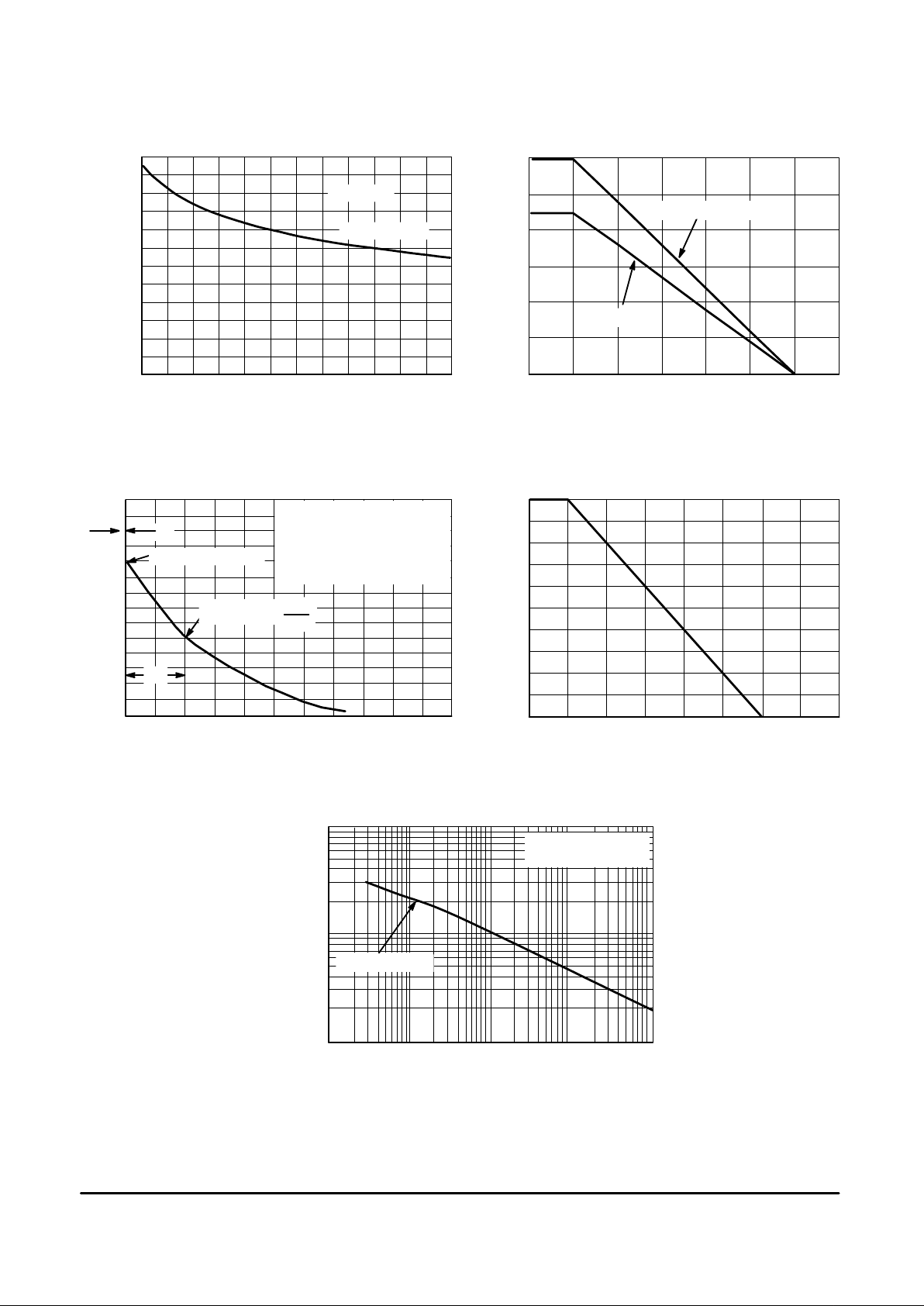
Typical Characteristics
– 50 50 100 150
8
7
6
5
4
V ,
Z
BREAKDOWN VOLTAGE (VOLTS)
23
17
TA, AMBIENT TEMPERATURE (
°
C)
Figure 1. Typical Breakdown Voltage
versus Temperature
Figure 2. Typical Breakdown Voltage
versus Temperature
0 2 4 6 8 10 14 16
70
60
50
40
30
20
0
C, CAPACITANCE (pF)
0 – 40 25 150
TA, AMBIENT TEMPERATURE (
°
C)
REVERSE VOLTAGE (V)
VZ @ I
T
MMQA5V6T1
22
21
20
19
18
MMQA20VT1
10000
1000
100
TA, AMBIENT TEMPERATURE (
°
C)
I
R,
REVERSE LEAKAGE CURRENT (nA)
– 50 50 100 1500
Figure 3. Typical Leakage Current
versus Temperature
Figure 4. Typical Capacitance versus
Reverse Voltage
10
12
MMQA20VT1
UNIDIRECTIONAL
V ,
Z
BREAKDOWN VOLTAGE (VOLTS)
0
UNIDIRECTIONAL
Page 3
3
MOTOROLA
MMQA5V6T1 MMQA20VT1
Typical Characteristics
0 1 1.5 3
300
Figure 5. Typical Capacitance versus
Reverse Voltage
0 25 50 75 100 125 150 175
300
250
200
150
100
50
0
Figure 6. Steady State Power Derating Curve
P
D
, POWER DISSIPATION (mW)
0.5
REVERSE VOLTAGE (V)
TA, AMBIENT TEMPERATURE (
°
C)
FR-5 BOARD
ALUMINA SUBSTRATE
C, CAPACITANCE (pF)
2 2.5
275
250
225
200
175
150
125
100
75
50
25
0
UNIDIRECTIONAL
MMQA5V6T1
VALUE (%)
100
50
0
0 1 2 3 4
t, TIME (ms)
Figure 7. Pulse Waveform
t
r
t
P
100
90
80
70
60
50
40
30
20
10
0
0 25 50 75 100 125 150 175 200
TA, AMBIENT TEMPERATURE (
°
C)
Figure 8. Pulse Derating Curve
PEAK PULSE DERATING IN % OF PEAK POWER
OR CURRENT @ T
A
= 25
C
°
Figure 9. Maximum Non-repetitive Surge
Power, Ppk versus PW
Ppk PEAK SURGE POWER (W)
0.1 1.0 10 100 1000
1.0
10
100
Power is defined as V
RSM
x IZ(pk) where V
RSM
is the clamping voltage at IZ(pk).
PW, PULSE WIDTH (ms)
PULSE WIDTH (tP) IS DEFINED
AS THAT POINT WHERE THE
PEAK CURRENT DECAYS TO 50%
OF I
RSM
.
tr
≤
10 µs
HALF VALUE—
I
RSM
2
PEAK VALUE—I
RSM
UNIDIRECTIONAL
RECTANGULAR
WAVEFORM, TA = 25
°
C
Page 4

MOTOROLA
4
MMQA5V6T1 MMQA20VT1
TYPICAL COMMON ANODE APPLICATIONS
A quad junction common anode design in a SC-59 package protects four separate lines using only one package.
This adds flexibility and creativity to PCB design especially
when board space is at a premium. Two simplified examples
of MMQA5V6T1 and MMQA20VT1 applications are illustrated below.
MMQA5V6T1
MMQA20VT1
KEYBOARD
TERMINAL
PRINTER
ETC.
FUNCTIONAL
DECODER
I/O
A
MMQA5V6T1
MMQA20VT1
GND
Computer Interface Protection
B
C
D
Microprocessor Protection
I/O
RAM ROM
CLOCK
CPU
CONTROL BUS
ADDRESS BUS
DATA BUS
GND
V
GG
V
DD
Page 5

5
MOTOROLA
MMQA5V6T1 MMQA20VT1
INFORMATION FOR USING THE SC-59 6 LEAD SURFACE MOUNT PACKAGE
MINIMUM RECOMMENDED FOOTPRINT FOR SURFACE MOUNTED APPLICATIONS
Surface mount board layout is a critical portion of the total
design. The footprint for the semiconductor packages must
be the correct size to ensure proper solder connection inter-
face between the board and the package. With the correct
pad geometry, the packages will self-align when subjected to
a solder reflow process.
inches
mm
SC-59 6 LEAD
0.028
0.7
0.074
1.9
0.037
0.95
0.037
0.95
0.094
2.4
0.039
1.0
SC-59 6 LEAD POWER DISSIPATION
The power dissipation of the SC-59 6 Lead is a function of
the pad size. This can vary from the minimum pad size for
soldering to a pad size given for maximum power dissipation.
Power dissipation for a surface mount device is determined
by T
J(max)
, the maximum rated junction temperature of the
die, R
θJA
, the thermal resistance from the device junction to
ambient, and the operating t emperature, TA. Using t he
values provided o n the data sheet for the SC-59 6 Lead
package, PD can be calculated as follows:
PD =
T
J(max)
– T
A
R
θJA
The values for the equation are found in the maximum
ratings table on the data sheet. Substituting these values into
the equation for an ambient temperature TA of 25°C, one can
calculate the power dissipation of the device which in this
case is 225 milliwatts.
PD =
150°C – 25°C
556°C/W
= 225 milliwatts
The 556°C/W for the SC-59 6 Lead package assumes the
use of the recommended footprint on a glass epoxy printed
circuit board to achieve a power dissipation of 225 milliwatts.
There a re other alternatives t o achieving higher power
dissipation from the SC-59 6 Lead package. Another alternative would be to use a ceramic substrate or an aluminum
core board such as Thermal Clad. Using a board material
such as Thermal Clad, an aluminum core board, the power
dissipation can be doubled using the same footprint.
SOLDER STENCIL GUIDELINES
Prior to placing surface mount components onto a printed
circuit board, solder paste must be a pplied to t he pads.
Solder stencils are used to screen the optimum amount.
These stencils are typically 0.008 inches thick and may be
made of brass or stainless steel. For packages such as the
SC-59, SC-59 6 Lead, SC-70/SOT-323, SOD-123, SOT-23,
SOT-143, SOT-223, SO-8, SO-14, SO-16, and SMB/SMC
diode packages, the stencil opening should be the same as
the pad size or a 1:1 registration.
SOLDERING PRECAUTIONS
The melting temperature of solder is higher than the rated
temperature of the device. When the entire device is heated
to a high temperature, failure to complete soldering within a
short t ime could result i n device f ailure. Therefore, the
following items should always be observed in order to minimize the thermal stress to which the devices are subjected.
• Always preheat the device.
• The delta temperature between the preheat and
soldering should be 100°C or less.*
• When preheating and soldering, the temperature of the
leads and the case must not exceed the maximum
temperature ratings as shown on the data sheet. When
using infrared heating with the reflow soldering method,
the difference should be a maximum of 10°C.
* Soldering a device without preheating can cause excessive
thermal shock and stress which can result in damage to the
device.
Page 6

MOTOROLA
6
MMQA5V6T1 MMQA20VT1
• The soldering temperature and time should not exceed
260°C for more than 10 seconds.
• When shifting from preheating to soldering, the
maximum temperature gradient should be 5°C or less.
• After soldering has been completed, the device should
be allowed to cool naturally for at least three minutes.
Gradual cooling should be used since the use of forced
cooling will increase the temperature gradient and will
result in latent failure due to mechanical stress.
• Mechanical stress or shock should not be applied during
cooling.
TYPICAL SOLDER HEATING PROFILE
For any given circuit board, there will be a group of control
settings that will give the desired heat pattern. The operator
must set temperatures for several heating zones and a figure
for belt speed. Taken together, these control settings make
up a heating “profile” for that particular circuit board. On
machines controlled by a computer, the computer remembers these profiles from one operating session to the next.
Figure 8 s hows a t ypical h eating profile f or use w hen
soldering a surface mount device to a printed circuit board.
This profile will vary among soldering systems, but it is a
good starting point. Factors that can affect the profile include
the type of soldering system in use, density and types of
components on the board, type of solder used, and the type
of board or substrate material being used. This profile shows
temperature versus time. The line on the graph shows the
actual temperature that might be experienced on the surface
of a test board at or near a central solder joint. The two
profiles are based on a high density and a low density board.
The Vitronics SMD310 convection/infrared reflow soldering
system was used to generate this profile. The type of solder
used w as 62/36/2 Tin Lead Silver with a m elting p oint
between 177 –189°C. When this type of furnace is used for
solder reflow work, the circuit boards and solder joints tend to
heat first. The components on the board are then heated by
conduction. The circuit board, because it has a large surface
area, absorbs the thermal energy more efficiently, then
distributes this energy to the components. Because of this
effect, the m ain body of a component may be u p to 30
degrees cooler than the adjacent solder joints.
STEP 1
PREHEAT
ZONE 1
“RAMP”
STEP 2
VENT
“SOAK”
STEP 3
HEATING
ZONES 2 & 5
“RAMP”
STEP 4
HEATING
ZONES 3 & 6
“SOAK”
STEP 5
HEATING
ZONES 4 & 7
“SPIKE”
STEP 6
VENT
STEP 7
COOLING
200
°
C
150
°
C
100
°
C
50°C
TIME (3 TO 7 MINUTES TOTAL)
T
MAX
SOLDER IS LIQUID FOR
40 TO 80 SECONDS
(DEPENDING ON
MASS OF ASSEMBLY)
205
°
TO 219°C
PEAK AT
SOLDER JOINT
DESIRED CURVE FOR LOW
MASS ASSEMBLIES
100°C
150°C
160
°
C
170°C
140
°
C
Figure 10. Typical Solder Heating Profile
DESIRED CURVE FOR HIGH
MASS ASSEMBLIES
Page 7

7
MOTOROLA
MMQA5V6T1 MMQA20VT1
OUTLINE DIMENSIONS
CASE 318F-01
ISSUE A
SC-59 6 LEAD
NOTES:
1. DIMENSIONING AND TOLERANCING PER ANSI
Y14.5M, 1982.
2. CONTROLLING DIMENSION: INCH.
3. MAXIMUM LEAD THICKNESS INCLUDES LEAD
FINISH THICKNESS. MINIMUM LEAD THICKNESS
IS THE MINIMUM THICKNESS OF BASE
MATERIAL.
STYLE 1:
PIN 1. CATHODE
2. ANODE
3. CATHODE
4. CATHODE
5. ANODE
6. CATHODE
MIN MINMAX MAX
INCHES MILLIMETERS
DIM
A
B
C
D
G
H
J
K
L
M
S
2.70
1.30
1.00
0.35
0.85
0.013
0.10
0.20
1.25
0
_
2.50
3.10
1.70
1.30
0.50
1.05
0.100
0.26
0.60
1.65
10
_
3.00
0.1063
0.0512
0.0394
0.0138
0.0335
0.0005
0.0040
0.0079
0.0493
0
_
0.0985
0.1220
0.0669
0.0511
0.0196
0.0413
0.0040
0.0102
0.0236
0.0649
10
_
0.1181
A
G
S
L
D
H
C
K
J
B
0.05 (0.002)
M
1 2 3
456
Page 8

MOTOROLA
8
MMQA5V6T1 MMQA20VT1
Motorola reserves the right to make changes without further notice to any products herein. Motorola makes no warranty , representation or guarantee regarding
the suitability of its products for any particular purpose, nor does Motorola assume any liability arising out of the application or use of any product or circuit,
and specifically disclaims any and all liability, including without limitation consequential or incidental damages. “T ypical” parameters can and do vary in different
applications. All operating parameters, including “T ypicals” must be validated for each customer application by customer’s technical experts. Motorola does
not convey any license under its patent rights nor the rights of others. Motorola products are not designed, intended, or authorized for use as components in
systems intended for surgical implant into the body, or other applications intended to support or sustain life, or for any other application in which the failure of
the Motorola product could create a situation where personal injury or death may occur. Should Buyer purchase or use Motorola products for any such
unintended or unauthorized application, Buyer shall indemnify and hold Motorola and its officers, employees, subsidiaries, affiliates, and distributors harmless
against all claims, costs, damages, and expenses, and reasonable attorney fees arising out of, directly or indirectly, any claim of personal injury or death
associated with such unintended or unauthorized use, even if such claim alleges that Motorola was negligent regarding the design or manufacture of the part.
Motorola and are registered trademarks of Motorola, Inc. Motorola, Inc. is an Equal Opportunity/Affirmative Action Employer.
How to reach us:
USA /EUROPE: Motorola Literature Distribution; JAPAN: Nippon Motorola Ltd.; Tatsumi–SPD–JLDC, Toshikatsu Otsuki,
P.O. Box 20912; Phoenix, Arizona 85036. 1–800–441–2447 6F Seibu–Butsuryu–Center, 3–14–2 Tatsumi Koto–Ku, Tokyo 135, Japan. 03–3521–8315
MFAX: RMFAX0@email.sps.mot.com – TOUCHTONE (602) 244–6609 HONG KONG: Motorola Semiconductors H.K. Ltd.; 8B Tai Ping Industrial Park,
INTERNET: http://Design–NET.com 51 Ting Kok Road, Tai Po, N.T., Hong Kong. 852–26629298
MMQA5V6T1/D
*MMQA5V6T1/D*
◊
 Loading...