

Page 1
1
Motorola IGBT Device Data
N–Channel Enhancement–Mode Silicon Gate
This IGBT contains a built–in free wheeling diode and a gate
protection zener diodes. Fast switching characteristics result in
efficient operation at higher frequencies. This device is ideally
suited for high frequency electronic ballasts.
• Built–In Free Wheeling Diode
• Built–In Gate Protection Zener Diodes
• Industry Standard Package (SOT223)
• High Speed E
off
: Typical 6.5 mJ @ IC = 0.3 A; TC = 125°C and
dV/dt = 1000 V/ms
• Robust High Voltage Termination
• Robust Turn–Off SOA
MAXIMUM RATINGS
(TJ = 25°C unless otherwise noted)
Parameters Symbol Value Unit
Collector–Emitter Voltage V
CES
600 Vdc
Collector–Gate Voltage (RGE = 1.0 MΩ) V
CGR
600 Vdc
Gate–Emitter Voltage — Continuous V
CGR
±15 Vdc
Collector Current — Continuous @ TC = 25°C
Collector Current — Continuous @ TC = 90°C
Collector Current — Repetitive Pulsed Current (1)
I
C25
I
C90
I
CM
0.5
0.3
2.0
Adc
Total Device Dissipation @ TC = 25°C P
D
1.0 Watt
Operating and Storage Junction Temperature Range TJ, T
stg
–55 to 150 °C
Thermal Resistance — Junction to Case – IGBT
Thermal Resistance — Junction to Ambient
R
θJC
R
θJA
30
150
°C/W
Maximum Lead Temperature for Soldering Purposes, 1/8″ from case for 5 seconds T
L
260 °C
UNCLAMPED DRAIN–TO–SOURCE AVALANCHE CHARACTERISTICS (T
C
≤ 150°C)
Single Pulse Drain–to–Source Avalanche
Energy – Starting @ TC = 25°C
Energy – Starting @ TC = 125°C
VCE = 100 V , VGE = 15 V, Peak IL = 2.0 A, L = 3.0 mH, RG = 25
W
E
AS
125
40
mJ
(1) Pulse width is limited by maximum junction temperature repetitive rating.
Designer’s Data for “Worst Case” Conditions— The Designer’s Data Sheet permits the design of most circuits entirely from the information presented. SOA Limit
curves — representing boundaries on device characteristics — are given to facilitate “worst case” design.
Designer’s is a trademark of Motorola, Inc.
REV 2
Order this document
by MMG05N60D/D
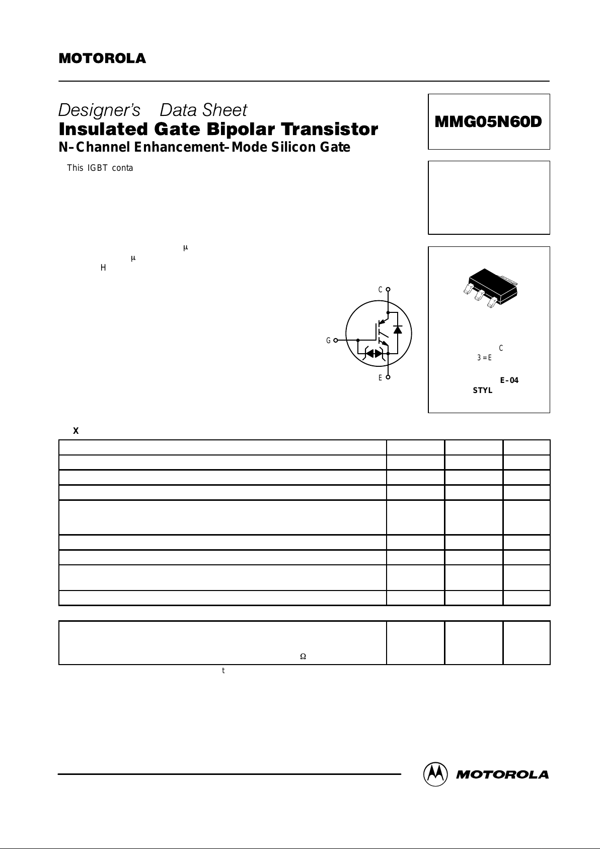
SEMICONDUCTOR TECHNICAL DATA
IGBT
0.5 A @ 25°C
600 V
CASE 318E–04
STYLE 13
TO–261A
1
2
3
4
1 = G
2 = 4 = C
3 = E
C
E
G
Motorola, Inc. 1998
Page 2
MMG05N60D
2
Motorola IGBT Device Data
ELECTRICAL CHARACTERISTICS
(T
J
= 25°C unless otherwise noted)
Characteristic
Symbol Min Typ Max Unit
OFF CHARACTERISTICS
Collector–to–Emitter Breakdown Voltage
(VGE = 0 Vdc, IC = 250 µAdc)
T emperature Coef ficient (Positive)
V
(BR)CES
600
—
680
0.7
—
—
Vdc
V/°C
Zero Gate Voltage Collector Current
(VCE = 600 Vdc, VGE = 0 Vdc, TC = 25°C)
(VCE = 600 Vdc, VGE = 0 Vdc, TC = 125°C)
I
CES
I
CES
—
—
0.1
5.0
5.0
50
µAdc
Gate–Body Leakage Current (VGE = ±15 Vdc, VCE = 0 Vdc) I
GES
— 10 100
m
Adc
ON CHARACTERISTICS
Collector–to–Emitter On–State Voltage
(VGE = 15 Vdc, IC = 0.3 Adc, TC = 25°C)
(VGE = 15 Vdc, IC = 0.3 Adc, TC = 125°C)
V
CE(on)
—
—
1.6
1.5
2.0
—
Vdc
Gate Threshold Voltage
(VCE = VGE, IC = 250 mAdc)
Threshold Temperature Coefficient (Negative)
V
GE(th)
3.5
—
—
6.0
6.0
—
Vdc
mV/°C
Forward Transconductance (VCE = 10 Vdc, IC = 0.5 Adc) g
fe
0.3 0.42 — Mhos
DYNAMIC CHARACTERISTICS
Input Capacitance
C
ies
— 75 100 pF
Output Capacitance
(VCE = 20 Vdc, VGE = 0 Vdc,
f = 1.0 MHz
)
C
oes
— 11 20
Transfer Capacitance
f = 1.0 MHz)
C
res
— 1.6 5.0
DIODE CHARACTERISTICS
Diode Forward Voltage Drop
(IEC = 0.3 Adc, TC = 25°C)
(IEC = 0.3 Adc, TC = 125°C)
(IEC = 0.1 Adc, TC = 25°C)
(IEC = 0.1 Adc, TC = 125°C)
V
FEC
—
—
—
—
5.0
5.2
2.3
2.3
6.0
—
3.0
—
Vdc
Reverse Recovery Time @ TC = 25°C
IF = 0.4 Adc, VR = 300 Vdc, dIF/dt = 10 A/ms
t
rr
— 150 —
ns
Reverse Recovery Stored Charge
IF = 0.4 Adc, VR = 300 Vdc, dIF/dt = 10 A/ms
Q
RR
— 35 —
m
C
SWITCHING CHARACTERISTICS (1)
Turn–Off Delay Time
(VCC = 300 Vdc, IC = 0.4 Adc,
t
d(off)
— 28 — ns
Fall Time
VGE = 15 Vdc, L = 3.0 mH, RG = 25 Ω,
T
= 25°C, dV/dt = 1000 V/ms
)
t
f
— 150 —
Turn–Off Switching Loss
T
C
=
25 C, dV/dt = 1000 V/ms)
Energy losses include “tail”
E
off
— 3.25 4.25
m
J
Turn–Off Delay Time
(VCC = 300 Vdc, IC = 0.4 Adc,
t
d(off)
— 21 — ns
Fall Time
VGE = 15 Vdc, L = 3.0 mH, RG = 25 Ω,
T
= 125°C, dV/dt = 1000 V/ms
)
t
f
— 280 —
Turn–Off Switching Loss
T
C
=
125 C, dV/dt = 1000 V/ms)
Energy losses include “tail”
E
off
— 8.0 10
m
J
Gate Charge (VCC = 300 Vdc, IC = 0.3 Adc,
VGE = 15 Vdc)
Q
T
— 6.4 — nC
(1) Pulse Test: Pulse Width ≤ 300 µs, Duty Cycle ≤ 2%.
Page 3

MMG05N60D
3
Motorola IGBT Device Data
Figure 1. Saturation Characteristics Figure 2. Saturation Characteristics
Figure 3. Saturation Characteristics Figure 4. Collector–To–Emitter Saturation
Voltage versus Case Temperature
Figure 5. Diode Forward Voltage Figure 6. Diode Forward Voltage versus Case
Temperature
1
VCE, COLLECTOR–TO–EMITTER VOLTAGE (VOL TS)
2.5
2.0
1.5
1.0
VCE, COLLECTOR–TO–EMITTER VOLTAGE (VOL TS)
60
1.5
0.5
0
TC, CASE TEMPERATURE (
°
C)
0–25
2.0
1.8
1.7
1.6
1.5
1.4
25
0.5 1.50
IF, INSTANTANEOUS FORWARD CURRENT (AMPS)
22
12
7
2
TC, CASE TEMPERATURE (
°
C)
50 125
10
8
6
2
0
1001.0
I
C
, COLLECTOR CURRENT (AMPS)
V
CE
, COLLECTOR–TO–EMITTER VOLTAGE (VOL TS)
0.5
0
23 12345
1.0
2.0
2.5
50 75 100 125 150
, EMITTER–TO–COLLECTOR VOLTAGE (VOLTS)V
FEC
2.0
17
25 75 150
4
V
FEC
, COLLECTOR–TO–EMITTER VOLTAGE (VOL TS)
4
I
C
, COLLECTOR CURRENT (AMPS)
1
VCE, COLLECTOR–TO–EMITTER VOLTAGE (VOL TS)
2.5
2.0
1.5
1.0
I
C
, COLLECTOR CURRENT (AMPS)
0.5
0
234
1.9
TC = 25°C
VGE = 15 V
12.5 V
10 V
8.0 V
TC = 150°C
VGE = 15 V
12.5 V
10 V
8.0 V
TC = –20°C
VGE = 15 V
12.5 V
10 V
8.0 V
700 mA
VG = 15 V
500 mA
IC = 300 mA
TC = 150°C
–20°C
25°C
500 mA
300 mA
IF = 100 mA
Page 4

MMG05N60D
4
Motorola IGBT Device Data
Figure 7. Capacitance Variation Figure 8. Gate–To–Emitter Voltage versus
Total Charge
Figure 9. Total Switching Losses versus
Collector Current
Figure 10. Total Switching Losses versus
Case Temperature
Figure 11. Minimum Turn–Off
Safe Operating Area
20 250
VCE, COLLECTOR–TO–EMITTER VOLTAGE (VOL TS)
150
100
50
Qg, TOTAL GATE CHARGE (nC)
60
10
5
0
2.00
IC, COLLECTOR CURRENT (AMPS)
60
40
30
20
10
0
TC, CASE TEMPERATURE (
°
C)
5025
20
15
10
5
0
1.5
100 3000
VCE, COLLECTOR–TO–EMITTER VOLTAGE (VOL TS)
2.5
2.0
1.5
1.0
0.5
0
200
C, CAPACITANCE (pF)
V
, TOTAL SWITCHING ENERGY LOSSES ( J)
0
10515 712345
15
m
0.5 1.0 75 100 150
, COLLECTOR CURRENT (AMPS)I
C
400 600500
, GATE–T O–EMITTER VOLTAGE (VOLTS)
GE
50
E
ts
125
, TOTAL SWITCHING ENERGY LOSSES ( J)
m
E
ts
VCE = 300 V
VGE = 15 V
IC = 0.3 A
TC = 25
°
C
TC = 25°C
VGE = 0 V
C
ies
C
oes
C
res
L = 3.0 mH
VCC = 300 V
VGE = 15 V
RG = 25
W
dV/dt = 1.0 kV/ms
TC = 125°C
25°C
L = 3.0 mH
VCC = 300 V
VGE = 15 V
RG = 25
W
dV/dt = 1.0 kV/ms
IC = 0.7 A
0.3 A
TC = 125°C
VGE = 15 V
RG = 25
W
L = 3.0 mH
Page 5

MMG05N60D
5
Motorola IGBT Device Data
t, TIME (ms)
r(t), TRANSIENT THERMAL
RESISTANCE (NORMALIZED)
1.0
0.1
0.01
D = 0.5
SINGLE PULSE
1.0E–05 1.0E–04 1.0E–03 1.0E–02 1.0E–01 1.0E+00 1.0E+01
0.2
0.1
0.05
0.02
0.01
1.0E+02 1.0E+03
0.001
R
θ
JC
(t) = r(t) R
θ
JC
R
θ
JC
= 30°C/W MAX
D CURVES APPLY FOR POWER
PULSE TRAIN SHOWN
READ TIME AT t
1
T
J(pk)
– TC = P
(pk)
R
θ
JC
(t)
P
(pk)
t
1
t
2
DUTY CYCLE, D = t1/t
2
Figure 12. Typical Thermal Response
inches
1.5
0.059
6.2
0.244
mm
1.5
0.059
1.5
0.059
2.0
0.079
2.3
0.091
4.6
0.181
2.0
0.079
3.8
0.15
Page 6

MMG05N60D
6
Motorola IGBT Device Data
P ACKAGE DIMENSIONS
CASE 318E–04
TO–261A
ISSUE H
H
S
F
A
B
D
G
L
4
123
0.08 (0003)
C
M
K
J
DIMAMIN MAX MIN MAX
MILLIMETERS
0.249 0.263 6.30 6.70
INCHES
B 0.130 0.145 3.30 3.70
C 0.060 0.068 1.50 1.75
D 0.024 0.035 0.60 0.89
F 0.115 0.126 2.90 3.20
G 0.087 0.094 2.20 2.40
H 0.0008 0.0040 0.020 0.100
J 0.009 0.014 0.24 0.35
K 0.060 0.078 1.50 2.00
L 0.033 0.041 0.85 1.05
M 0 10 0 10
S 0.264 0.287 6.70 7.30
NOTES:
1. DIMENSIONING AND TOLERANCING PER ANSI
Y14.5M, 1982.
2. CONTROLLING DIMENSION: INCH.
____
STYLE 13:
PIN 1. GATE
2. COLLECTOR
3. EMITTER
4. COLLECTOR
Motorola reserves the right to make changes without further notice to any products herein. Motorola makes no warranty , representation or guarantee regarding
the suitability of its products for any particular purpose, nor does Motorola assume any liability arising out of the application or use of any product or circuit, and
specifically disclaims any and all liability, including without limitation consequential or incidental damages. “T ypical” parameters which may be provided in Motorola
data sheets and/or specifications can and do vary in different applications and actual performance may vary over time. All operating parameters, including “Typicals”
must be validated for each customer application by customer’s technical experts. Motorola does not convey any license under its patent rights nor the rights of
others. Motorola products are not designed, intended, or authorized for use as components in systems intended for surgical implant into the body, or other
applications intended to support or sustain life, or for any other application in which the failure of the Motorola product could create a situation where personal injury
or death may occur. Should Buyer purchase or use Motorola products for any such unintended or unauthorized application, Buyer shall indemnify and hold Motorola
and its officers, employees, subsidiaries, affiliates, and distributors harmless against all claims, costs, damages, and expenses, and reasonable attorney fees
arising out of, directly or indirectly, any claim of personal injury or death associated with such unintended or unauthorized use, even if such claim alleges that
Motorola was negligent regarding the design or manufacture of the part. Motorola and are registered trademarks of Motorola, Inc. Motorola, Inc. is an Equal
Opportunity/Affirmative Action Employer.
Mfax is a trademark of Motorola, Inc.
How to reach us:
USA/EUROPE /Locations Not Listed: Motorola Literature Distribution; JAPAN: Nippon Motorola Ltd.: SPD, Strategic Planning Office, 141,
P.O. Box 5405, Denver, Colorado 80217. 1–303–675–2140 or 1–800–441–2447 4–32–1 Nishi–Gotanda, Shagawa–ku, Tokyo, Japan. 03–5487–8488
Customer Focus Center: 1–800–521–6274
Mfax: RMFAX0@email.sps.mot.com – TOUCHTONE 1–602–244–6609 ASIA/PACIFIC: Motorola Semiconductors H.K. Ltd.; 8B Tai Ping Industrial Park,
Moto rola Fax Back System – US & Canada ONLY 1–800–774–1848 51 Ting Kok Road, Tai Po, N.T., Hong Kong. 852–26629298
– http://sps.motorola.com/mfax/
HOME PAGE: http://motorola.com/sps/
MMG05N60D/D
◊
 Loading...