

Page 1
1
Motorola TMOS Power MOSFET Transistor Device Data
N–Channel Enhancement Mode
Silicon Gate TMOS E–FET
t
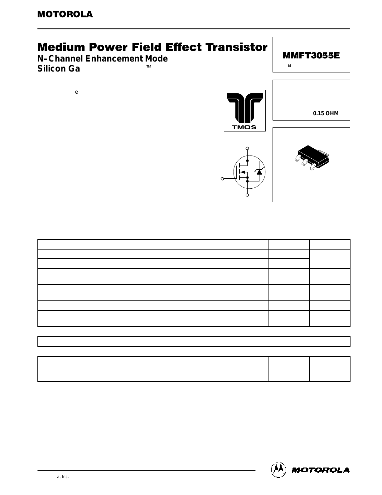
SOT–223 for Surface Mount
This advanced E–FET is a TMOS Medium Power MOSFET
designed to withstand high energy in the avalanche and commutation m odes. T his n ew e nergy efficient d evice a lso offers a
drain–to–source diode with a fast recovery time. Designed for low
voltage, high speed switching applications in power supplies,
dc–dc converters and PWM motor controls, these devices are
particularly well suited for bridge circuits where diode speed and
commutating safe operating areas are critical and offer additional
safety margin against unexpected voltage transients. The device is
housed in the SOT–223 package which is designed for medium
power surface mount applications.
• Silicon Gate for Fast Switching Speeds
• Low R
DS(on)
— 0.15 Ω max
• The SOT–223 Package can be Soldered Using Wave or Re-
flow. The Formed Leads Absorb Thermal Stress During Soldering, Eliminating the Possibility of Damage to the Die
• Available in 12 mm Tape and Reel
Use MMFT3055ET1 to order the 7 inch/1000 unit reel.
Use MMFT3055ET3 to order the 13 inch/4000 unit reel.
MAXIMUM RATINGS
(TA = 25°C unless otherwise noted)
Rating
Symbol Value Unit
Drain–to–Source Voltage V
DS
60
Gate–to–Source Voltage — Continuous V
GS
±20
Vdc
Drain Current — Continuous
Drain Current — Pulsed
I
D
I
DM
1.7
6.8
Adc
Total Power Dissipation @ TA = 25°C
Derate above 25°C
P
D
(1)
0.8
6.4
Watts
mW/°C
Operating and Storage Temperature Range TJ, T
stg
–65 to 150 °C
Single Pulse Drain–to–Source Avalanche Energy — Starting TJ = 25°C
(VDD = 60 V, VGS = 10 V, Peak IL= 1.7 A, L = 0.2 mH, RG = 25 Ω)
E
AS
168 mJ
DEVICE MARKING
3055
THERMAL CHARACTERISTICS
Thermal Resistance — Junction–to–Ambient (surface mounted) R
θJA
156 °C/W
Maximum Temperature for Soldering Purposes,
Time in Solder Bath
T
L
260
10
°C
Sec
(1) Power rating when mounted on FR–4 glass epoxy printed circuit board using recommended footprint.
TMOS is a registered trademark of Motorola, Inc.
E–FET is a trademark of Motorola, Inc.
Thermal Clad is a trademark of the Bergquist Company
Preferred devices are Motorola recommended choices for future use and best overall value.
REV 3
Order this document
by MMFT3055E/D
SEMICONDUCTOR TECHNICAL DATA
Motorola, Inc. 1995
MEDIUM POWER
TMOS FET
1.7 AMP
60 VOLTS
R
DS(on)
= 0.15 OHM
Motorola Preferred Device
CASE 318E–04, STYLE 3
TO–261AA
D
S
G
2,4
3
1
1
2
3
4
Page 2
MMFT3055E
2
Motorola TMOS Power MOSFET Transistor Device Data
ELECTRICAL CHARACTERISTICS
(TA = 25°C unless otherwise noted)
Characteristic
Symbol Min Typ Max Unit
OFF CHARACTERISTICS
Drain–to–Source Breakdown Voltage, (VGS = 0, ID = 250 µA) V
(BR)DSS
60 — — Vdc
Zero Gate Voltage Drain Current, (VDS = 60 V, VGS = 0) I
DSS
— — 10 µAdc
Gate–Body Leakage Current, (VGS = 20 V, VDS = 0) I
GSS
— — 100 nAdc
ON CHARACTERISTICS
Gate Threshold Voltage, (VDS = VGS, ID = 1 mA) V
GS(th)
2 — 4.5 Vdc
Static Drain–to–Source On–Resistance, (VGS = 10 V, ID = 0.85 A) R
DS(on)
— — 0.15 Ohms
Drain–to–Source On–Voltage, (VGS = 10 V, ID = 1.7 A) V
DS(on)
— — 0.34 Vdc
Forward Transconductance, (VDS = 15 V, ID = 0.85 A) g
FS
— 2.2 — mhos
DYNAMIC CHARACTERISTICS
Input Capacitance
C
iss
— 430 —
Output Capacitance
(VDS = 20 V,
VGS = 0,
C
oss
— 225 —
Reverse Transfer Capacitance
f = 1 MHz)
C
rss
— 40 —
SWITCHING CHARACTERISTICS
Turn–On Delay Time
t
d(on)
— 15 —
Rise Time
t
r
— 22 —
Turn–Off Delay Time
VGS = 10 V, RG = 50 ohms,
RGS = 25 ohms)
t
d(off)
— 31 —
ns
Fall Time
GS
= 25 ohms)
t
f
— 49 —
Total Gate Charge
Q
g
— 12.5 —
Gate–Source Charge
(VDS = 48 V, ID = 1.7 A,
VGS = 10 Vdc)
Q
gs
— 2 —
Gate–Drain Charge
See Figures 15 and 16
Q
gd
— 4.5 —
SOURCE DRAIN DIODE CHARACTERISTICS
(1)
Forward On–Voltage IS = 1.7 A, VGS = 0 V
SD
— 0.8 — Vdc
Forward Turn–On Time
t
on
Limited by stray inductance
Reverse Recovery Time
dlS/dt = 400 A/µs,
VR = 30 V
t
rr
— 50 —
ns
(1) Pulse Test: Pulse Width ≤ 300 µs, Duty Cycle ≤ 2%
(VDD = 25 V, ID = 0.85 A
IS = 1.7 A, VGS = 0,
pF
nC
Page 3
MMFT3055E
3
Motorola TMOS Power MOSFET Transistor Device Data
R
DS(on)
, DRAIN–TO–SOURCE RESISTANCE (OHMS)
10
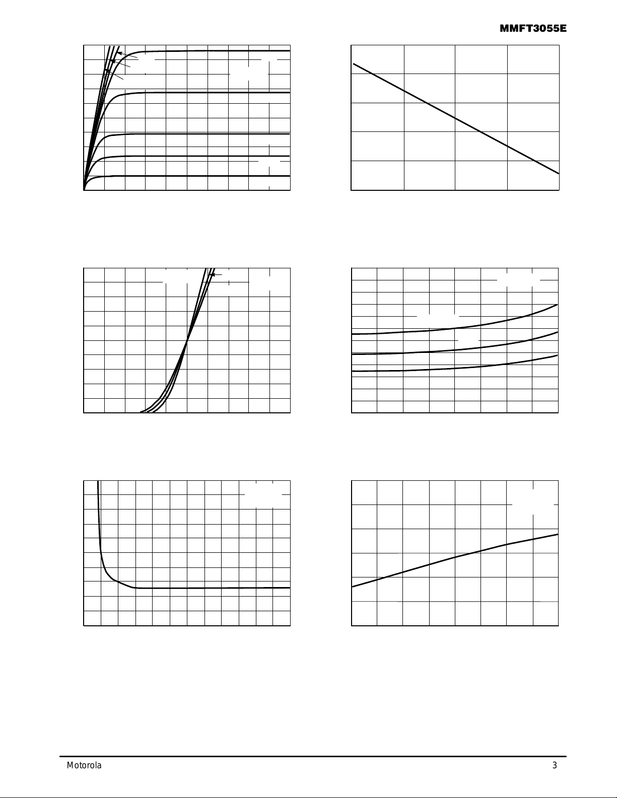
Figure 1. On Region Characteristics
VDS, DRAIN–TO–SOURCE VOLTAGE (VOLTS)
6 V
Figure 2. Gate–Threshold Voltage Variation
With Temperature
TJ, JUNCTION TEMP (°C)
Figure 3. Transfer Characteristics
VGS, GATE–TO–SOURCE VOLTAGE (VOLTS)
Figure 4. On–Resistance versus Drain Current
ID, DRAIN CURRENT (AMPS)
Figure 5. On–Resistance versus
Gate–to–Source Voltage
VGS, GATE–TO–SOURCE VOLTAGE (VOLTS)
Figure 6. On–Resistance versus Junction
Temperature
TJ, JUNCTION TEMPERATURE (°C)
VDS = V
GS
ID = 1 mA
I
D
, DRAIN CURRENT (AMPS)
8
6
4
2
0
1086420
V
GS(TH)
, GATE THRESHOLD VOLTAGE
(NORMALIZED)
1.1
–50
1
0.9
0.8
0.7
0 50 100 150
10
I
D
, DRAIN CURRENT (AMPS)
8
6
2
0
1086420
0.3
0
0.2
0.15
0.1
0
2 4 6 8
0.25
VGS = 10 V
25°C
–55
°
C
0.5
0.4
0.3
0.1
0
211512963
0.3
–50
0.1
0
0 50 100 150
0.2
0.2
18
4
0.05
5 V
TJ = 25°C
ID = 1.7 A
VGS = 10 V
ID = 1.7 A
VGS = 20 V
4.5 V
4 V
10 V
8 V
1.2
TJ = 25°C
7 V
100°C
VDS = 10 V
25°C
TJ = –55°C
TJ = 100°C
, DRAIN–TO–SOURCE RESISTANCE (OHMS)R
DS(on)
R
, DRAIN–TO–SOURCE RESISTANCE (OHMS)
DS(on)
Page 4

MMFT3055E
4
Motorola TMOS Power MOSFET Transistor Device Data
FORWARD BIASED SAFE OPERATING AREA
The FBSOA curves define the maximum drain–to–source
voltage and drain current that a device can safely handle
when it is forward biased, or when it is on, or being turned on.
Because these curves include the limitations of simultaneous
high voltage and high current, up to the rating of the device,
they are especially useful to designers of linear systems. The
curves are based on an ambient temperature of 25
°C and a
maximum junction temperature of 150
°C. Limitations for re-
petitive pulses at various ambient temperatures can be determined by using the thermal response curves. Motorola
Application Note, AN569, “Transient Thermal Resistance–
General Data and Its Use” provides detailed instructions.
SWITCHING SAFE OPERATING AREA
The switching safe operating area (SOA) is the boundary
that the load line may traverse without incurring damage to
the MOSFET. The fundamental limits are the peak current,
IDM and the breakdown voltage, BV
DSS
. The switching SOA
is applicable for both turn–on and turn–off of the devices for
switching times less than one microsecond.
Figure 7. Maximum Rated Forward Biased
Safe Operating Area
VGS = 20 V
SINGLE PULSE
TA = 25
°
C
DC
10
I
D
, DRAIN CURRENT (AMPS)
0.1
1
0.1
0.01
1 10 100
VDS, DRAIN–TO–SOURCE VOLTAGE (VOLTS)
20 ms
100 ms
1 s
500 ms
R
DS(on)
LIMIT
THERMAL LIMIT
PACKAGE LIMIT
1.0
0.1
0.001
r(t), EFFECTIVE THERMAL RESISTANCE
t, TIME (s)
0.1
0.01
0.2
0.02
0.01
D = 0.5
SINGLE PULSE
(NORMALIZED)
0.05
R
θ
JA
(t) = r(t) R
θ
JA
R
θ
JA
= 156
°
C/W MAX
D CURVES APPLY FOR POWER
PULSE TRAIN SHOWN
READ TIME AT t
1
T
J(pk)
– TA = P
(pk)
R
θ
JA
(t)
P
(pk)
t
1
t
2
DUTY CYCLE, D = t1/t
2
Figure 8. Thermal Response
1.0E–05 1.0E–04 1.0E–03 1.0E–02 1.0E–01 1.0E+00 1.0E+01
COMMUTATING SAFE OPERATING AREA (CSOA)
The Commutating Safe Operating Area (CSOA) of Figure 10 defines the limits of safe operation for commutated source–drain
current versus re–applied drain voltage when the source–drain diode has undergone forward bias. The curve shows the limitations of IFM and peak VDS for a given rate of change of source current. It is applicable when waveforms similar to those of Figure
9 are present. Full or half–bridge PWM DC motor controllers are common applications requiring CSOA data.
Device stresses increase with increasing rate of change of source current so dIS/dt is specified with a maximum value. Higher
values of dIS/dt require an appropriate derating of IFM, peak VDS or both. Ultimately dIS/dt is limited primarily by device, package,
and circuit impedances. Maximum device stress occurs during trr as the diode goes from conduction to reverse blocking.
V
DS(pk)
is the peak drain–to–source voltage that the device must sustain during commutation; IFM is the maximum forward
source–drain diode current just prior to the onset of commutation.
VR is specified at 80% rated BV
DSS
to ensure that the CSOA stress is maximized as IS decays from IRM to zero.
RGS should be minimized during commutation. TJ has only a second order effect on CSOA.
Stray inductances in Motorola’s test circuit are assumed to be practical minimums. dVDS/dt in excess of 10 V/ns was at-
tained with dIS/dt of 400 A/µs.
Page 5

MMFT3055E
5
Motorola TMOS Power MOSFET Transistor Device Data
R
G
t
V
DS
L
I
L
V
DD
Figure 9. Commutating Waveforms
t
P
BV
DSS
V
DD
I
L(t)
t, (TIME)
Figure 10. Commutating Safe Operating
Area (CSOA)
15 V
V
GS
0
90%
I
FM
dlS/dt
I
S
10%
t
rr
t
frr
0.25 I
RM
I
RM
t
on
V
DS
V
f
V
dsL
V
R
V
DS(pk)
MAX. CSOA
STRESS AREA
Figure 11. Commutating Safe Operating Area
Test Circuit
+
–
+
–
Figure 12. Unclamped Inductive Switching
Test Circuit
V
R
V
GS
I
FM
20 V
R
GS
DUT
I
S
L
i
VR = 80% OF RATED V
DSS
V
dsL
= Vf + Li
⋅
dlS/dt
Figure 13. Unclamped Inductive Switching
Waveforms
VDS, DRAIN–TO–SOURCE VOLTAGE (VOLTS)
I
S
, SOURCE CURRENT (AMPS)
10
0
8
6
4
2
0
20 40 60 80 10010 30 50 70 90
9
7
5
3
1
dIS/dt ≤ 400 A/µs
V
DS
Page 6

MMFT3055E
6
Motorola TMOS Power MOSFET Transistor Device Data
Figure 14. Capacitance Variation With Voltage
SAME
DEVICE TYPE
AS DUT
V
in
+18 V V
DD
10 V
100 k
0.1
µ
F
FERRITE
BEAD
DUT
100
2N3904
2N3904
47 k
15 V
100 k
Vin = 15 Vpk; PULSE WIDTH
≤
100 µs, DUTY CYCLE ≤ 10%.
1 mA
47 k
Figure 15. Gate Charge versus
Gate–To–Source Voltage
GATE–TO–SOURCE OR DRAIN–TO–SOURCE VOLTAGE (VOLTS)
C, CAPACITANCE (pF)
C
rss
C
iss
C
oss
1400
20
1200
1000
800
600
400
200
0
15 10 5 0 5 10 15 20
Figure 16. Gate Charge Test Circuit
Qg, TOTAL GATE CHARGE (nC)
16
0
14
12
10
0
2 4 6 20
V
GS
, GATE–TO–SOURCE VOLTAGE (VOLTS)
VDS = 36 V
8
6
4
2
8 10 12 14 16 18
48 V
V
GS
V
DS
TJ = 25°C
f = 1 MHz
TJ = 25°C
ID = 1.7 A
VGS = 10 V
Page 7

MMFT3055E
7
Motorola TMOS Power MOSFET Transistor Device Data
INFORMATION FOR USING THE SOT–223 SURFACE MOUNT PACKAGE
MINIMUM RECOMMENDED FOOTPRINT FOR SURFACE MOUNTED APPLICATIONS
Surface mount board layout is a critical portion of the total
design. The footprint for the semiconductor packages must be
the correct size to insure proper solder connection interface
between the board and the package. With the correct pad
geometry, the packages will self align when subjected to a
solder reflow process.
0.079
2.0
0.15
3.8
0.248
6.3
0.079
2.0
0.059
1.5
0.059
1.5
0.059
1.5
0.091
2.3
0.091
2.3
mm
inches
SOT–223 POWER DISSIPATION
The power dissipation of the SOT–223 is a function of the
drain pad size. This can vary from the minimum pad size for
soldering to a pad size given for maximum power dissipation.
Power dissipation for a surface mount device is determined by
T
J(max)
, the maximum rated junction temperature of the die,
R
θJA
, the thermal resistance from the device junction to
ambient, and the operating temperature, TA. Using the values
provided on the data sheet for the SOT–223 package, PD can
be calculated as follows:
PD =
T
J(max)
– T
A
R
θJA
The values for the equation are found in the maximum
ratings table on the data sheet. Substituting these values into
the equation for an ambient temperature TA of 25°C, one can
calculate the power dissipation of the device which in this case
is 800 milliwatts.
PD =
150°C – 25°C
156°C/W
= 800 milliwatts
The 156°C/W for the SOT–223 package assumes the use
of the recommended footprint on a glass epoxy printed circuit
board to achieve a power dissipation of 800 milliwatts. There
are other alternatives to achieving higher power dissipation
from the SOT–223 package. One is to increase the area of the
drain pad. By increasing the area of the drain pad, the power
dissipation can be increased. Although one can almost double
the power dissipation with this method, one will be giving up
area on the printed circuit board which can defeat the purpose
of using surface mount technology. A graph of R
θJA
versus
drain pad area is shown in Figure 17.
0.8 Watts
1.25 Watts* 1.5 Watts
R , Thermal Resistance, Junction
to Ambient ( C/W)
θ
JA
°
A, Area (square inches)
0.0 0.2 0.4 0.6 0.8 1.0
160
140
120
100
80
Figure 17. Thermal Resistance versus Drain Pad
Area for the SOT–223 Package (Typical)
Board Material = 0.0625
″
G–10/FR–4, 2 oz Copper
TA = 25°C
*Mounted on the DPAK footprint
Another alternative would be to use a ceramic substrate or
an aluminum core board such as Thermal Clad. Using a
board material such as Thermal Clad, an aluminum core
board, the power dissipation can be doubled using the same
footprint.
SOT–223
Page 8

MMFT3055E
8
Motorola TMOS Power MOSFET Transistor Device Data
SOLDER STENCIL GUIDELINES
Prior to placing surface mount components onto a printed
circuit board, solder paste must be applied to the pads. A
solder stencil is required to screen the optimum amount of
solder paste onto the footprint. The stencil is made of brass or
stainless steel with a typical thickness of 0.008 inches. The
stencil opening size for the SOT–223 package should be the
same as the pad size on the printed circuit board, i.e., a 1:1
registration.
SOLDERING PRECAUTIONS
The melting temperature of solder is higher than the rated
temperature of the device. When the entire device is heated
to a high temperature, failure to complete soldering within a
short time could result in device failure. Therefore, the
following items should always be observed in order to
minimize the thermal stress to which the devices are
subjected.
• Always preheat the device.
• The delta temperature between the preheat and soldering
should be 100°C or less.*
• When preheating and soldering, the temperature of the
leads and the case must not exceed the maximum
temperature ratings as shown on the data sheet. When
using infrared heating with the reflow soldering method,
the difference shall be a maximum of 10°C.
• The soldering temperature and time shall not exceed
260°C for more than 10 seconds.
• When shifting from preheating to soldering, the maximum
temperature gradient shall be 5°C or less.
• After soldering has been completed, the device should be
allowed to cool naturally for at least three minutes.
Gradual cooling should be used as the use of forced
cooling will increase the temperature gradient and result
in latent failure due to mechanical stress.
• Mechanical stress or shock should not be applied during
cooling
* Soldering a device without preheating can cause excessive
thermal shock and stress which can result in damage to the
device.
TYPICAL SOLDER HEATING PROFILE
For any given circuit board, there will be a group of control
settings that will give the desired heat pattern. The operator
must set temperatures for several heating zones, and a figure
for belt speed. T aken together , these control settings make up
a heating “profile” for that particular circuit board. On
machines controlled by a computer, the computer remembers
these profiles from one operating session to the next. Figure
18 shows a typical heating profile for use when soldering a
surface mount device to a printed circuit board. This profile will
vary among soldering systems but it is a good starting point.
Factors that can affect the profile include the type of soldering
system in use, density and types of components on the board,
type of solder used, and the type of board or substrate material
being used. This profile shows temperature versus time. The
line on the graph shows the actual temperature that might be
experienced on the surface of a test board at or near a central
solder joint. The two profiles are based on a high density and
a low density board. The Vitronics SMD310 convection/infrared reflow soldering system was used to generate this
profile. The type of solder used was 62/36/2 Tin Lead Silver
with a melting point between 177–189°C. When this type of
furnace is used for solder reflow work, the circuit boards and
solder joints tend to heat first. The components on the board
are then heated by conduction. The circuit board, because it
has a large surface area, absorbs the thermal energy more
efficiently, then distributes this energy to the components.
Because of this effect, the main body of a component may be
up to 30 degrees cooler than the adjacent solder joints.
STEP 1
PREHEAT
ZONE 1
“RAMP”
STEP 2
VENT
“SOAK”
STEP 3
HEATING
ZONES 2 & 5
“RAMP”
STEP 4
HEATING
ZONES 3 & 6
“SOAK”
STEP 5
HEATING
ZONES 4 & 7
“SPIKE”
STEP 6
VENT
STEP 7
COOLING
200°C
150
°
C
100
°
C
50
°
C
TIME (3 TO 7 MINUTES TOTAL)
T
MAX
SOLDER IS LIQUID FOR
40 TO 80 SECONDS
(DEPENDING ON
MASS OF ASSEMBLY)
205
°
TO 219°C
PEAK AT
SOLDER JOINT
DESIRED CURVE FOR LOW
MASS ASSEMBLIES
100°C
150°C
160
°
C
170°C
140
°
C
Figure 18. Typical Solder Heating Profile
DESIRED CURVE FOR HIGH
MASS ASSEMBLIES
Page 9

MMFT3055E
9
Motorola TMOS Power MOSFET Transistor Device Data
PACKAGE DIMENSIONS
CASE 318E–04
TO–261AA
SOT–223
ISSUE H
STYLE 3:
PIN 1. GATE
2. DRAIN
3. SOURCE
4. DRAIN
H
S
F
A
B
D
G
L
4
1 2 3
0.08 (0003)
C
M
K
J
DIMAMIN MAX MIN MAX
MILLIMETERS
0.249 0.263 6.30 6.70
INCHES
B 0.130 0.145 3.30 3.70
C 0.060 0.068 1.50 1.75
D 0.024 0.035 0.60 0.89
F 0.115 0.126 2.90 3.20
G 0.087 0.094 2.20 2.40
H 0.0008 0.0040 0.020 0.100
J 0.009 0.014 0.24 0.35
K 0.060 0.078 1.50 2.00
L 0.033 0.041 0.85 1.05
M 0 10 0 10
S 0.264 0.287 6.70 7.30
NOTES:
1. DIMENSIONING AND TOLERANCING PER ANSI
Y14.5M, 1982.
2. CONTROLLING DIMENSION: INCH.
_ _ _ _
Page 10

MMFT3055E
10
Motorola TMOS Power MOSFET Transistor Device Data
Motorola reserves the right to make changes without further notice to any products herein. Motorola makes no warranty , representation or guarantee regarding
the suitability of its products for any particular purpose, nor does Motorola assume any liability arising out of the application or use of any product or circuit,
and specifically disclaims any and all liability, including without limitation consequential or incidental damages. “T ypical” parameters can and do vary in different
applications. All operating parameters, including “T ypicals” must be validated for each customer application by customer’s technical experts. Motorola does
not convey any license under its patent rights nor the rights of others. Motorola products are not designed, intended, or authorized for use as components in
systems intended for surgical implant into the body, or other applications intended to support or sustain life, or for any other application in which the failure of
the Motorola product could create a situation where personal injury or death may occur. Should Buyer purchase or use Motorola products for any such
unintended or unauthorized application, Buyer shall indemnify and hold Motorola and its officers, employees, subsidiaries, affiliates, and distributors harmless
against all claims, costs, damages, and expenses, and reasonable attorney fees arising out of, directly or indirectly, any claim of personal injury or death
associated with such unintended or unauthorized use, even if such claim alleges that Motorola was negligent regarding the design or manufacture of the part.
Motorola and are registered trademarks of Motorola, Inc. Motorola, Inc. is an Equal Opportunity/Affirmative Action Employer.
Literature Distribution Centers:
USA: Motorola Literature Distribution; P.O. Box 20912; Phoenix, Arizona 85036.
EUROPE: Motorola Ltd.; European Literature Centre; 88 T anners Drive, Blakelands, Milton Keynes, MK14 5BP, England.
JAPAN: Nippon Motorola Ltd.; 4–32–1, Nishi–Gotanda, Shinagawa–ku, Tokyo 141, Japan.
ASIA PACIFIC: Motorola Semiconductors H.K. Ltd.; Silicon Harbour Center, No. 2 Dai King Street, Tai Po Industrial Estate, Tai Po, N.T., Hong Kong.
MMFT3055E/D
*MMFT3055E/D*
◊
 Loading...