

Page 1
SEMICONDUCTOR TECHNICAL DATA
Order this document
by MMFT2N25E/D
N–Channel Enhancement–Mode Silicon Gate
This advanced high voltage TMOS E–FET is designed to
withstand high energy in the avalanche mode and switch efficiently .
This new high energy device also offers a drain–to–source diode
with fast recovery time. Designed for high voltage, high speed
switching applications such as power supplies, PWM motor
controls and other inductive loads, the avalanche energy capability
is specified to eliminate the guesswork in designs where inductive
loads are switched and offer additional safety margin against
unexpected voltage transients.
• Avalanche Energy Capability Specified at Elevated
Temperature
• Internal Source–to–Drain Diode Designed to Replace External
Zener Transient Suppressor – Absorbs High Energy in the
1
G
Avalanche Mode
• Source–to–Drain Diode Recovery Time Comparable to
Discrete Fast Recovery Diode
MAXIMUM RATINGS
Drain–to–Source Voltage V
Drain–to–Gate Voltage, RGS = 1.0 m
Gate–to–Source Voltage — Continuous V
Gate–to–Source Voltage — Single Pulse (tp ≤ 50 mS)
Drain Current — Continuous @ TC = 25°C
Drain Current — Continuous @ TC = 100°C
Drain Current — Single Pulse (tp ≤ 10 mS)
Total Power Dissipation @ TC = 25°C
Derate above 25°C
Total PD @ TA = 25°C mounted on 1″ Sq. Drain Pad on FR–4 Bd. Material
Total PD @ TA = 25°C mounted on 0.7″ Sq. Drain Pad on FR–4 Bd. Material
Total PD @ TA = 25°C mounted on min. Drain Pad on FR–4 Bd. Material
Operating and Storage Temperature Range TJ, T
(TC = 25°C unless otherwise noted)
Rating
W
UNCLAMPED DRAIN–TO–SOURCE AVALANCHE CHARACTERISTICS (TJ < 150°C)
Single Pulse Drain–to–Source Avalanche Energy — Starting TJ = 25°C
(VDD = 80 V, VGS = 10 V, Peak IL= 4.0 Apk, L = 3.0 mH, RG = 25 Ω)
2,4
D
S
3
Symbol Value Unit
V
V
I
E
DSS
DGR
GS
GSM
I
D
I
D
DM
P
D
stg
AS
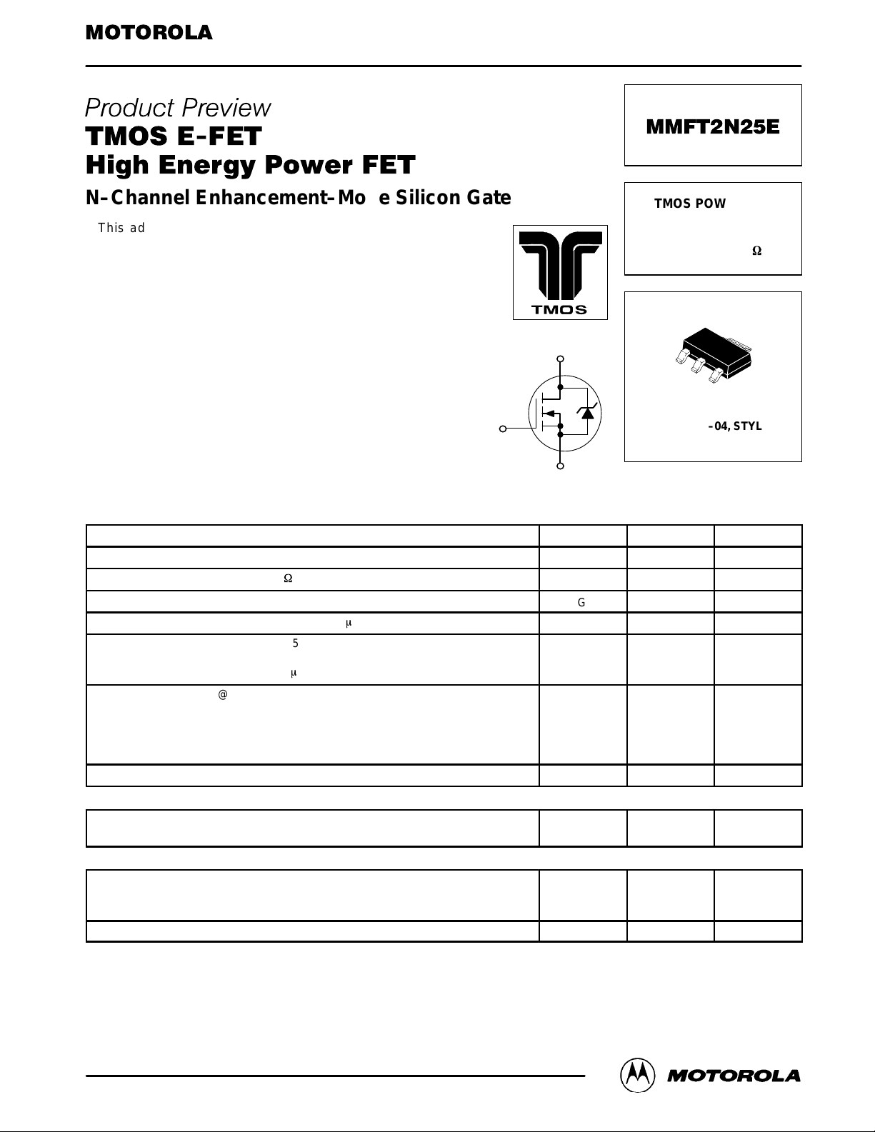
TMOS POWER FET
2.0 AMPERES
250 VOL TS
R
1
CASE 318E–04, STYLE 3
250 Vdc
250 Vdc
±20 Vdc
±40 Vdc
2.0
0.6
7.0
0.77
6.2
1.0
1.2
0.8
–55 to 150 °C
26
DS(on)
2
3
TO–261AA
= 3.5
mW/°C
W
4
Adc
Apk
Watts
Watts
mJ
THERMAL CHARACTERISTICS
— Junction–to–Ambient on 1″ Sq. Drain Pad on FR–4 Bd. Material
— Junction–to–Ambient on 0.7″ Sq. Drain Pad on FR–4 Bd. Material
— Junction–to–Ambient on min. Drain Pad on FR–4 Bd. Material
Maximum Lead Temperature for Soldering Purposes, 1/8″ from case for 10 seconds T
This document contains information on a product under development. Motorola reserves the right to change or discontinue this product without notice.
TMOS is a registered trademark of Motorola, Inc.
E–FET is a trademark of Motorola, Inc.
Motorola TMOS Power MOSFET Transistor Device Data
Motorola, Inc. 1997
R
θJA
L
90
103
162
260 °C
°C/W
1
Page 2

MMFT2N25E
(V
DS
(V
125 V
D
,
V
V)
I
2.0 A
GS
)
(
S
,
ELECTRICAL CHARACTERISTICS
Characteristic Symbol Min Typ Max Unit
OFF CHARACTERISTICS
Drain–to–Source Breakdown Voltage
(VGS = 0, ID = 0.25 mA)
T emperature Coef ficient (Positive)
Zero Gate Voltage Drain Current
(VDS = 250 V, VGS = 0)
(VDS = 250 V, VGS = 0, TJ = 125°C)
Gate–Body Leakage Current
(VGS = ±20 V , VDS = 0)
ON CHARACTERISTICS
Gate Threshold Voltage
(VDS = VGS, ID = 0.25 mA)
Threshold Temperature Coefficient (Negative)
Static Drain–to–Source On–Resistance
(VGS = 10 V, ID = 1.0 Adc)
Drain–to–Source On–Voltage
(VGS = 10 V, ID = 2.0 A)
(VGS = 10 V, ID = 1.0 A, TJ = 125°C)
Forward Transconductance
(VDS = 8.0 V, ID = 2.0 Adc)
DYNAMIC CHARACTERISTICS
Input Capacitance
Output Capacitance
Transfer Capacitance
SWITCHING CHARACTERISTICS
Turn–On Delay Time
Rise Time
Turn–Off Delay Time
Fall Time
Gate Charge
SOURCE–DRAIN DIODE CHARACTERISTICS
Forward On–Voltage
Reverse Recovery Time
Reverse Recovery Stored Charge q
(1) Pulse Test: Pulse Width ≤300 µS, Duty Cycle ≤ 2%.
(1)
(TC = 25°C unless otherwise noted)
V
= 25 V
= 25 V,
VGS = 0,
f = 1.0 MHz)
(1)
=
DS
ID = 2.0 A,
RG = 9.1 Ohms,
GS
(VDS = 200 V,
=
D
VGS = 10 V)
IS = 2.0 A, VGS = 0 V V
IS = 2.0 A, VGS = 0 V, TJ = 125°C V
(IS = 2.0 A,
dlS/dt = 100 A/µs)
,
= 10
,
BV
I
DSS
I
GSS
V
GS(th)
R
DS(on)
V
DS(on)
g
C
C
C
t
d(on)
t
d(off)
Q
Q
Q
Q
DSS
FS
iss
oss
rss
t
r
t
f
T
1
2
3
SD
SD
t
rr
t
a
t
b
rr
250
—
—
—
— — 100
2.0
—
— 2.1 3.5
—
—
0.44 1.2 —
— 137 190
— 30 40
— 7.0 10
— 9.2 20
— 6.6 10
— 13 30
— 8.5 20
— 4.7 10
— 1.3 —
— 3.2 —
— 2.3 —
— 0.94 2.0
— 0.83 —
— 104 —
— 63 —
— 41 —
— 0.365 —
—
324
—
—
2.8
5.7
—
—
—
—
10
100
4.0
—
8.40
7.35
Vdc
V/°C
µAdc
nAdc
Vdc
mV/°C
Ohms
Vdc
mhos
pF
ns
nC
Vdc
nS
m
C
2
Motorola TMOS Power MOSFET Transistor Device Data
Page 3

4.0
3.5
3.0
2.5
2.0
1.5
, DRAIN CURRENT (AMPS)
1.0
D
I
0.5
0
TJ = 25°C
9.0 V
VDS, DRAIN–TO–SOURCE VOL TAGE (VOLTS)
VGS = 10 V
105.0 15
8.0 V
7.0 V
6.0 V
5.0 V
200
4.0
3.5
3.0
2.5
2.0
1.5
, DRAIN CURRENT (AMPS)
1.0
D
I
0.5
0
VDS ≥ 10 V
–55°C
6.0 7.53.0
VGS, GATE–T O–SOURCE VOLTAGE (VOLTS)
Figure 1. On–Region Characteristics Figure 2. Transfer Characteristics
MMFT2N25E
TJ = 100°C
25°C
6.5 7.03.5 4.0 4.5 5.0 5.5
7.0
VGS = 10 V
6.0
5.0
4.0
3.0
2.0
1.0
, DRAIN–TO–SOURCE RESIST ANCE (OHMS)
0
DS(on)
R
1.0 2.0 2.0 2.5 3.0 3.5 4.0
ID, DRAIN CURRENT (AMPS)
TJ = 100°C
Figure 3. On–Resistance versus Drain Current
and T emperature
2.5
VGS = 10 V
ID = 1.0 A
2.0
1.5
1.0
0.5
6.0
TJ = 25°C
5.0
25°C
–55°C
3.0 4.00
4.0
3.0
2.0
1.0
, DRAIN–TO–SOURCE RESIST ANCE (OHMS)
0
DS(on)
R
0.5
VGS = 10 V
1.00
1.5
ID, DRAIN CURRENT (AMPS)
15 V
Figure 4. On–Resistance versus Drain Current
and Gate Voltage
100
VGS = 0 V
10
, LEAKAGE (nA)
DSS
I
TJ = 125°C
100°C
, DRAIN–TO–SOURCE RESIST ANCE (NORMALIZED)R
0
DS(on)
–25 25–50
TJ, JUNCTION TEMPERATURE (
50 75 100
°
C)
125 150
Figure 5. On–Resistance Variation versus
T emperature
Motorola TMOS Power MOSFET Transistor Device Data
1.0
500
VDS, DRAIN–TO–SOURCE VOL TAGE (VOL TS)
1000
Figure 6. Drain–to–Source Leakage Current
versus V oltage
200 250150
3
Page 4

MMFT2N25E
C, CAPACITANCE (pF)
350
300
250
200
150
100
50
0
VGS = 0 V VDS = 0 V
C
iss
C
rss
GATE–T O–SOURCE OR DRAIN–TO–SOURCE VOLTAGE (VOL TS)
C
rss
V
GS
0205.0
V
DS
10–5.0 15
Figure 7. Capacitance Variation
TJ = 25°C
C
C
iss
oss
12
QT
10
V
DS
8.0
Q2Q1
6.0
4.0
2.0
, GATE–T O–SOURCE VOLTAGE (VOLTS)
GS
V
25–10
Q3
0
QG, TOTAL GATE CHARGE (nC)
V
GS
TJ = 25°C
ID = 2.0 A
6.0 100
8.02.0 4.0
250
200
150
100
50
0
, DRAIN–TO–SOURCE VOL TAGE (VOL TS)
DS
V
Figure 8. Gate–to–Source and
Drain–to–Source V oltage versus Total Charge
100
TJ = 25°C
ID = 2.0 A
VDD = 125 V
VGS = 10 V
t
d(off)
10
t, TIME (ns)
1.0
1.0 10 0.7 0.8 0.9 1.0
t
f
t
r
RG, GATE RESISTANCE (OHMS)
t
d(on)
100
Figure 9. Resistive Switching Time V ariation
versus Gate Resistance
10
VGS = 20 V
SINGLE PULSE
TC = 25
1.0
°
C
1.0 ms
10 ms
100 ms
2.0
1.5
1.0
0.5
, SOURCE CURRENT (AMPS)
S
I
0
60
50
40
TJ = 25°C
VGS = 0 V
0.4
0.50.3
VSD, SOURCE–TO–DRAIN VOL TAGE (VOLTS)
0.6
Figure 10. Diode Forward Voltage versus
Current
ID = 2.0 A
, DRAIN CURRENT (AMPS)I
4
0.1
0.01
D
0.001
dc
R
LIMIT
DS(on)
THERMAL LIMIT
PACKAGE LIMIT
0.1
VDS, DRAIN–TO–SOURCE VOL TAGE (VOL TS)
10 100
Figure 11. Maximum Rated Forward Biased
Safe Operating Area
1000
30
20
AVALANCHE ENERGY (mJ)
10
, SINGLE PULSE DRAIN–TO–SOURCE
AS
E
0
5025
TJ, STARTING JUNCTION TEMPERATURE (
751.0
125 150100
°
C)
Figure 12. Maximum Avalanche Energy versus
Starting Junction T emperature
Motorola TMOS Power MOSFET Transistor Device Data
Page 5

1.0
D = 0.5
0.2
0.1
0.1
0.05
0.02
0.01
0.01
RESISTANCE (NORMALIZED)
r(t), EFFECTIVE TRANSIENT THERMAL
0.001
SINGLE PULSE
1.0E–4 1.0E–3
1.0E–2
t, TIME (seconds)
Figure 13. Thermal Response
MINIMUM RECOMMENDED FOOTPRINT FOR SURFACE MOUNTED APPLICATIONS
Surface mount board layout is a critical portion of the total
design. The footprint for the semiconductor packages must be
the correct size to insure proper solder connection interface
MMFT2N25E
1.0E–11.0E–5
between the board and the package. With the correct pad
geometry, the packages will self align when subjected to a
solder reflow process.
1.0E+21.0E+0 1.0E+1 1.0E+3
0.079
2.0
0.079
2.0
0.059
1.5
0.091
2.3
0.059
SOT–223
0.15
3.8
1.5
0.091
2.3
0.059
1.5
0.248
6.3
inches
mm
Motorola TMOS Power MOSFET Transistor Device Data
5
Page 6

MMFT2N25E
0.08 (0003)
S
123
L
H
P ACKAGE DIMENSIONS
A
F
4
B
D
G
J
C
M
K
NOTES:
1. DIMENSIONING AND TOLERANCING PER ANSI
Y14.5M, 1982.
2. CONTROLLING DIMENSION: INCH.
PIN 1. GATE
2. DRAIN
3. SOURCE
4. DRAIN
MILLIMETERS
INCHES
DIMAMIN MAX MIN MAX
0.249 0.263 6.30 6.70
B 0.130 0.145 3.30 3.70
C 0.060 0.068 1.50 1.75
D 0.024 0.035 0.60 0.89
F 0.115 0.126 2.90 3.20
G 0.087 0.094 2.20 2.40
H 0.0008 0.0040 0.020 0.100
J 0.009 0.014 0.24 0.35
K 0.060 0.078 1.50 2.00
L 0.033 0.041 0.85 1.05
M 0 10 0 10
____
S 0.264 0.287 6.70 7.30
STYLE 3:
CASE 318E–04
ISSUE H
Motorola reserves the right to make changes without further notice to any products herein. Motorola makes no warranty , representation or guarantee regarding
the suitability of its products for any particular purpose, nor does Motorola assume any liability arising out of the application or use of any product or circuit, and
specifically disclaims any and all liability, including without limitation consequential or incidental damages. “T ypical” parameters which may be provided in Motorola
data sheets and/or specifications can and do vary in different applications and actual performance may vary over time. All operating parameters, including “Typicals”
must be validated for each customer application by customer’s technical experts. Motorola does not convey any license under its patent rights nor the rights of
others. Motorola products are not designed, intended, or authorized for use as components in systems intended for surgical implant into the body, or other
applications intended to support or sustain life, or for any other application in which the failure of the Motorola product could create a situation where personal injury
or death may occur. Should Buyer purchase or use Motorola products for any such unintended or unauthorized application, Buyer shall indemnify and hold Motorola
and its officers, employees, subsidiaries, affiliates, and distributors harmless against all claims, costs, damages, and expenses, and reasonable attorney fees
arising out of, directly or indirectly, any claim of personal injury or death associated with such unintended or unauthorized use, even if such claim alleges that
Motorola was negligent regarding the design or manufacture of the part. Motorola and are registered trademarks of Motorola, Inc. Motorola, Inc. is an Equal
Opportunity/Affirmative Action Employer.
How to reach us:
USA/EUROPE/Locations Not Listed: Motorola Literature Distribution; JAPAN: Nippon Motorola Ltd.: SPD, Strategic Planning Office, 4–32–1,
P.O. Box 5405, Denver, Colorado 80217. 1–303–675–2140 or 1–800–441–2447 Nishi–Gotanda, Shinagawa–ku, Tokyo 141, Japan. 81–3–5487–8488
Customer Focus Center: 1–800–521–6274
Mfax: RMFAX0@email.sps.mot.com – TOUCHTONE 1–602–244–6609 ASIA/PACIFIC: Motorola Semiconductors H.K. Ltd.; 8B Tai Ping Industrial Park,
Moto rola Fax Ba ck System – US & Canada ONLY 1–800–774–1848 51 Ting Kok Road, Tai Po, N.T., Hong Kong. 852–26629298
HOME PAGE: http://motorola.com/sps/
6
– http://sps.motorola.com/mfax/
◊
Motorola TMOS Power MOSFET Transistor Device Data
Mfax is a trademark of Motorola, Inc.
MMFT2N25E/D
 Loading...