

Page 1
Î
Î
Î
Î
Î
Î
SEMICONDUCTOR TECHNICAL DATA
Order this document
by MMDJ3P03BJT/D
Motorola Preferred Device
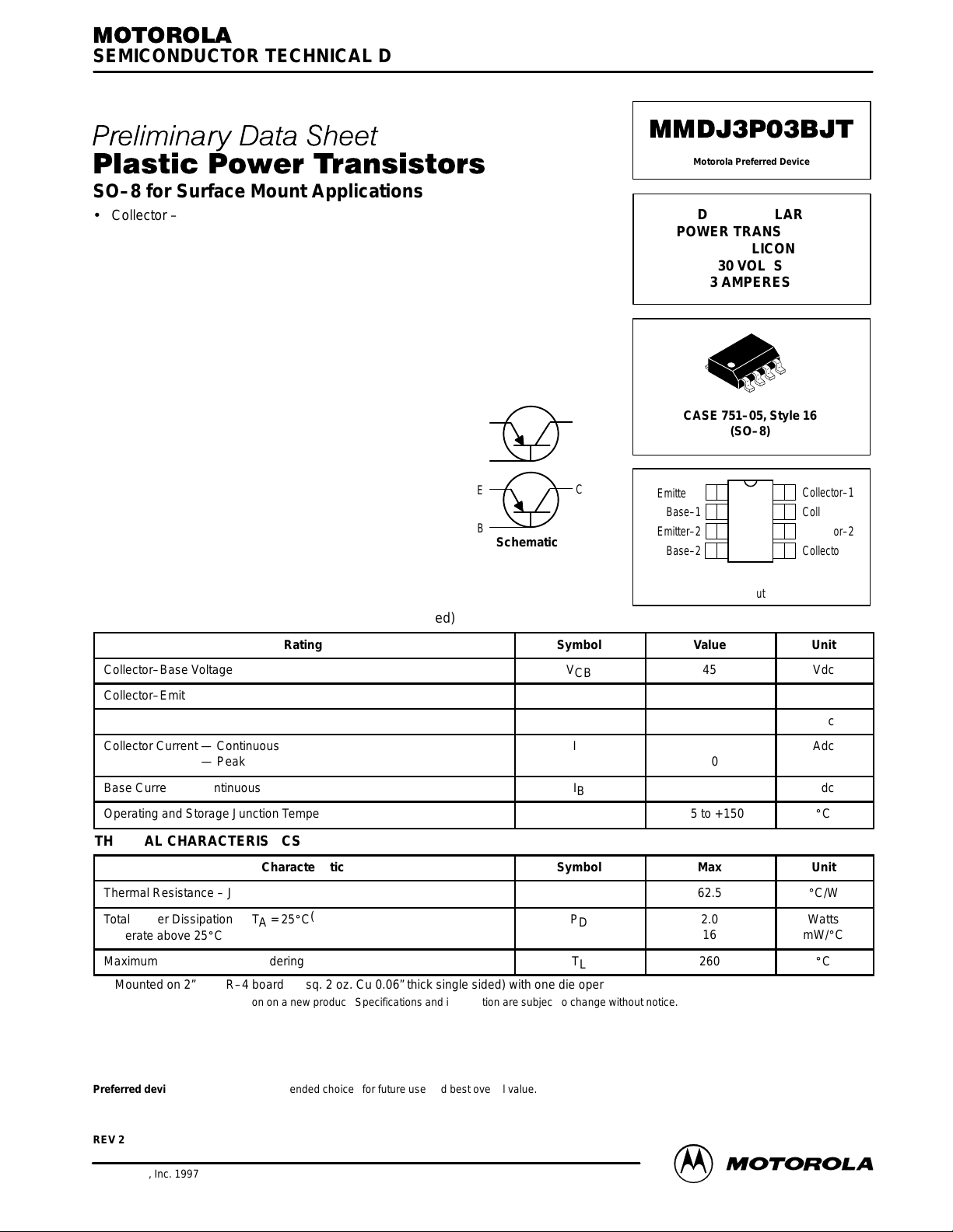
SO–8 for Surface Mount Applications
• Collector –Emitter Sustaining Voltage — V
CEO(sus)
= 30 Vdc (Min) @ IC = 10 mAdc
• High DC Current Gain — h
FE
= 140 (Min) @ IC = 1.2 Adc
= 125 (Min) @ IC = 3.0 Adc
• Low Collector –Emitter Saturation Voltage — V
CE(sat)
= 0.24 Vdc (Max) @ IC = 1.2 Adc
= 0.60 Vdc (Max) @ IC = 5.0 Adc
• Miniature SO–8 Surface Mount Package – Saves Board Space
E
B
E
B
Schematic
C
C
MAXIMUM RATINGS (TC = 25°C unless otherwise noted)
Rating
Collector–Base Voltage
Collector–Emitter Voltage
Emitter–Base Voltage
Collector Current — Continuous
ООООООООООООООООО
Collector Current — Peak
Base Current — Continuous
Operating and Storage Junction Temperature Range
Symbol
V
CB
V
CEO
V
EB
I
I
TJ, T
C
B
stg
ООООО
ООООО
THERMAL CHARACTERISTICS
Characteristic
Thermal Resistance – Junction to Ambient
ООООООООООООООООО
Total Power Dissipation @ TA = 25_C
ООООООООООООООООО
Derate above 25_C
(1)
(1)
Maximum T emperature for Soldering
(1) Mounted on 2” sq. FR–4 board (1” sq. 2 oz. Cu 0.06” thick single sided) with one die operating, 10 seconds max.
This document contains information on a new product. Specifications and information are subject to change without notice.
Symbol
R
ООООО
ООООО
θJC
P
T
D
L
ООООО
ООООО
DUAL BIPOLAR
POWER TRANSISTOR
PNP SILICON
30 VOLTS
3 AMPERES
CASE 751–05, Style 16
Emitter–1
Base–1
Emitter–2
Base–2
Value
45
30
± 8.0
3.0
5.0
1.0
–55 to +150
Max
62.5
2.0
16
260
(SO–8)
1
2
3
4
Top View
Pinout
8
7
6
5
ÎÎÎ
ÎÎÎ
ÎÎÎ
Collector–1
Collector–1
Collector–2
Collector–2
Unit
Vdc
Vdc
Vdc
Adc
Adc
_
C
Unit
_
C/W
Watts
mW/_C
_
C
Preferred devices are Motorola recommended choices for future use and best overall value.
REV 2
Motorola, Inc. 1997
Motorola Bipolar Power Transistor Device Data
1
Page 2
MMDJ3P03BJT
ÎÎÎ
Î
Î
Î
Î
Î
ÎÎÎ
Î
Î
Î
Î
Î
Î
ÎÎÎ
Î
Î
Î
Î
Î
Î
ÎÎÎ
Î
Î
Î
Î
Î
Î
Î
Î
Î
Î
Î
ÎÎÎ
Î
Î
Î
Î
Î
Î
Î
ÎÎÎ
Î
ÎÎÎ
Î
Î
Î
Î
Î
Î
Î
Î
Î
Î
ÎÎÎ
Î
Î
Î
Î
Î
Î
Î
ÎÎÎ
Î
Î
Î
Î
Î
Î
ÎÎÎ
Î
Î
Î
Î
Î
Î
ÎÎÎ
Î
ELECTRICAL CHARACTERISTICS (T
Characteristic
OFF CHARACTERISTICS
ОООООООООООООООООООООООООООООООО
Collector–Emitter Sustaining Voltage
ОООООООООООООООООО
(IC = 10 mAdc, IB = 0 Adc)
Collector Cutoff Current
ОООООООООООООООООО
(VCE = 25 Vdc, RBE = 200 W)
Emitter Cutoff Current
(VBE = 5.0 Vdc)
ОООООООООООООООООО
ON CHARACTERISTICS
Collector–Emitter Saturation Voltage
(IC = 0.8 Adc, IB = 20 mAdc)
ОООООООООООООООООО
(IC = 1.2 Adc, IB = 20 mAdc)
(IC = 5.0 Adc, IB = 1.0 Adc)
ОООООООООООООООООО
Base–Emitter Saturation Voltage
(IC = 5.0 Adc, IB = 1.0 Adc)
ОООООООООООООООООО
Base–Emitter On Voltage
(IC = 3.0 Adc, VCE = 4.0 Vdc)
DC Current Gain
ОООООООООООООООООО
(IC = 1.2 Adc, VCE = 4.0 Vdc)
(IC = 3.0 Adc, VCE = 4.0 Vdc)
ОООООООООООООООООО
(1)
= 25_C unless otherwise noted)
C
Symbol
V
CEO(sus)
ÎÎ
I
CER
ÎÎ
I
EBO
ÎÎ
V
CE(sat)
ÎÎ
ÎÎ
V
BE(sat)
ÎÎ
V
BE(on)
h
FE
ÎÎ
ÎÎ
Min
ÎÎ
30
ÎÎ
—
—
ÎÎ
—
ÎÎ
—
—
ÎÎ
—
ÎÎ
—
ÎÎ
140
125
ÎÎ
Typ
ÎÎ
—
ÎÎ
—
—
ÎÎ
0.14
ÎÎ
—
—
ÎÎ
—
ÎÎ
—
ÎÎ
—
180
ÎÎ
Max
ÎÎ
—
ÎÎ
20
10
ÎÎ
0.20
ÎÎ
0.24
0.60
ÎÎ
1.40
ÎÎ
1.10
ÎÎ
—
—
ÎÎ
Unit
Vdc
ÎÎ
µAdc
ÎÎ
µAdc
ÎÎ
Vdc
ÎÎ
ÎÎ
Vdc
ÎÎ
Vdc
—
ÎÎ
ÎÎ
DYNAMIC CHARACTERISTICS
Output Capacitance
(VCB = 10 Vdc, IE = 0 Adc, f = 1.0 MHz)
ОООООООООООООООООО
Input Capacitance
ОООООООООООООООООО
(VEB = 8.0 Vdc)
Current–Gain — Bandwidth Product
ОООООООООООООООООО
(IC = 500 mA, VCE = 10 V, F
(2)
= 1.0 MHz)
test
C
ob
ÎÎ
C
ib
ÎÎ
f
T
ÎÎ
—
ÎÎ
ÎÎ
—
ÎÎ
—
100
ÎÎ
ÎÎ
135
ÎÎ
105
—
ÎÎ
ÎÎ
—
ÎÎ
—
pF
ÎÎ
pF
ÎÎ
MHz
ÎÎ
(1) Pulse Test: Pulse Width ≤ 300 µs, Duty Cycle ≤ 2%.
(2) fT = |hFE| S f
test
2
Motorola Bipolar Power Transistor Device Data
Page 3

MMDJ3P03BJT
1000
100
, DC CURRENT GAIN
FE
h
1.00
0.75
0.50
10
1.0
VCE = 2 V
1.0
150°C
25°C
–55°C
0.1
V, VOLTAGE (V)
0.1 0.1
IC, COLLECTOR CURRENT (A)
1.0 100.01
0.01
V
BE(sat)
V
CE(sat)
IC/IB = 125
1.0 100.01
IC, COLLECTOR CURRENT (A)
Figure 1. DC Current Gain Figure 2. “ON” Voltages
1000
IC = 1.2 AIC = 0.8 A
C
100
ob
0.25
, COLLECTOR–EMITTER VOL TAGE (V)
CE(sat)
V
, EFFECTIVE TRANSIENT
thja(t)
R
0
1.0
0.1
THERMAL RESISTANCE
0.01
0.001
IC = 0.5 A
10
0.00001
CAPACITANCE (pF)
10
IB, BASE CURRENT (mA)
1001.0
10
1.00.1
VR, REVERSE BIAS (V)
10 100
Figure 3. Collector Saturation Region Figure 4. Capacitance
D = 0.5
0.2
0.1
0.05
0.02
0.01
CHIP
JUNCTION
SINGLE PULSE
IC, COLLECTOR CURRENT (AMPS)
NORMALIZED TO
W
0.0106
0.0253 F 0.1406 F 0.5064 F 2.9468 F
0.0431 W0.1643 W0.3507 W0.4302
q
ja AT 10 s
W
177.14 F
AMBIENT
10000.0001 0.001 0.01 0.1 1.0 10 100
Motorola Bipolar Power Transistor Device Data
Figure 5. Thermal Response
3
Page 4

MMDJ3P03BJT
P ACKAGE DIMENSIONS
–T–
–B–
–A–
M
B
58
1
4
M
4X P
J
_
X 45
R
0.25 (0.010)
_
M
G
F
C
SEATING
K
8X D
PLANE
SS
A0.25 (0.010)MTB
NOTES:
1. DIMENSIONS A AND B ARE DATUMS AND T IS A
DATUM SURFACE.
2. DIMENSIONING AND TOLERANCING PER ANSI
Y14.5M, 1982.
3. DIMENSIONS ARE IN MILLIMETER.
4. DIMENSION A AND B DO NOT INCLUDE MOLD
PROTRUSION.
5. MAXIMUM MOLD PROTRUSION 0.15 PER SIDE.
6. DIMENSION D DOES NOT INCLUDE MOLD
PROTRUSION. ALLOWABLE DAMBAR
PROTRUSION SHALL BE 0.127 TOTAL IN EXCESS
OF THE D DIMENSION AT MAXIMUM MATERIAL
CONDITION.
MILLIMETERS
DIM MIN MAX
A 4.80 5.00
B 3.80 4.00
C 1.35 1.75
D 0.35 0.49
F 0.40 1.25
G 1.27 BSC
J 0.18 0.25
K 0.10 0.25
M 0 7
P 5.80 6.20
R 0.25 0.50
STYLE 16:
PIN 1. EMITTER, DIE #1
__
2. BASE, DIE #1
3. EMITTER, DIE #2
4. BASE, DIE #2
5. COLLECTOR, DIE #2
6. COLLECTOR, DIE #2
7. COLLECTOR, DIE #1
8. COLLECTOR, DIE #1
CASE 751–05
ISSUE P
Motorola reserves the right to make changes without further notice to any products herein. Motorola makes no warranty , representation or guarantee regarding
the suitability of its products for any particular purpose, nor does Motorola assume any liability arising out of the application or use of any product or circuit, and
specifically disclaims any and all liability, including without limitation consequential or incidental damages. “T ypical” parameters which may be provided in Motorola
data sheets and/or specifications can and do vary in different applications and actual performance may vary over time. All operating parameters, including “Typicals”
must be validated for each customer application by customer’s technical experts. Motorola does not convey any license under its patent rights nor the rights of
others. Motorola products are not designed, intended, or authorized for use as components in systems intended for surgical implant into the body, or other
applications intended to support or sustain life, or for any other application in which the failure of the Motorola product could create a situation where personal injury
or death may occur. Should Buyer purchase or use Motorola products for any such unintended or unauthorized application, Buyer shall indemnify and hold Motorola
and its officers, employees, subsidiaries, affiliates, and distributors harmless against all claims, costs, damages, and expenses, and reasonable attorney fees
arising out of, directly or indirectly, any claim of personal injury or death associated with such unintended or unauthorized use, even if such claim alleges that
Motorola was negligent regarding the design or manufacture of the part. Motorola and are registered trademarks of Motorola, Inc. Motorola, Inc. is an Equal
Opportunity/Affirmative Action Employer.
Mfax is a trademark of Motorola, Inc.
How to reach us:
USA/EUROPE/Locations Not Listed: Motorola Literature Distribution; JAPAN: Nippon Motorola Ltd.; Tatsumi–SPD–JLDC, 6F Seibu–Butsuryu–Center,
P.O. Box 5405, Denver, Colorado 80217. 303–675–2140 or 1–800–441–2447 3–14–2 T atsumi Koto–Ku, Tokyo 135, Japan. 81–3–3521–8315
Mfax: RMFAX0@email.sps.mot.com – TOUCHTONE 602–244–6609 ASIA/PACIFIC: Motorola Semiconductors H.K. Ltd.; 8B Tai Ping Industrial Park,
– US & Canada ONLY 1–800–774–1848 51 Ting Kok Road, Tai Po, N.T ., Hong Kong. 852–26629298
INTERNET: http://www.mot.com/SPS/
4
◊
Motorola Bipolar Power Transistor Device Data
MMDJ3P03BJT/D
 Loading...