

Page 1
1
Motorola TMOS Product Preview Data
FETKY
MOSFET and Schottky Rectifier
The FETKY product family incorporates low R
DS(on)
, true logic level MOSFETs
packaged with industry leading, low forward drop, low leakage Schottky Barrier rectifiers
to offer high efficiency components in a space saving configuration. Independent pinouts
for TMOS and Schottky die allow the flexibility to use a single component for switching
and rectification functions in a wide variety of applications such as Buck Converter,
Buck–Boost, Synchronous Rectification, Low Voltage Motor Control, and Load Management in Battery Packs, Chargers, Cell Phones and other Portable Products.
• HDTMOS Power MOSFET with Low V
F
, Low IR Schottky Rectifier
• Lower Component Placement and Inventory Costs along with
Board Space Savings
• Logic Level Gate Drive — Can be Driven by Logic ICs
• Mounting Information for SO–8 Package Provided
• I
DSS
Specified at Elevated Temperature
• Applications Information Provided
MOSFET MAXIMUM RATINGS
(TJ = 25°C unless otherwise noted)
(1)
Rating
Symbol Value Unit
Drain–to–Source Voltage V
DSS
20 Vdc
Drain–to–Gate Voltage (RGS = 1.0 MW)
V
DGR
20 Vdc
Gate–to–Source Voltage — Continuous V
GS
"
20 Vdc
Drain Current
(3)
— Continuous @ TA = 25°C
— Continuous @ TA = 100°C
— Single Pulse (tp v 10 ms)
I
D
I
D
I
DM
3.3
2.1
20
Adc
Apk
Total Power Dissipation @ TA = 25°C
(2)
P
D
2.0 Watts
Single Pulse Drain–to–Source Avalanche Energy — STAR TING TJ = 25°C
VDD = 30 Vdc, VGS = 5.0 Vdc, VDS = 20 Vdc, IL = 9.0 Apk, L = 10 mH, RG = 25
W
E
AS
324 mJ
SCHOTTKY RECTIFIER MAXIMUM RATINGS (T
J
= 25°C unless otherwise noted)
Peak Repetitive Reverse Voltage
DC Blocking Voltage
V
RRM
V
R
20 Volts
Average Forward Current
(3)
(Rated VR) TA = 100°C I
O
1.0 Amps
Peak Repetitive Forward Current
(3)
(Rated VR, Square Wave, 20 kHz) TA = 105°C I
frm
2.0 Amps
Non–Repetitive Peak Surge Current
(Surge applied at rated load conditions, halfwave, single phase, 60 Hz)
I
fsm
20 Amps
DEVICE MARKING ORDERING INFORMATION
Device Reel Size Tape Width Quantity
2P102
MMDFS2P102R2 13″ 12 mm embossed tape 2500 units
(1) Negative sign for P–channel device omitted for clarity.
(2) Pulse Test: Pulse Width ≤ 250 µs, Duty Cycle ≤ 2.0%.
(3) Mounted on 2″ square FR4 board (1″ sq. 2 oz. Cu 0.06″ thick single sided), 10 sec. max.
Designer’s Data for “Worst Case” Conditions— The Designer’s Data Sheet permits the design of most circuits entirely from the information presented. SOA Limit
curves — representing boundaries on device characteristics — are given to facilitate “worst case” design.
HDTMOS and Designer’s are trademarks of Motorola, Inc. TMOS is a registered trademark of Motorola, Inc.
FETKY is a trademark of International Rectifier.
Order this document
by MMDFS2P102/D
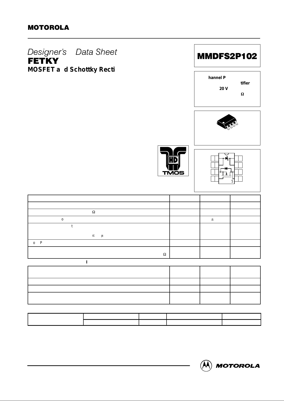
MOTOROLA
SEMICONDUCTOR TECHNICAL DATA
MMDFS2P102
P–Channel Power MOSFET
with Schottky Rectifier
20 Volts
R
DS(on)
= 0.16
W
VF = 0.39 Volts
CASE 751–05, Style 18
(SO–8)
1
2
3
4
8
7
6
5
A
A
S
G
C
C
D
D
TOP VIEW
Motorola, Inc. 1997
Page 2
MMDFS2P102
2
Motorola TMOS Product Preview Data
THERMAL CHARACTERISTICS — SCHOTTKY AND MOSFET
Thermal Resistance — Junction–to–Ambient
(1)
— MOSFET
R
q
JA
167
°C/W
Thermal Resistance — Junction–to–Ambient
(2)
— MOSFET
R
q
JA
100
Thermal Resistance — Junction–to–Ambient
(3)
— MOSFET
R
q
JA
62.5
Thermal Resistance — Junction–to–Ambient
(1)
— Schottky
R
q
JA
204
Thermal Resistance — Junction–to–Ambient
(2)
— Schottky
R
q
JA
122
Thermal Resistance — Junction–to–Ambient
(3)
— Schottky
R
q
JA
83
Operating and Storage Temperature Range Tj, T
stg
–55 to 150
(1) Mounted with minimum recommended pad size, PC Board FR4.
(2) Mounted on 2″ square FR4 board (1″ sq. 2 oz. Cu 0.06″ thick single sided), Steady State.
(3) Mounted on 2″ square FR4 board (1″ sq. 2 oz. Cu 0.06″ thick single sided), 10 sec. max.
Page 3
MMDFS2P102
3
Motorola TMOS Product Preview Data
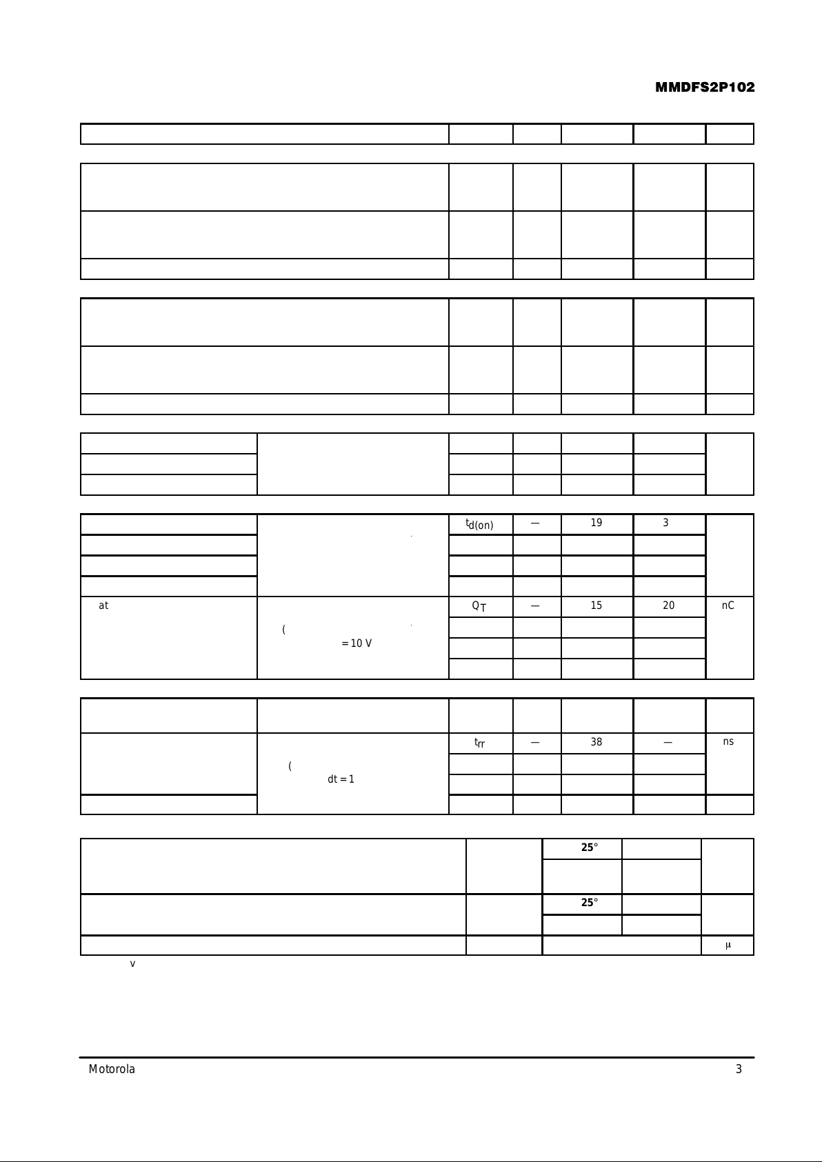
MOSFET ELECTRICAL CHARACTERISTICS (T
J
= 25°C unless otherwise noted)
(1)
Characteristic
Symbol Min Typ Max Unit
OFF CHARACTERISTICS
Drain–Source Voltage
(VGS = 0 Vdc, ID = 0.25 mA)
T emperature Coef ficient (Positive)
V
(BR)DSS
20
—
—
25
—
—
Vdc
mV/°C
Zero Gate Drain Current
(VDS = 30 Vdc, VGS = 0 Vdc)
(VDS = 20 Vdc, VGS = 0 Vdc, TJ = 125°C)
I
DSS
—
—
—
—
1.0
10
µAdc
Gate Body Leakage Current (VGS = ± 20 Vdc, VDS = 0) I
GSS
— — 100 nAdc
ON CHARACTERISTICS
(2)
Gate Threshold Voltage
(VDS = VGS, ID = 0.25 mA)
T emperature Coef ficient (Negative)
V
GS(th)
1.0
—
1.5
4.0
2.0
—
Vdc
mV/°C
Static Drain–Source Resistance
(VGS = 10 Vdc, ID = 2.0 Adc)
(VGS = 4.5 Vdc, ID = 2.5 Adc)
R
DS(on)
—
—
0.118
0.152
0.160
0.180
Ohms
Forward Transconductance (VDS = 3.0 Vdc, ID = 1.0 Adc) g
FS
2.0 3.0 — mhos
DYNAMIC CHARACTERISTICS
Input Capacitance
C
iss
— 420 588 pF
Output Capacitance
(VDS = 16 Vdc, VGS = 0 Vdc,
f = 1.0 MHz
)
C
oss
— 290 406
Reverse Transfer Capacitance
f = 1.0 MHz)
C
rss
— 116 232
SWITCHING CHARACTERISTICS
(3)
Turn–On Delay Time
t
d(on)
— 19 38 ns
Rise Time
(VDS = 10 Vdc, ID = 2.0 Adc,
t
r
— 66 132
Turn–Off Delay Time
V
GS
= 4.5 Vdc,
RG = 6.0 Ω)
t
d(off)
— 25 50
Fall Time
G
)
t
f
— 37 74
Gate Charge
Q
T
— 15 20
nC
(VDS = 16 Vdc, ID = 2.0 Adc,
Q
1
— 1.2 —
(
DS
,
D
,
VGS = 10 Vdc)
Q
2
— 5.0 —
Q
3
— 4.0 —
DRAIN SOURCE DIODE CHARACTERISTICS
Forward On–Voltage
(2)
(IS = 2.0 Adc,
VGS = 0 Vdc)
V
SD
— 1.5 2.1
V
Reverse Recovery Time
t
rr
— 38 —
ns
(IS = 2.0 Adc, VDD = 15 V,
t
a
— 17 —
(
S
,
DD
,
dIS/dt = 100 A/µs)
t
b
— 21 —
Reverse Recovery Stored Charge Q
RR
— 0.034 — µC
SCHOTTKY RECTIFIER ELECTRICAL CHARACTERISTICS (T
J
= 25°C unless otherwise noted)
Maximum Instantaneous Forward Voltage
(2)
V
F
TJ = 25°C TJ = 125°C
Volts
IF = 1.0 A
IF = 2.0 A
0.47
0.58
0.39
0.53
Maximum Instantaneous Reverse Current
(2)
I
R
TJ = 25°C TJ = 125°C
mA
VR = 20 V
0.05 10
Maximum Voltage Rate of Change VR = 20 V dV/dt 10,000
V/ms
(1) Negative sign for P–channel device omitted for clarity.
(2) Pulse Test: Pulse Width ≤ 300 µsec, Duty Cycle ≤ 2.0%.
(3) Switching characteristics are independent of operating temperature.
Page 4
MMDFS2P102
4
Motorola TMOS Product Preview Data
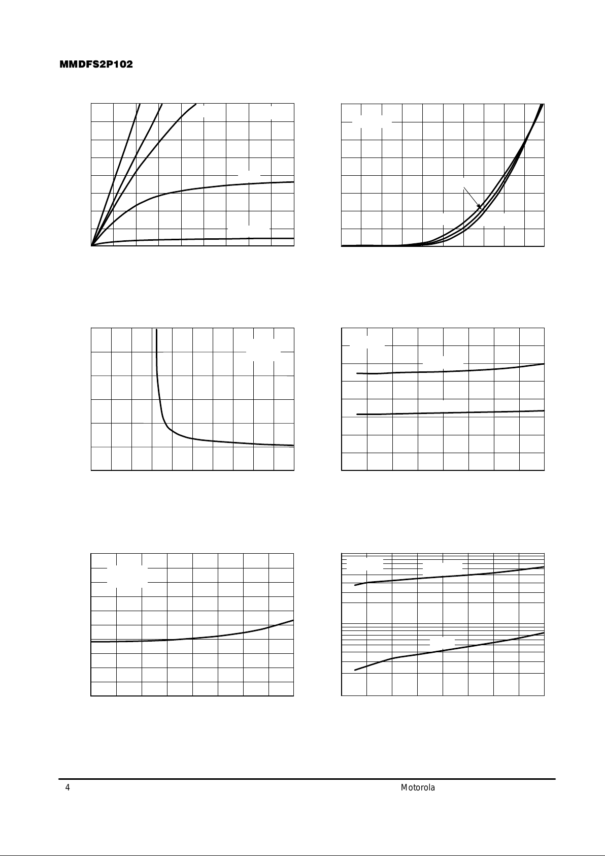
TYPICAL FET ELECTRICAL CHARACTERISTICS
Figure 1. On–Region Characteristics Figure 2. Transfer Characteristics
Figure 3. On–Resistance versus
Gate–T o–Source Voltage
Figure 4. On–Resistance versus Drain Current
and Gate Voltage
Figure 5. On–Resistance Variation with
Temperature
Figure 6. Drain–To–Source Leakage
Current versus Voltage
1.20
VDS, DRAIN–TO–SOURCE VOL TAGE (VOLTS)
4.0
3.0
2.0
VGS, GATE–T O–SOURCE VOLT AGE (VOLTS)
3.51.0
3.0
2.0
1.0
0
8.0 100
VGS, GATE–T O–SOURCE VOLT AGE (VOLTS)
0.6
0.4
0.3
0.2
0.1
0
ID, DRAIN CURRENT (AMPS)
0.50
0.20
0.16
0.12
0.08
0.04
1.0
–25 25–50
TJ, JUNCTION TEMPERATURE (
°
C)
1.2
0.8
0.6
VDS, DRAIN–TO–SOURCE VOL TAGE (VOLTS)
5.0 200
100
1.0
150
I
D
, DRAIN CURRENT (AMPS)
I
R
1.0
0
0.60.2 0.4 0.8 1.0 1.4 1.6 1.5 2.0 2.5 3.0
4.0
2.0 4.0 6.0 1.5 2.0 2.5 3.0 3.5 4.0
, DRAIN–TO–SOURCE RESIST ANCE (NORMALIZED)R
DS(on)
50 10075
1.0
10
10
I
DSS
, LEAKAGE (nA)
1.8
, DRAIN CURRENT (AMPS)
D
, DRAIN–TO–SOURCE RESIST ANCE (OHMS)
DS(on)
0.5
R , DRAIN–TO–SOURCE RESIST ANCE (OHMS)
DS(on)
125 150
1.4
1.6
VGS = 10 V
ID = 2.0 A
VGS = 0 V
TJ = 125°C
100°C
TJ = 25°C
VGS = 4.5 V
10 V
TJ = 25°C
ID = 1.0 A
VDS ≥ 10 V
TJ = –55°C
100°C
25°C
TJ = 25°C
3.1 V
VGS = 2.4 V
10 V
4.5 V
3.8 V
Page 5

MMDFS2P102
5
Motorola TMOS Product Preview Data
TYPICAL FET ELECTRICAL CHARACTERISTICS
Mounted on 2″ sq. FR4 board (1″ sq. 2 oz. Cu 0.06
″
thick single sided) with one die operating, 10 s max.
Figure 7. Capacitance Variation
Figure 8. Gate–To–Source and
Drain–To–Source Voltage versus Total Charge
Figure 9. Resistive Switching Time Variation
versus Gate Resistance
Figure 10. Diode Forward Voltage versus
Current
Figure 11. Maximum Rated Forward Biased
Safe Operating Area
Figure 12. Maximum Avalanche Energy versus
Starting Junction Temperature
5.0 20–10
GATE–T O–SOURCE OR DRAIN–TO–SOURCE VOLT AGE (VOLTS)
1200
800
1000
600
QG, TOTAL GATE CHARGE (nC)
160
6.0
4.0
2.0
0
1001.0
RG, GATE RESISTANCE (OHMS)
1000
100
10
VSD, SOURCE–TO–DRAIN VOL TAGE (VOLTS)
0.5
2.0
1.6
1.2
0.8
0.4
0
0.7
0.1
VDS, DRAIN–TO–SOURCE VOL TAGE (VOLTS)
0.1
0.01
TJ, STARTING JUNCTION TEMPERATURE (
°
C)
50 15025
350
300
50
0
1.0
C, CAPACITANCE (pF)
V
400
200
0
–5.0 0 10 4.0 8.0 12
12
10 0.9 1.1 1.3 1.5
, DRAIN CURRENT (AMPS)I
D
10
1.0
75 100 125
100
E
AS
, SINGLE PULSE DRAIN–TO–SOURCE
15
, GATE–T O–SOURCE VOLT AGE (VOLTS)
GS
t, TIME (ns)
I , SOURCE CURRENT (AMPS)
S
100
10
100
10
8.0
150
200
250
AVALANCHE ENERGY (mJ)
ID = 6.0 A
VDS = 0 VGS = 0
TJ = 25°C
VGS = 0 V
TJ = 25
°
C
C
iss
C
iss
C
oss
C
rss
C
rss
ID = 2.0 A
TJ = 25°C
V
DS
V
GS
Q
T
Q2Q1
Q3
t
d(off)
t
d(on)
t
r
t
f
R
DS(on)
LIMIT
THERMAL LIMIT
PACKAGE LIMIT
dc
10 ms
1.0 ms
100 ms
10 ms
VGS = 20 V
SINGLE PULSE
TC = 25
°
C
VGSV
DS
0
18
16
14
12
10
8.0
6.0
4.0
2.0
Page 6

MMDFS2P102
6
Motorola TMOS Product Preview Data
TYPICAL FET ELECTRICAL CHARACTERISTICS
Figure 13. FET Thermal Response
Figure 14. Diode Reverse Recovery Waveform
di/dt
t
rr
t
a
t
p
I
S
0.25 I
S
TIME
I
S
t
b
t, TIME (s)
Rthja(t), EFFECTIVE TRANSIENT
THERMAL RESPONSE
1.0
0.1
0.001
D = 0.5
SINGLE PULSE
1.0E–05 1.0E–04 1.0E–03 1.0E–02 1.0E–01 1.0E+00 1.0E+01
0.2
0.1
0.05
0.02
0.01
1.0E+02 1.0E+03
0.0001
0.01
NORMALIZED TO R
q
JA
AT STEADY STATE (1″ PAD)
CHIP
JUNCTION
0.0175
W
0.0154 F
0.0710
W
0.0854 F
0.2706
W
0.3074 F
0.5776
W
1.7891 F
0.7086
W
107.55 F
AMBIENT
TYPICAL SCHOTTKY ELECTRICAL CHARACTERISTICS
TJ = 125°C
Figure 15. Typical Forward Voltage Figure 16. Maximum Forward Voltage
0.7 1.00.1
VF, INSTANTANEOUS FORWARD VOLTAGE (VOLTS)
10
1.0
VF, MAXIMUM INSTANTANEOUS FORWARD VOLTAGE (VOL TS)
1.40
1.0
0.1
I
F
, INSTANTANEOUS FORWARD CURRENT (AMPS)
0.1
0.40.2 0.3 0.5 0.6 0.8 0.9 0.2 0.4 0.6 0.8
10
I
F
, INSTANTANEOUS FORWARD CURRENT (AMPS)
1.0 1.2
85°C 25°C
–40°C
TJ = 125°C
25°C
85°C
Page 7

MMDFS2P102
7
Motorola TMOS Product Preview Data
TYPICAL SCHOTTKY ELECTRICAL CHARACTERISTICS
Figure 17. Typical Reverse Current Figure 18. Maximum Reverse Current
Figure 19. Typical Capacitance Figure 20. Current Derating
Figure 21. Forward Power Dissipation
15 200
VR, REVERSE VOLTAGE (VOLTS)
1E–2
1E–4
1E–3
1E–5
15 200
VR, REVERSE VOLTAGE (VOLTS)
1000
100
10
TA, AMBIENT TEMPERATURE (
°
C)
200
1.6
0.8
0.6
0.4
0.2
0
40
0
IO, AVERAGE FORW ARD CURRENT (AMPS)
0.5
0.4
0.3
0.2
0.1
0
0.5
I
R
, REVERSE CURRENT (AMPS)
1E–6
1E–7
5.0 10
5.0 10 60 80 100 120 140 160
, AVERAGE POWER DISSIPA TION (WATTS)P
FO
1.0 1.5
C, CAPACITANCE (pF)
I , AVERAGE FORWARD CURRENT (AMPS)
O
2.0
0.6
0.7
15 200
VR, REVERSE VOLTAGE (VOLTS)
1E–1
1E–3
1E–2
1E–4
I
R
, MAXIMUM REVERSE CURRENT (AMPS)
1E–5
1E–6
5.0 10
1.0
1.2
1.4
SQUARE
WAVE
dc
Ipk/Io = 5.0
Ipk/Io =
p
Ipk/Io = 10
Ipk/Io = 20
TYPICAL CAP ACITANCE A T 0 V = 170 pF
TJ = 125°C
25°C
TJ = 125°C
25°C
85°C
FREQ = 20 kHz
dc
SQUARE WAVE
Ipk/Io = 5.0
Ipk/Io =
p
Ipk/Io = 10
Ipk/Io = 20
Page 8

MMDFS2P102
8
Motorola TMOS Product Preview Data
TYPICAL SCHOTTKY ELECTRICAL CHARACTERISTICS
Figure 22. Schottky Thermal Response
t, TIME (s)
Rthja(t), EFFECTIVE TRANSIENT
THERMAL RESISTANCE
1.0
0.1
D = 0.5
SINGLE PULSE
1.0E–05 1.0E–04 1.0E–03 1.0E–02 1.0E–01 1.0E+00 1.0E+01
0.2
0.1
0.05
0.02
0.01
1.0E+02 1.0E+03
0.001
0.01
NORMALIZED TO R
q
JA
AT STEADY STATE (1″ PAD)
CHIP
JUNCTION
0.0031
W
0.0014 F
0.0154
W
0.0082 F
0.1521
W
0.1052 F
0.4575
W
2.7041 F
0.3719
W
158.64 F
AMBIENT
Page 9

MMDFS2P102
9
Motorola TMOS Product Preview Data
TYPICAL APPLICATIONS
LOAD
V
out
C
O
+
–
V
in
+
–
LOAD
V
out
C
O
+
–
V
in
+
–
L
O
L
O
STEP DOWN SWITCHING REGULA T ORS
Buck Regulator
Synchronous Buck Regulator
LOAD
V
out
C
O
+
–
V
in
+
–
LOAD
V
out
C
O
+
–
V
in
+
–
STEP UP SWITCHING REGULATORS
Boost Regulator
Buck–Boost Regulator
L1
Q1
Page 10

MMDFS2P102
10
Motorola TMOS Product Preview Data
TYPICAL APPLICATIONS
V
in
+
–
MUL TIPLE BATTERY CHARGERS
BATT #1
BATT #2
D2
D3
Q2
Q3
Buck Regulator/Charger
C
O
L
O
Q1
D1
Li–lon BA TTERY PACK APPLICATIONS
Battery Pack
DISCHARGE CHARGE
SMART IC
Li–Ion
BATTERY
CELLS
PACK +
PACK –
SCHOTTKY SCHOTTKY
Q1 Q2
• Applicable in battery packs which require a high current level.
• During charge cycle Q2 is on and Q1 is off. Schottky can reduce power loss during fast charge.
• During discharge Q1 is on and Q2 is off. Again, Schottky can reduce power dissipation.
• Under normal operation, both transistors are on.
Page 11

MMDFS2P102
11
Motorola TMOS Product Preview Data
mm
inches
0.060
1.52
0.275
7.0
0.024
0.6
0.050
1.270
0.155
4.0
SO–8 FOOTPRINT
P ACKAGE DIMENSIONS
CASE 751–05
SO–08
NOTES:
1. DIMENSIONING AND TOLERANCING PER
ANSI Y14.5M, 1982.
2. CONTROLLING DIMENSION: MILLIMETER.
3. DIMENSIONS A AND B DO NOT INCLUDE
MOLD PROTRUSION.
4. MAXIMUM MOLD PROTRUSION 0.15 (0.006)
PER SIDE.
5. DIMENSION D DOES NOT INCLUDE DAMBAR
PROTRUSION. ALLOWABLE DAMBAR
PROTRUSION SHALL BE 0.127 (0.005) TOTAL
IN EXCESS OF THE D DIMENSION AT
MAXIMUM MATERIAL CONDITION.
SEATING
PLANE
14
58
C
K
4X P
A0.25 (0.010)MTB
SS
0.25 (0.010)MB
M
8X D
R
M
J
X 45
_
_
F
–A–
–B–
–T–
DIM MIN MAX MIN MAX
INCHESMILLIMETERS
A 4.80 5.00 0.189 0.196
B 3.80 4.00 0.150 0.157
C 1.35 1.75 0.054 0.068
D 0.35 0.49 0.014 0.019
F 0.40 1.25 0.016 0.049
G 1.27 BSC 0.050 BSC
J 0.18 0.25 0.007 0.009
K 0.10 0.25 0.004 0.009
M 0 7 0 7
P 5.80 6.20 0.229 0.244
R 0.25 0.50 0.010 0.019
____
G
Page 12

MMDFS2P102
12
Motorola TMOS Product Preview Data
Motorola reserves the right to make changes without further notice to any products herein. Motorola makes no warranty , representation or guarantee regarding
the suitability of its products for any particular purpose, nor does Motorola assume any liability arising out of the application or use of any product or circuit, and
specifically disclaims any and all liability, including without limitation consequential or incidental damages. “T ypical” parameters which may be provided in Motorola
data sheets and/or specifications can and do vary in different applications and actual performance may vary over time. All operating parameters, including “Typicals”
must be validated for each customer application by customer’s technical experts. Motorola does not convey any license under its patent rights nor the rights of
others. Motorola products are not designed, intended, or authorized for use as components in systems intended for surgical implant into the body, or other
applications intended to support or sustain life, or for any other application in which the failure of the Motorola product could create a situation where personal injury
or death may occur. Should Buyer purchase or use Motorola products for any such unintended or unauthorized application, Buyer shall indemnify and hold Motorola
and its officers, employees, subsidiaries, affiliates, and distributors harmless against all claims, costs, damages, and expenses, and reasonable attorney fees
arising out of, directly or indirectly, any claim of personal injury or death associated with such unintended or unauthorized use, even if such claim alleges that
Motorola was negligent regarding the design or manufacture of the part. Motorola and are registered trademarks of Motorola, Inc. Motorola, Inc. is an Equal
Opportunity/Affirmative Action Employer.
Mfax is a trademark of Motorola, Inc.
How to reach us:
USA/EUROPE/Locations Not Listed: Motorola Literature Distribution; JAP AN: Nippon Motorola Ltd.; Tatsumi–SPD–JLDC, 6F Seibu–Butsuryu–Center,
P.O. Box 5405, Denver, Colorado 80217. 303–675–2140 or 1–800–441–2447 3–14–2 Tatsumi Koto–Ku, Tokyo 135, Japan. 81–3–3521–8315
Mfax: RMFAX0@email.sps.mot.com – TOUCHTONE 602–244–6609 ASIA/PACIFIC: Motorola Semiconductors H.K. Ltd.; 8B Tai Ping Industrial Park,
– US & Canada ONLY 1–800–774–1848 51 Ting Kok Road, Tai Po, N.T., Hong Kong. 852–26629298
INTERNET: http://motorola.com/sps
MMDFS2P102/D
◊
 Loading...