

Page 1
1
Motorola TMOS Power MOSFET Transistor Device Data
Medium Power Surface Mount Products
WaveFET devices are an advanced series of power MOSFETs which utilize Motorola’s
latest MOSFET technology process to achieve the lowest possible on–resistance per silicon
area. They are capable of withstanding high energy in the avalanche and commutation
modes and the drain–to–source diode has a very low reverse recovery time. WaveFET
devices are designed for use in low voltage, high speed switching applications where power
efficiency is important. Typical applications are dc–dc converters, and power management
in portable and battery powered products such as computers, printers, cellular and cordless
phones. They can also be used for low voltage motor controls in mass storage products
such as disk drives and tape drives. The avalanche energy is specified to eliminate the
guesswork in designs where inductive loads are switched and offer additional safety margin
against unexpected voltage transients.
• Ultra Low R
DS(on)
Provides Higher Efficiency and
Extends Battery Life in Portable Applications
• Characterized Over a Wide Range of Power Ratings
• Logic Level Gate Drive — Can Be Driven by
Logic ICs
• Diode Is Characterized for Use In Bridge Circuits
• Diode Exhibits High Speed, with Soft Recovery
• I
DSS
Specified at Elevated Temperature
• Miniature SO–8 Surface Mount Package —
Saves Board Space
DEVICE MARKING ORDERING INFORMATION
Device Reel Size Tape Width Quantity
D3207
MMDF3207R2 13″ 12 mm embossed tape 2500 units
This document contains information on a product under development. Motorola reserves the right to change or discontinue this product without notice.
HDTMOS is a trademark of Motorola, Inc. TMOS is a registered trademark of Motorola, Inc.
Preferred devices are Motorola recommended choices for future use and best overall value.
Order this document
by MMDF3207/D
SEMICONDUCTOR TECHNICAL DATA
Motorola, Inc. 1997
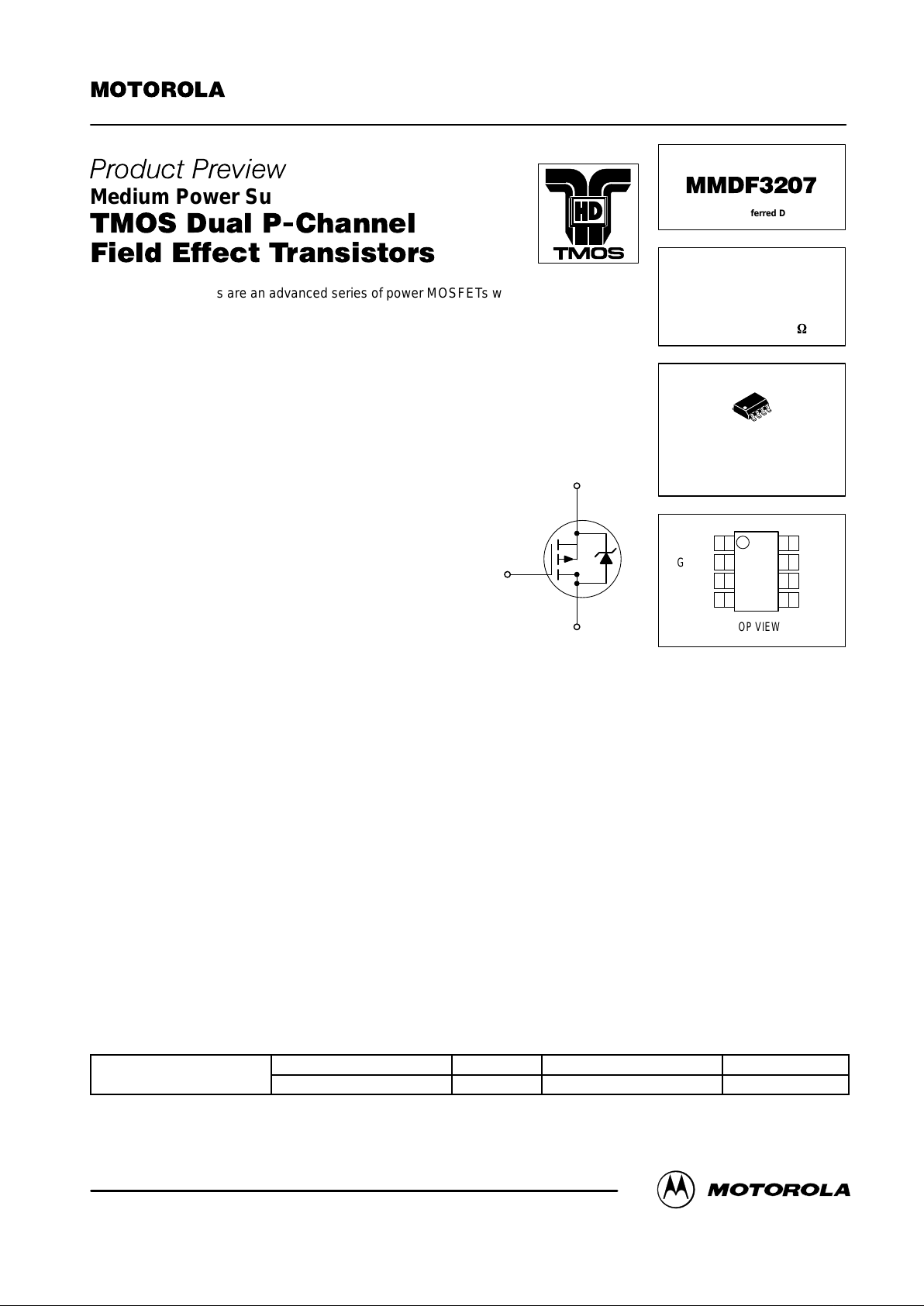
SOURCE 1
TOP VIEW
GATE 1
SOURCE 2
GATE 2
DRAIN 1
DRAIN 1
DRAIN 2
DRAIN 2
CASE 751–06, Style 13
SO–8
DUAL TMOS
POWER MOSFET
7.8 AMPERES
20 VOLTS
R
DS(on)
= 33 m
W
Motorola Preferred Device
S
G
D
1
2
3
4
8
7
6
5
Page 2
MMDF3207
2
Motorola TMOS Power MOSFET Transistor Device Data
MAXIMUM RATINGS
(TJ = 25°C unless otherwise specified)
Characteristics
Symbol Maximum Unit
Drain–to–Source Voltage
Drain–to–Gate Voltage (RGS = 1.0 MW)
Gate–to–Source Voltage — Continuous
V
DSS
V
DGR
V
GS
20
12
±
1
2
V
1 Inch Square @
10 seconds on
FR–4 or G–10 PCB
Thermal Resistance — Junction to Ambient
Total Power Dissipation @ TA = 25°C
Linear Derating Factor
Drain Current — Continuous @ TA = 25°C
Drain Current — Continuous @ TA = 70°C
Drain Current — Pulsed Drain Current
(1)
R
THJA
P
D
I
D
I
D
I
DM
62.5
2.0
16
7.8
5.7
40
°C/W
Watts
mW/°C
A
A
A
1 Inch Square @
Steady State on
FR–4 or G–10 PCB
Thermal Resistance — Junction to Ambient
Total Power Dissipation @ TA = 25°C
Linear Derating Factor
Drain Current — Continuous @ TA = 25°C
Drain Current — Continuous @ TA = 70°C
Drain Current — Pulsed Drain Current
(1)
R
THJA
P
D
I
D
I
D
I
DM
98
1.28
10.2
6.2
4.6
35
°C/W
Watts
mW/°C
A
A
A
Minimum Pad @
Steady State on
FR–4 or G–10 PCB
Thermal Resistance — Junction to Ambient
Total Power Dissipation @ TA = 25°C
Linear Derating Factor
Drain Current — Continuous @ TA = 25°C
Drain Current — Continuous @ TA = 70°C
Drain Current — Pulsed Drain Current
(1)
R
THJA
P
D
I
D
I
D
I
DM
166
0.75
6.0
4.8
3.5
30
°C/W
Watts
mW/°C
A
A
A
Operating and Storage Temperature Range TJ, T
stg
–55 to 150 °C
(1) Repetitive rating; pulse width limited by maximum junction temperature.
Page 3

MMDF3207
3
Motorola TMOS Power MOSFET Transistor Device Data
ELECTRICAL CHARACTERISTICS (T
C
= 25°C unless otherwise noted)
Characteristic Symbol Min Typ Max Unit
OFF CHARACTERISTICS
Drain–to–Source Breakdown Voltage
(1)
(VGS = 0 Vdc, ID = 0.25 mAdc)
T emperature Coef ficient (Positive)
V
(BR)DSS
20
—
—
TBD
—
—
Vdc
mV/°C
Zero Gate Voltage Drain Current
(VDS = 20 Vdc, VGS = 0 Vdc)
(VDS = 20 Vdc, VGS = 0 Vdc, TJ = 55°C)
I
DSS
—
—
—
—
1.0
5.0
µAdc
Gate–Body Leakage Current (VGS = ±12 Vdc, VDS = 0 Vdc) I
GSS
— — 100 nAdc
ON CHARACTERISTICS
(1)
Gate Threshold Voltage
(1)
(VDS = VGS, ID = 0.25 mAdc)
Threshold Temperature Coefficient (Negative)
V
GS(th)
0.6
—
—
TBD
—
—
Vdc
mV/°C
Static Drain–to–Source On–Resistance
(1)
(VGS = 4.5 Vdc, ID = 7.8 Adc)
(VGS = 2.5 Vdc, ID = 6.2 Adc)
R
DS(on)
—
—
TBD
TBD
33
50
mΩ
Forward Transconductance (VDS = 10 Vdc, ID = 7.8 Adc)
(1)
g
FS
— TBD — Mhos
DYNAMIC CHARACTERISTICS
Input Capacitance
C
iss
— TBD TBD pF
Output Capacitance
(VDS = 15 Vdc, VGS = 0 V,
f = 1.0 MHz
)
C
oss
— TBD TBD
Transfer Capacitance
f = 1.0 MHz)
C
rss
— TBD TBD
SWITCHING CHARACTERISTICS
(2)
Turn–On Delay Time
t
d(on)
— TBD TBD
ns
Rise Time
(VDS = 10 Vdc, ID = 1.0 Adc,
t
r
— TBD TBD
Turn–Off Delay Time
V
GS
=
10 Vd
c,
RG = 6.0 Ω)
(1)
t
d(off)
— TBD TBD
Fall Time
G
)
t
f
— TBD TBD
Turn–On Delay Time
t
d(on)
— TBD TBD
Rise Time
(VDD = 10 Vdc, ID = 1.0 Adc,
t
r
— TBD TBD
Turn–Off Delay Time
V
GS
= 4.5 Vdc,
RG = 6.0 Ω)
(1)
t
d(off)
— TBD TBD
Fall Time
G
)
t
f
— TBD TBD
Gate Charge
Q
T
— TBD TBD
nC
(VDS = 10 Vdc, ID = 7.8 Adc,
Q
1
— TBD —
(
DS
,
D
,
VGS = 4.5 Vdc)
(1)
Q
2
— TBD —
Q
3
— TBD —
SOURCE–DRAIN DIODE CHARACTERISTICS
Forward On–Voltage (IS = 1.7 Adc, VGS = 0 Vdc)
(1)
(IS = 1.7 Adc, VGS = 0 Vdc, TJ = 125°C)
V
SD
—
—
TBD
TBD
1.2
—
Vdc
Reverse Recovery Time
t
rr
— TBD —
ns
(IS = 1.7 Adc, VGS = 0 Vdc,
t
a
— TBD —
(
S
,
GS
,
dIS/dt = 100 A/µs)
(1)
t
b
— TBD —
Reverse Recovery Stored Charge Q
RR
— TBD — µC
(1) Pulse Test: Pulse Width ≤ 300 µs, Duty Cycle ≤ 2%.
(2) Switching characteristics are independent of operating junction temperatures.
(3) Repetitive rating; pulse width limited by max. junction temperature.
Page 4

MMDF3207
4
Motorola TMOS Power MOSFET Transistor Device Data
P ACKAGE DIMENSIONS
CASE 751–06
ISSUE T
STYLE 13:
PIN 1. N.C.
2. SOURCE
3. SOURCE
4. GATE
5. DRAIN
6. DRAIN
7. DRAIN
8. DRAIN
SEATING
PLANE
1
4
58
A0.25MCB
SS
0.25MB
M
h
q
C
X 45
_
L
DIM MIN MAX
MILLIMETERS
A 1.35 1.75
A1 0.10 0.25
B 0.35 0.49
C 0.19 0.25
D 4.80 5.00
E
1.27 BSCe
3.80 4.00
H 5.80 6.20
h
0 7
L 0.40 1.25
q
0.25 0.50
__
NOTES:
1. DIMENSIONING AND TOLERANCING PER ASME
Y14.5M, 1994.
2. DIMENSIONS ARE IN MILLIMETER.
3. DIMENSION D AND E DO NOT INCLUDE MOLD
PROTRUSION.
4. MAXIMUM MOLD PROTRUSION 0.15 PER SIDE.
5. DIMENSION B DOES NOT INCLUDE DAMBAR
PROTRUSION. ALLOWABLE DAMBAR
PROTRUSION SHALL BE 0.127 TOTAL IN EXCESS
OF THE B DIMENSION AT MAXIMUM MATERIAL
CONDITION.
D
E
H
A
B
e
B
A1
C
A
0.10
Motorola reserves the right to make changes without further notice to any products herein. Motorola makes no warranty , representation or guarantee regarding
the suitability of its products for any particular purpose, nor does Motorola assume any liability arising out of the application or use of any product or circuit, and
specifically disclaims any and all liability, including without limitation consequential or incidental damages. “T ypical” parameters which may be provided in Motorola
data sheets and/or specifications can and do vary in different applications and actual performance may vary over time. All operating parameters, including “Typicals”
must be validated for each customer application by customer’s technical experts. Motorola does not convey any license under its patent rights nor the rights of
others. Motorola products are not designed, intended, or authorized for use as components in systems intended for surgical implant into the body, or other
applications intended to support or sustain life, or for any other application in which the failure of the Motorola product could create a situation where personal injury
or death may occur. Should Buyer purchase or use Motorola products for any such unintended or unauthorized application, Buyer shall indemnify and hold Motorola
and its officers, employees, subsidiaries, affiliates, and distributors harmless against all claims, costs, damages, and expenses, and reasonable attorney fees
arising out of, directly or indirectly, any claim of personal injury or death associated with such unintended or unauthorized use, even if such claim alleges that
Motorola was negligent regarding the design or manufacture of the part. Motorola and are registered trademarks of Motorola, Inc. Motorola, Inc. is an Equal
Opportunity/Affirmative Action Employer.
Mfax is a trademark of Motorola, Inc.
How to reach us:
USA/EUROPE/Locations Not Listed: Motorola Literature Distribution; JAP AN: Nippon Motorola Ltd.: SPD, Strategic Planning Office, 4–32–1,
P.O. Box 5405, Denver, Colorado 80217. 1–303–675–2140 or 1–800–441–2447 Nishi–Gotanda, Shinagawa–ku, T okyo 141, Japan. 81–3–5487–8488
Customer Focus Center: 1–800–521–6274
Mfax: RMFAX0@email.sps.mot.com – TOUCHTONE 1–602–244–6609 ASIA/PACIFIC: Motorola Semiconductors H.K. Ltd.; 8B Tai Ping Industrial Park,
Moto rola Fax Back System – US & Canada ONLY 1–800–774–1848 51 Ting Kok Road, T ai Po, N.T., Hong Kong. 852–26629298
– http://sps.motorola.com/mfax/
HOME PAGE: http://motorola.com/sps/
MMDF3207/D
◊
 Loading...