

Page 1
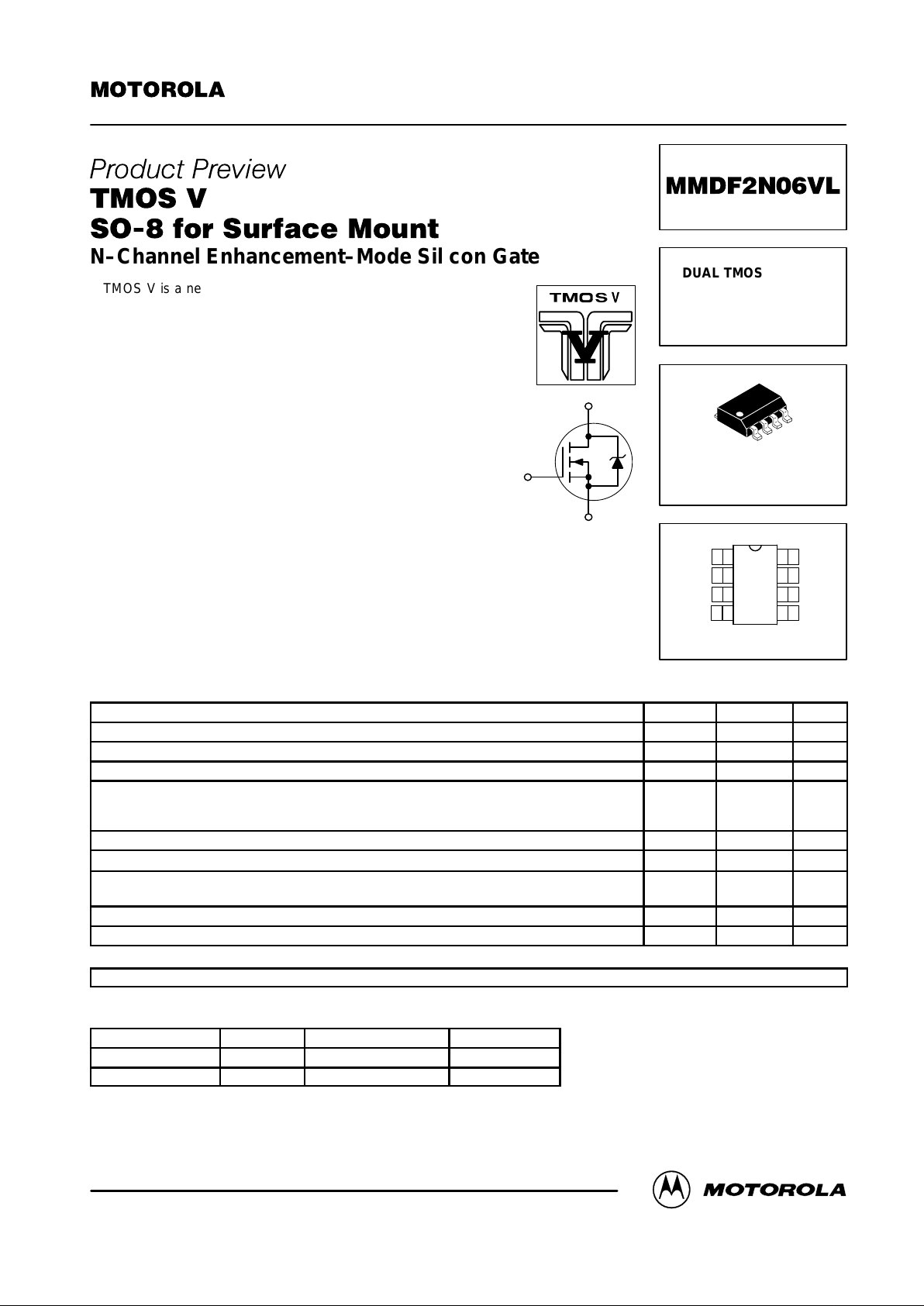
DUAL TMOS MOSFET
2.5 AMPERES
60 VOLTS
R
DS(on)
= 0.130 OHM
Source–1
1
2
3
4
8
7
6
5
Top View
Gate–1
Source–2
Gate–2
Drain–1
Drain–1
Drain–2
Drain–2
D
S
G
CASE 751–05, Style 11
SO–8
TM
1
Motorola TMOS Power MOSFET Transistor Device Data
N–Channel Enhancement–Mode Silicon Gate
TMOS V is a new technology designed to achieve an on–resistance area product about one–half that of standard MOSFET s. This
new technology more than doubles the present cell density of our
50 and 60 volt TMOS devices. Just as with our TMOS E–FET
designs, TMOS V is designed to withstand high energy in the
avalanche and commutation modes. Designed for low voltage, high
speed switching applications in power supplies, converters and
power motor controls, these devices are particularly well suited for
bridge circuits where diode speed and commutating safe operating
areas are critical and offer additional safety margin against
unexpected voltage transients.
New Features of TMOS V
• On–resistance Area Product about One–half that of Standard
MOSFETs with New Low Voltage, Low R
DS(on)
Technology
• Faster Switching than E–FET Predecessors
Features Common to TMOS V and TMOS E–FETS
• Avalanche Energy Specified
• I
DSS
and V
DS(on)
Specified at Elevated Temperature
• Static Parameters are the Same for both TMOS V and TMOS E–FET
• Miniature SO–8 Surface Mount Package – Saves Board Space
• Mounting Information for SO–8 Package Provided
MAXIMUM RATINGS
(TJ = 25°C unless otherwise noted)
Rating
Symbol Value Unit
Drain–to–Source Voltage V
DSS
60 Vdc
Drain–to–Gate Voltage, (RGS = 1 MΩ) V
DGR
60 Vdc
Gate–to–Source Voltage — Continuous V
GS
± 15 Vdc
Drain Current — Continuous @ TA = 25°C
Drain Current — Continuous @ TA = 100°C
Drain Current — Single Pulse (tp ≤ 10 µs)
I
D
I
D
I
DM
2.5
0.5
7.5
Adc
Apk
Total Power Dissipation @ TA = 25°C
(1)
P
D
2.0 W
Operating and Storage Temperature Range TJ, T
stg
–55 to 175 °C
Single Pulse Drain–to–Source Avalanche Energy — Starting TJ = 25°C
(VDD = 25 Vdc, VGS = 5.0 Vdc, Peak IL = 3.3 Apk, L = 10 mH, RG = 25 Ω)
E
AS
54 mJ
Thermal Resistance, Junction to Ambient
(1)
R
θJA
62.5 °C/W
Maximum Lead Temperature for Soldering Purposes, 0.0625″ from case for 10 seconds T
L
260 °C
DEVICE MARKING
2N6VL
(1) Mounted on G10/FR4 glass epoxy board using minimum recommended footprint.
ORDERING INFORMATION
Device Reel Size Tape Width Quantity
MMDF2N06VLR1 7″ 12mm embossed tape 500
MMDF2N06VLR2 13″ 12mm embossed tape 2500
This document contains information on a new product. Specifications and information herein are subject to change without notice.
E–FET and TMOS V are trademarks of Motorola, Inc. TMOS is a registered trademark of Motorola, Inc.
Order this document
by MMDF2N06VL/D
SEMICONDUCTOR TECHNICAL DATA
Motorola, Inc. 1996
Page 2
MMDF2N06VL
2
Motorola TMOS Power MOSFET Transistor Device Data
ELECTRICAL CHARACTERISTICS
(TA = 25°C unless otherwise noted)
Characteristic
Symbol Min Typ Max Unit
OFF CHARACTERISTICS
Drain–to–Source Breakdown Voltage
(VGS = 0 Vdc, ID = 0.25 mAdc)
Temperature Coefficient (Positive)
V
(BR)DSS
60
—
—
66
—
—
Vdc
mV/°C
Zero Gate Voltage Drain Current
(VDS = 60 Vdc, VGS = 0 Vdc)
(VDS = 60 Vdc, VGS = 0 Vdc, TJ = 150°C)
I
DSS
—
—
—
—
10
100
µAdc
Gate–Body Leakage Current (VGS = ± 15 Vdc, VDS = 0 Vdc) I
GSS
— — 100 nAdc
ON CHARACTERISTICS
(1)
Gate Threshold Voltage
(VDS = VGS, ID = 250 µAdc)
Threshold Temperature Coefficient (Negative)
V
GS(th)
1.0
—
1.5
3.0
2.0
—
Vdc
mV/°C
Static Drain–to–Source On–Resistance
(VGS = 5.0 Vdc, ID = 2.5 Adc)
R
DS(on)
— 0.12 0.13
Ohm
Drain–to–Source On–Voltage
(VGS = 5.0 Vdc, ID = 2.5 Adc)
(VGS = 5.0 Vdc, ID = 1.25 Adc, TJ = 150°C)
V
DS(on)
—
—
—
—
0.4
0.3
Vdc
Forward Transconductance (VDS = 15 Vdc, ID = 1.25 Adc) g
FS
1.0 3.0 — Mhos
DYNAMIC CHARACTERISTICS
Input Capacitance
C
iss
— 340 480 pF
Output Capacitance
(VDS = 25 Vdc, VGS = 0 Vdc,
f = 1.0 MHz)
C
oss
— 110 150
Transfer Capacitance
f = 1.0 MHz)
C
rss
— 27 50
SWITCHING CHARACTERISTICS
(2)
Turn–On Delay Time
t
d(on)
— 10 20
ns
Rise Time
(VDD = 30 Vdc, ID = 2.5 Adc,
t
r
— 30 60
Turn–Off Delay Time
VGS = 5.0 Vdc,
RG = 9.1 Ω)
t
d(off)
— 32 60
Fall Time
G
= 9.1 Ω)
t
f
— 28 60
Gate Charge
Q
T
— 11 20 nC
(V
DS
= 48 Vdc, ID = 2.5 Adc,
Q
1
— 1.5 —
(VDS = 48 Vdc, ID = 2.5 Adc,
VGS = 5.0 Vdc)
Q
2
— 3.8 —
Q
3
— 3.5 —
SOURCE–DRAIN DIODE CHARACTERISTICS
Forward On–Voltage
(1)
(IS = 2.5 Adc, VGS = 0 Vdc)
(IS = 2.5 Adc, VGS = 0 Vdc, TJ =
150°C)
V
SD
—
—
0.84
0.67
1.2
—
Vdc
Reverse Recovery Time
t
rr
— 49 —
ns
(I
S
= 2.5 Adc, VGS = 0 Vdc,
t
a
— 32 —
(IS = 2.5 Adc, VGS = 0 Vdc,
dIS/dt = 100 A/µs)
t
b
— 17 —
Reverse Recovery Storage Charge Q
RR
— 0.08 — µC
(1) Pulse Test: Pulse Width ≤ 300 µs, Duty Cycle ≤ 2%.
(2) Switching characteristics are independent of operating junction temperature.
Page 3

MMDF2N06VL
3
Motorola TMOS Power MOSFET Transistor Device Data
PACKAGE DIMENSIONS
STYLE 11:
PIN 1. SOURCE 1
2. GATE 1
3. SOURCE 2
4. GATE 2
5. DRAIN 2
6. DRAIN 2
7. DRAIN 1
8. DRAIN 1
CASE 751–05
SO–8
ISSUE P
SEATING
PLANE
1
4
58
C
K
4X P
A0.25 (0.010)MT B
S S
0.25 (0.010)
M
B
M
8X D
R
M
J
X 45
_
_
F
–A–
–B–
–T–
DIM MIN MAX
MILLIMETERS
A 4.80 5.00
B 3.80 4.00
C 1.35 1.75
D 0.35 0.49
F 0.40 1.25
G 1.27 BSC
J 0.18 0.25
K 0.10 0.25
M 0 7
P 5.80 6.20
R 0.25 0.50
__
G
NOTES:
1. DIMENSIONS A AND B ARE DATUMS AND T IS A
DATUM SURFACE.
2. DIMENSIONING AND TOLERANCING PER ANSI
Y14.5M, 1982.
3. DIMENSIONS ARE IN MILLIMETER.
4. DIMENSION A AND B DO NOT INCLUDE MOLD
PROTRUSION.
5. MAXIMUM MOLD PROTRUSION 0.15 PER SIDE.
6. DIMENSION D DOES NOT INCLUDE MOLD
PROTRUSION. ALLOWABLE DAMBAR
PROTRUSION SHALL BE 0.127 TOTAL IN EXCESS
OF THE D DIMENSION AT MAXIMUM MATERIAL
CONDITION.
Page 4

MMDF2N06VL
4
Motorola TMOS Power MOSFET Transistor Device Data
Motorola reserves the right to make changes without further notice to any products herein. Motorola makes no warranty , representation or guarantee regarding
the suitability of its products for any particular purpose, nor does Motorola assume any liability arising out of the application or use of any product or circuit, and
specifically disclaims any and all liability, including without limitation consequential or incidental damages. “T ypical” parameters which may be provided in Motorola
data sheets and/or specifications can and do vary in different applications and actual performance may vary over time. All operating parameters, including “Typicals”
must be validated for each customer application by customer’s technical experts. Motorola does not convey any license under its patent rights nor the rights of
others. Motorola products are not designed, intended, or authorized for use as components in systems intended for surgical implant into the body, or other
applications intended to support or sustain life, or for any other application in which the failure of the Motorola product could create a situation where personal injury
or death may occur. Should Buyer purchase or use Motorola products for any such unintended or unauthorized application, Buyer shall indemnify and hold Motorola
and its officers, employees, subsidiaries, affiliates, and distributors harmless against all claims, costs, damages, and expenses, and reasonable attorney fees
arising out of, directly or indirectly, any claim of personal injury or death associated with such unintended or unauthorized use, even if such claim alleges that
Motorola was negligent regarding the design or manufacture of the part. Motorola and are registered trademarks of Motorola, Inc. Motorola, Inc. is an Equal
Opportunity/Affirmative Action Employer.
How to reach us:
USA/EUROPE/Locations Not Listed: Motorola Literature Distribution; JAPAN: Nippon Motorola Ltd.; Tatsumi–SPD–JLDC, 6F Seibu–Butsuryu–Center,
P.O. Box 20912; Phoenix, Arizona 85036. 1–800–441–2447 or 602–303–5454 3–14–2 Tatsumi Koto–Ku, Tokyo 135, Japan. 03–81–3521–8315
MFAX: RMFAX0@email.sps.mot.com – TOUCHTONE 602–244–6609 ASIA/PACIFIC: Motorola Semiconductors H.K. Ltd.; 8B Tai Ping Industrial Park,
INTERNET: http://Design–NET.com 51 Ting Kok Road, Tai Po, N.T., Hong Kong. 852–26629298
MMDF2N06VL/D
*MMDF2N06VL/D*
◊
 Loading...