

Page 1
www.vishay.com
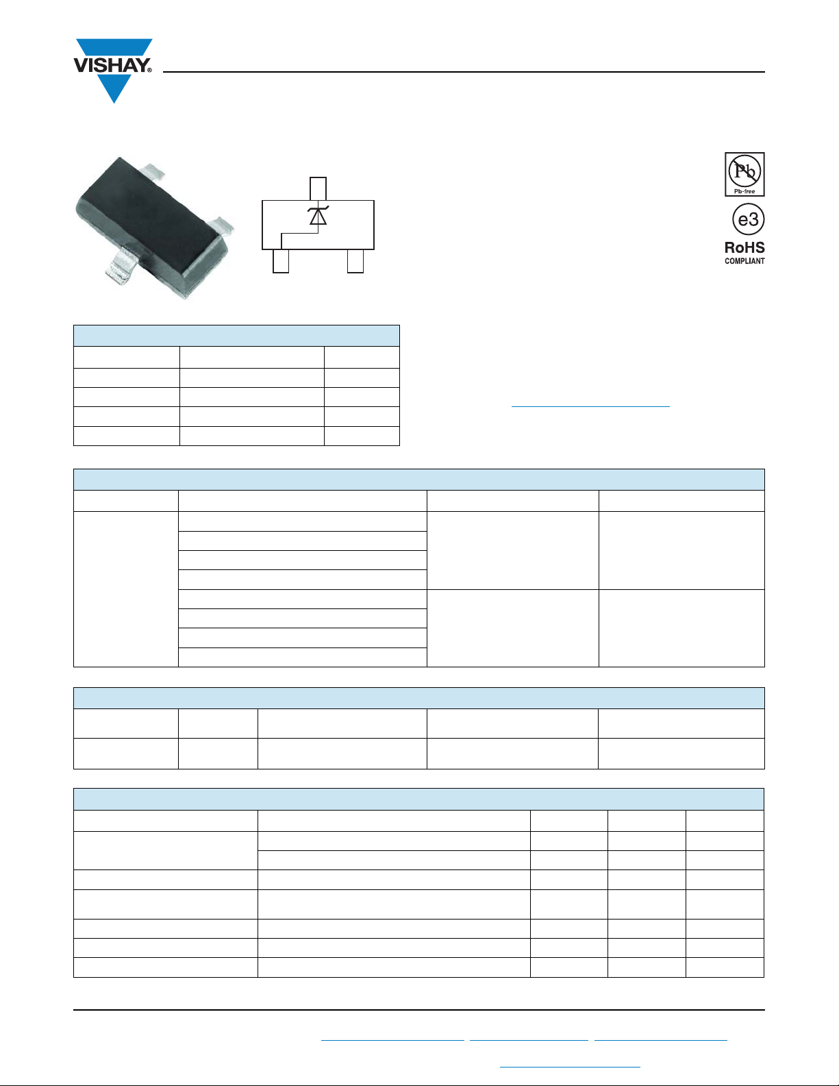
Small Signal Zener Diodes
3
12
PRIMARY CHARACTERISTICS
PARAMETER VALUE UNIT
range nom. 3 to 75 V
V
Z
Test current I
V
specification Thermal equilibrium
Z
Int. construction Single
1.7 to 20 mA
ZT
MMBZ5225 to MMBZ5267
Vishay Semiconductors
FEATURES
• Silicon planar power Zener diodes
• Standard Zener voltage tolerance is ± 5 % with
a “B” suffix (e.g.: MMBZ5225B), suffix “C” is
± 2 % tolerance.
• High temperature soldering guaranteed:
260 °C/4 x 10 s at terminals
• AEC-Q101 qualified
• ESD capability according to AEC-Q101:
Human body model > 8 kV
Machine model > 800 V
• Base P/N-E3 - RoHS-compliant, commercial grade
• Base P/N-HE3 - RoHS-compliant, AEC-Q101 qualified
• Material categorization: For definitions of compliance
please see www.vishay.com/doc?99912
ORDERING INFORMATION
DEVICE NAME ORDERING CODE TAPED UNITS PER REEL MINIMUM ORDER QUANTITY
MMBZ5225B-E3-08 to MMBZ5267B-E3-08
MMBZ5225 to
MMBZ5267
MMBZ5225C-E3-08 to MMBZ5267C-E3-08
MMBZ5225B-HE3-08 to MMBZ5267B-HE3-08
MMBZ5225C-HE3-08 to MMBZ5267C-HE3-08
MMBZ5225B-E3-18 to MMBZ5267B-E3-18
MMBZ5225C-E3-18 to MMBZ5267C-E3-18
MMBZ5225B-HE3-18 to MMBZ5267B-HE3-18
MMBZ5225C-HE3-18 to MMBZ5267C-HE3-18
3000 (8 mm tape on 7" reel) 15 000/box
10 000 (8 mm tape on 13" reel) 10 000/box
PACKAGE
PACKAGE NAME WEIGHT
SOT-23 8.8 mg UL 94 V-0
ABSOLUTE MAXIMUM RATINGS (T
PARAMETER TEST CONDITION SYMBOL VALUE UNIT
Power dissipation
Zener current See table “Electrical Characteristics”
Thermal resistance,
junction to ambient air
Junction temperature
Storage temperature range
Operating temperature range
MOLDING COMPOUND
FLAMMABILITY RATING
= 25 °C, unless otherwise specified)
amb
On FR - 5 board using recommended solder pad layout P
On alumina substrate P
On FR - 5 board using recommended solder pad layout R
MOISTURE SENSITIVITY
LEVEL
MSL level 1
(according J-STD-020)
T
T
tot
tot
thJA
T
stg
op
SOLDERING CONDITIONS
260 °C/10 s at terminals
225 mW
300 mW
556 K/W
j
150 °C
- 65 to + 150 °C
- 55 to + 150 °C
Rev. 1.7, 11-Feb-13
For technical questions within your region: DiodesAmericas@vishay.com
THIS DOCUMENT IS SUBJECT TO CHANGE WITHOUT NOTICE. THE PRODUCTS DESCRIBED HEREIN AND THIS DOCUMENT
ARE SUBJECT TO SPECIFIC DISCLAIMERS, SET FORTH AT www.vishay.com/doc?91000
1
, DiodesAsia@vishay.com, DiodesEurope@vishay.com
Document Number: 85772
Page 2
www.vishay.com
MMBZ5225 to MMBZ5267
Vishay Semiconductors
ELECTRICAL CHARACTERISTICS (T
PART NUMBER
ZENER VOLTAGE
RANGE
MARKING
CODE
VZ at I
(1)
ZT1
= 25 °C, unless otherwise specified)
amb
TEST
CURRENT
I
ZT1
I
ZT2
REVERSE
LEAKAGE
CURRENT
IR at V
R
DYNAMIC
RESISTANCE
ZZ at I
ZT1ZZK
at I
TEMPERATURE
(2)
ZT2
COEFFICIENT
VZ
V mA μA V %/°C
NOM. MAX. MAX. MAX. TYP.
MMBZ5225 18E 3 20 0.25 50 1 30 1600 - 0.075
MMBZ5226 8A 3.3 20 0.25 25 1 28 1600 - 0.07
MMBZ5227 8B 3.6 20 0.25 15 1 24 1700 - 0.065
MMBZ5228 8C 3.9 20 0.25 10 1 23 1900 - 0.06
MMBZ5229 8D 4.3 20 0.25 5 1 22 2000 - 0.055
MMBZ5230 8E 4.7 20 0.25 5 2 19 1900 ± 0.030
MMBZ5231 8F 5.1 20 0.25 5 2 17 1600 ± 0.030
MMBZ5232 8G 5.6 20 0.25 5 3 11 1600 0.038
MMBZ5233 8H 6 20 0.25 5 3.5 7 1600 0.038
MMBZ5234 8J 6.2 20 0.25 5 4 7 1000 0.045
MMBZ5235 8K 6.8 20 0.25 3 5 5 750 0.05
MMBZ5236 8L 7.5 20 0.25 3 6 6 500 0.058
MMBZ5237 8M 8.2 20 0.25 3 6.5 8 500 0.062
MMBZ5238 8N 8.7 20 0.25 3 6.5 8 600 0.065
MMBZ5239 8P 9.1 20 0.25 3 7 10 600 0.068
MMBZ5240 8Q 10 20 0.25 3 8 17 600 0.075
MMBZ5241 8R 11 20 0.25 2 8.4 22 600 0.076
MMBZ5242 8S 12 20 0.25 1 9.1 30 600 0.077
MMBZ5243 8T 13 9.5 0.25 0.5 9.9 13 600 0.079
MMBZ5244 8U 14 9 0.25 0.1 10 15 600 0.082
MMBZ5245 8V 15 8.5 0.25 0.1 11 16 600 0.082
MMBZ5246 8W 16 7.8 0.25 0.1 12 17 600 0.083
MMBZ5247 8X 17 7.4 0.25 0.1 13 19 600 0.084
MMBZ5248 8Y 18 7 0.25 0.1 14 21 600 0.085
MMBZ5249 8Z 19 6.6 0.25 0.1 14 23 600 0.086
MMBZ5250 81A 20 6.2 0.25 0.1 15 25 600 0.086
MMBZ5251 81B 22 5.6 0.25 0.1 17 29 600 0.087
MMBZ5252 81C 24 5.2 0.25 0.1 18 33 600 0.087
MMBZ5253 81D 25 5 0.25 0.1 19 35 600 0.089
MMBZ5254 81E 27 4.6 0.25 0.1 21 41 600 0.09
MMBZ5255 81F 28 4.5 0.25 0.1 21 44 600 0.091
MMBZ5256 81G 30 4.2 0.25 0.1 23 49 600 0.091
MMBZ5257 81H 33 3.8 0.25 0.1 25 58 700 0.092
MMBZ5258 81J 36 3.4 0.25 0.1 27 70 700 0.093
MMBZ5259 81K 39 3.2 0.25 0.1 30 80 800 0.094
MMBZ5260 18F 43 3 0.25 0.1 33 93 900 0.095
MMBZ5261 81M 47 2.7 0.25 0.1 36 105 1000 0.095
MMBZ5262 81N 51 2.5 0.25 0.1 39 125 1100 0.096
MMBZ5263 81P 56 2.2 0.25 0.1 43 150 1300 0.096
MMBZ5264 81Q 60 2.1 0.25 0.1 46 170 1400 0.097
MMBZ5265 81R 62 2 0.25 0.1 47 185 1400 0.097
MMBZ5266 81S 68 1.8 0.25 0.1 52 230 1600 0.097
MMBZ5267 81T 75 1.7 0.25 0.1 56 270 1700 0.098
Notes
•Maximum V
(1)
Measured at thermal equilibrium
(2)
The Zener impedance is derived from the 1 kHz AC voltage which results when an AC current having an RMS value equal to 10 % of the
Zener current (I
breakdown curve and to eliminate unstable units
Rev. 1.7, 11-Feb-13
= 0.9 V, at IF = 10 mA
F
or I
ZT1
) is superimposed on I
ZT2
ZT1
or I
. Zener Impedance is measured at two points to insure a sharp knee on the
ZT2
2
For technical questions within your region: DiodesAmericas@vishay.com
Document Number: 85772
, DiodesAsia@vishay.com, DiodesEurope@vishay.com
THIS DOCUMENT IS SUBJECT TO CHANGE WITHOUT NOTICE. THE PRODUCTS DESCRIBED HEREIN AND THIS DOCUMENT
ARE SUBJECT TO SPECIFIC DISCLAIMERS, SET FORTH AT www.vishay.com/doc?91000
Page 3

www.vishay.com
18114
mA
10
3
10
2
10
-1
10
-2
10
-3
10
-4
10
-5
10
1
I
F
V
F
0 0.2 0.4 0.6 0.8 1V
TJ = 100 °C
T
J
= 25 °C
MMBZ5225 to MMBZ5267
Vishay Semiconductors
TYPICAL CHARACTERISTICS (T
= 25 °C, unless otherwise specified)
amb
Fig. 1 - Forward Characteristics Fig. 2 - Admissible Power Dissipation vs. Ambient Temperature
PACKAGE DIMENSIONS in millimeters (inches): SOT-23
3.1 (0.122)
2.8 (0.110)
mW
250
200
P
tot
150
100
50
0
18672
0.550 ref. (0.022 ref.)
0 100 200 °C
T
amb
0.9 (0.035)
1.15 (0.045)
0.45 (0.018)
0.35 (0.014)
Document no.: 6.541-5014.01-4
Rev. 8 - Date: 23.Sept.2009
17418
Rev. 1.7, 11-Feb-13
For technical questions within your region: DiodesAmericas@vishay.com
THIS DOCUMENT IS SUBJECT TO CHANGE WITHOUT NOTICE. THE PRODUCTS DESCRIBED HEREIN AND THIS DOCUMENT
1 (0.039)
0.9 (0.035)
0.1 (0.004) max.
0.098 (0.004)
0.175 (0.007)
0.2 (0.008)
0.5 (0.020)
0.45 (0.018)
0.35 (0.014)
0.3 (0.012)
2.6 (0.102)
2.35 (0.093)
0.45 (0.018)
0.35 (0.014)
1.43 (0.056)
1.20 (0.047)
Foot print recommendation:
2 (0.079)
1 (0.039)
0.9 (0.035)
0.95 (0.037) 0.95 (0.037)
3
, DiodesAsia@vishay.com, DiodesEurope@vishay.com
ARE SUBJECT TO SPECIFIC DISCLAIMERS, SET FORTH AT www.vishay.com/doc?91000
0° to 8°
0.7 (0.028)
0.9 (0.035)
Document Number: 85772
Page 4

Legal Disclaimer Notice
www.vishay.com
Vishay
Disclaimer
ALL PRODUCT, PRODUCT SPECIFICATIONS AND DATA ARE SUBJECT TO CHANGE WITHOUT NOTICE TO IMPROVE
RELIABILITY, FUNCTION OR DESIGN OR OTHERWISE.
Vishay Intertechnology, Inc., its affiliates, agents, and employees, and all persons acting on its or their behalf (collectively,
“Vishay”), disclaim any and all liability for any errors, inaccuracies or incompleteness contained in any datasheet or in any other
disclosure relating to any product.
Vishay makes no warranty, representation or guarantee regarding the suitability of the products for any particular purpose or
the continuing production of any product. To the maximum extent permitted by applicable law, Vishay disclaims (i) any and all
liability arising out of the application or use of any product, (ii) any and all liability, including without limitation special,
consequential or incidental damages, and (iii) any and all implied warranties, including warranties of fitness for particular
purpose, non-infringement and merchantability.
Statements regarding the suitability of products for certain types of applications are based on Vishay’s knowledge of typical
requirements that are often placed on Vishay products in generic applications. Such statements are not binding statements
about the suitability of products for a particular application. It is the customer’s responsibility to validate that a particular
product with the properties described in the product specification is suitable for use in a particular application. Parameters
provided in datasheets and/or specifications may vary in different applications and performance may vary over time. All
operating parameters, including typical parameters, must be validated for each customer application by the customer’s
technical experts. Product specifications do not expand or otherwise modify Vishay’s terms and conditions of purchase,
including but not limited to the warranty expressed therein.
Except as expressly indicated in writing, Vishay products are not designed for use in medical, life-saving, or life-sustaining
applications or for any other application in which the failure of the Vishay product could result in personal injury or death.
Customers using or selling Vishay products not expressly indicated for use in such applications do so at their own risk. Please
contact authorized Vishay personnel to obtain written terms and conditions regarding products designed for such applications.
No license, express or implied, by estoppel or otherwise, to any intellectual property rights is granted by this document or by
any conduct of Vishay. Product names and markings noted herein may be trademarks of their respective owners.
Material Category Policy
Vishay Intertechnology, Inc. hereby certifies that all its products that are identified as RoHS-Compliant fulfill the
definitions and restrictions defined under Directive 2011/65/EU of The European Parliament and of the Council
of June 8, 2011 on the restriction of the use of certain hazardous substances in electrical and electronic equipment
(EEE) - recast, unless otherwise specified as non-compliant.
Please note that some Vishay documentation may still make reference to RoHS Directive 2002/95/EC. We confirm that
all the products identified as being compliant to Directive 2002/95/EC conform to Directive 2011/65/EU.
Vishay Intertechnology, Inc. hereby certifies that all its products that are identified as Halogen-Free follow Halogen-Free
requirements as per JEDEC JS709A standards. Please note that some Vishay documentation may still make reference
to the IEC 61249-2-21 definition. We confirm that all the products identified as being compliant to IEC 61249-2-21
conform to JEDEC JS709A standards.
Revision: 02-Oct-12
1
Document Number: 91000
Page 5

 Loading...