

Page 1
SEMICONDUCTOR TECHNICAL DATA
Order this document
by MMBT3416LT3/D
NPN Silicon
MAXIMUM RATINGS
Rating Symbol Value Unit
Collector–Emitter Voltage V
Emitter–Base Voltage V
Collector Current — Continuous I
THERMAL CHARACTERISTICS
Characteristic Symbol Max Unit
Total Device Dissipation FR–5 Board
TA = 25°C
Derate above 25°C
Thermal Resistance Junction to Ambient
Total Device Dissipation
Alumina Substrate,
Derate above 25°C
Thermal Resistance Junction to Ambient
Junction and Storage Temperature TJ, T
(2)
TA = 25°C
(1)
DEVICE MARKING
MMBT3416LT3 = GP
CEO
EBO
P
R
P
R
C
D
q
JA
D
q
JA
stg
40 Vdc
4.0 Vdc
100 mAdc
225
1.8
556 °C/W
300
2.4
417 °C/W
–55 to +150 °C
1
BASE
COLLECTOR
3
2
EMITTER
mW
mW/°C
mW
mW/°C
3
1
2
CASE 318–08, STYLE 6
SOT–23 (TO–236AB)
ELECTRICAL CHARACTERISTICS (T
= 25°C unless otherwise noted)
A
Characteristic
OFF CHARACTERISTICS
Collector–Emitter Breakdown Voltage
(IC = 1.0 mAdc, IB = 0)
Emitter–Base Breakdown Voltage
(IE = 100 mAdc, IC = 0)
Collector Cutoff Current
(VCB = 25 Vdc, IE = 0)
Emitter Cutoff Current
(VEB = 5.0 Vdc, IC = 0)
1. FR–5 = 1.0 0.75 0.062 in.
2. Alumina = 0.4 0.3 0.024 in. 99.5% alumina.
Thermal Clad is a trademark of the Bergquist Company
Motorola Small–Signal Transistors, FETs and Diodes Device Data
Motorola, Inc. 1998
Symbol Min Max Unit
V
(BR)CEO
V
(BR)EBO
I
CBO1
I
EBO
40 — Vdc
4.0 — Vdc
— 100 nAdc
— 100 nAdc
1
Page 2
MMBT3416LT3
ELECTRICAL CHARACTERISTICS (T
Characteristic Symbol Min Max Unit
ON CHARACTERISTICS
DC Current Gain
(IC = 2.0 mAdc, VCE = 4.5 Vdc)
Collector–Emitter Saturation Voltage
(IC = 50 mAdc, IB = 3.0 mAdc)
Base–Emitter Saturation Voltage
(IC = 50 mAdc, IB = 3.0 mAdc)
SMALL–SIGNAL CHARACTERISTICS
Collector Cutoff Current
(VCB = 18 Vdc, TA = 100°C)
Small–Signal Current Gain
(IC = 2.0 mAdc, VCE = 4.0 Vdc, f = 1 kHz)
= 25°C unless otherwise noted) (Continued)
A
h
FE
V
CE(sat)
V
BE(sat)
I
CBO2
h
FE
75 225 —
— 0.3 Vdc
0.6 1.3 Vdc
— 15 µAdc
75 — —
DUTY CYCLE = 2%
300 ns
–0.5 V
<1.0 ns
EQUIVALENT SWITCHING TIME TEST CIRCUITS
+10.9 V
+3.0 V
275
10 k
CS < 4.0 pF*
*Total shunt capacitance of test jig and connectors
10 < t1 < 500 µs
DUTY CYCLE = 2%
Figure 1. T urn–On Time Figure 2. T urn–Off Time
0
–9.1 V
t
1
+10.9 V
10 k
<1.0 ns
1N916
+3.0 V
275
CS < 4.0 pF*
2
Motorola Small–Signal Transistors, FETs and Diodes Device Data
Page 3
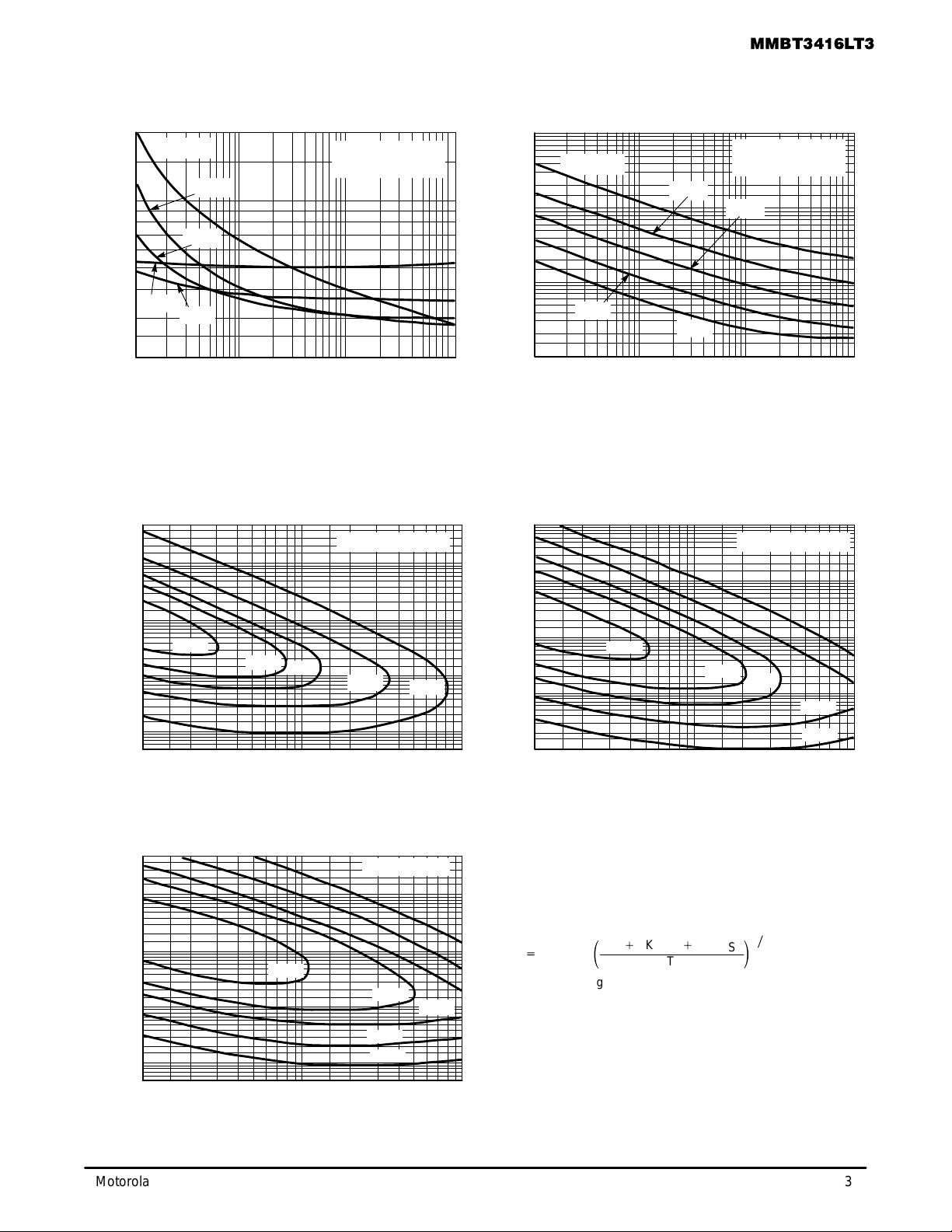
TYPICAL NOISE CHARACTERISTICS
(VCE = 5.0 Vdc, TA = 25°C)
MMBT3416LT3
20
IC = 1.0 mA
10
7.0
5.0
, NOISE VOLTAGE (nV)
n
e
10 µA
3.0
2.0
10 20 50 100 200 500 1 k 2 k 5 k 10 k
300 µA
100 µA
30 µA
f, FREQUENCY (Hz)
BANDWIDTH = 1.0 Hz
RS = 0
Figure 3. Noise V oltage
NOISE FIGURE CONTOURS
(VCE = 5.0 Vdc, TA = 25°C)
500 k
200 k
100 k
50 k
20 k
10 k
5k
2k
1k
500
, SOURCE RESISTANCE (OHMS)
S
R
200
100
50
10
2.0 dB
3.0 dB
4.0 dB
20 30 50 70 100 200 300 500 700 1 k 10 20 30 50 70 100 200 300 500 700 1 k
IC, COLLECTOR CURRENT (µA)
BANDWIDTH = 1.0 Hz
6.0 dB
10 dB
100
BANDWIDTH = 1.0 Hz
RS
100 µA
, NOISE CURRENT (pA)
n
I
50
20
10
5.0
2.0
1.0
0.5
0.2
0.1
IC = 1.0 mA
300 µA
30 µA
10 µA
10 20 50 100 200 500 1 k 2 k 5 k 10 k
f, FREQUENCY (Hz)
Figure 4. Noise Current
1M
500 k
200 k
100 k
50 k
20 k
10 k
5k
2k
1k
, SOURCE RESISTANCE (OHMS)
S
500
R
200
100
1.0 dB
IC, COLLECTOR CURRENT (µA)
BANDWIDTH = 1.0 Hz
2.0 dB
3.0 dB
≈∞
5.0 dB
8.0 dB
Figure 5. Narrow Band, 100 Hz
500 k
200 k
100 k
50 k
20 k
10 k
5k
2k
1k
500
, SOURCE RESISTANCE (OHMS)
S
200
R
100
50
10
1.0 dB
20 30 50 70 100 200 300 500 700 1 k
IC, COLLECTOR CURRENT (µA)
10 Hz to 15.7 kHz
2.0 dB
3.0 dB
5.0 dB
8.0 dB
Figure 7. Wideband
Motorola Small–Signal Transistors, FETs and Diodes Device Data
Figure 6. Narrow Band, 1.0 kHz
Noise Figure is defined as:
2
2
–23
R
S
j/°K)
Ǔ
1ń2
2
e
)
NF+20 log
e
= Noise Voltage of the Transistor referred to the input. (Figure 3)
n
I
= Noise Current of the Transistor referred to the input. (Figure 4)
n
K
= Boltzman’s Constant (1.38 x 10
T
= Temperature of the Source Resistance (°K)
R
= Source Resistance (Ohms)
S
10
ǒ
4KTRS)
n
4KTR
I
n
S
3
Page 4

MMBT3416LT3
TYPICAL STATIC CHARACTERISTICS
, COLLECTOR–EMITTER VOL TAGE (VOLTS)
CE
V
400
200
100
80
FE
h , DC CURRENT GAIN
60
40
0.004
0.006 0.01 0.02 0.03 0.05 0.07 0.1 0.2 0.3 0.5 0.7 1.0
IC, COLLECTOR CURRENT (mA)
TJ = 125°C
25°C
–55°C
2.0
MPS390
VCE = 1.0 V
4
VCE = 10 V
3.0
5.0 7.0 10 20 30 50 70 100
Figure 8. DC Current Gain
1.0
0.8
0.6
0.4
0.2
0
0.002
IC = 1.0 mA 10 mA 100 mA
0.005 0.01 0.02 0.05 0.1 0.2 0.5 1.0 2.0 5.0 10 20 5.0 10 15 20 25 30 35 40
IB, BASE CURRENT (mA)
50 mA
MPS3904
TJ = 25
°
C
100
PULSE WIDTH = 300
DUTY CYCLE
80
60
40
, COLLECTOR CURRENT (mA)
20
C
I
0
0
TA = 25°C
VCE, COLLECTOR–EMITTER VOL TAGE (VOLTS)
≤
2.0%
µ
s
IB = 500 µA
400 µA
300 µA
200 µA
100 µA
1.4
TJ = 25°C
1.2
1.0
0.8
0.6
V, VOLTAGE (VOLTS)
0.4
0.2
0
0.1 0.2 0.5
Figure 9. Collector Saturation Region
V
@ IC/IB = 10
BE(sat)
V
@ VCE = 1.0 V
BE(on)
V
@ IC/IB = 10
CE(sat)
1.0 2.0 5.0 10 20
IC, COLLECTOR CURRENT (mA)
Figure 11. “On” Voltages
50
100
1.6
°θ
0.8
0
–0.8
–1.6
, TEMPERATURE COEFFICIENTS (mV/ C)
V
–2.4
0.1 0.2 0.5
Figure 10. Collector Characteristics
*APPLIES for IC/IB ≤ hFE/2
25°C to 125°C
*
qVC for V
CE(sat)
–55°C to 25°C
25°C to 125°C
q
for V
VB
BE
1.0 2.0 5.0 10 20
IC, COLLECTOR CURRENT (mA)
–55°C to 25°C
Figure 12. T emperature Coefficients
50
100
4
Motorola Small–Signal Transistors, FETs and Diodes Device Data
Page 5

TYPICAL DYNAMIC CHARACTERISTICS
MMBT3416LT3
300
200
100
t, TIME (ns)
500
300
200
70
50
30
20
10
7.0
5.0
3.0
td @ V
3.01.0
2.0 5.0 10
IC, COLLECTOR CURRENT (mA)
Figure 13. Turn–On Time
TJ = 25°C
f = 100 MHz
= 0.5 Vdc
BE(off)
7.0
VCE = 20 V
5.0 V
t
r
VCC = 3.0 V
IC/IB = 10
TJ = 25
20 30 50
°
C
70 100
1000
700
500
300
200
100
t, TIME (ns)
70
50
30
20
10
10
7.0
5.0
3.0
t
s
t
f
VCC = 3.0 V
IC/IB = 10
IB1 = I
B2
TJ = 25
°
C
2.0 5.0 10
3.01.0 7.0
IC, COLLECTOR CURRENT (mA)
Figure 14. T urn–Off Time
C
ib
C
ob
20 30 50
TJ = 25°C
f = 1.0 MHz
70 100
100
70
50
T
f , CURRENT–GAIN BANDWIDTH PRODUCT (MHz)
0.5
0.7 1.0 2.0 3.0 5.0 7.0 10 20 30 50
IC, COLLECTOR CURRENT (mA)
Figure 15. Current–Gain — Bandwidth Product
20
10
Ω
7.0
5.0
3.0
2.0
1.0
, INPUT IMPEDANCE (k )
0.7
ie
h
0.5
0.3
0.2
0.1 0.2 0.5
MPS3904
hfe
≈
200 @ IC = 1.0 mA
2.0 5.0 10
1.0
IC, COLLECTOR CURRENT (mA)
VCE = 10 Vdc
f = 1.0 kHz
TA = 25
°
C
20 50
100
2.0
C, CAPACITANCE (pF)
1.0
0.1 0.2 0.5 1.0 2.0 5.0 10 20 500.05
200
VCE = 10 Vdc
f = 1.0 kHz
100
TA = 25
70
m
50
30
20
10
7.0
5.0
oe
h , OUTPUT ADMITTANCE ( mhos)
3.0
2.0
0.1 0.2 0.5
VR, REVERSE VOLTAGE (VOLTS)
Figure 16. Capacitance
°
C
MPS3904
hfe
≈
200 @ IC = 1.0 mA
2.0 5.0 10
1.0
IC, COLLECTOR CURRENT (mA)
20 50
100
Figure 17. Input Impedance
Motorola Small–Signal Transistors, FETs and Diodes Device Data
Figure 18. Output Admittance
5
Page 6

MMBT3416LT3
1.0
0.7
0.5
D = 0.5
0.3
0.2
0.1
0.07
0.05
(NORMALIZED)
0.03
0.02
r(t) TRANSIENT THERMAL RESIST ANCE
0.01
0.01
4
10
VCC = 30 Vdc
3
10
2
10
1
10
0
10
, COLLECTOR CURRENT (nA)
C
–1
I
10
–2
10
–200 +20 +40 +60 + 80 +100 + 120 + 140 +160
–4
0
0.2
0.1
0.05
0.02
0.01
0.02 0.05 0.1 0.2 0.5 1.0 2.0 5.0 10 20 50 100 200 500 1.0 k 2.0 k 5.0 k 10 k 20 k
SINGLE PULSE
t, TIME (ms)
P
(pk)
FIGURE 19A
t
1
t
2
DUTY CYCLE, D = t1/t
D CURVES APPLY FOR POWER
PULSE TRAIN SHOWN
READ TIME AT t1 (SEE AN–569)
Z
θ
T
J(pk)
JA(t)
•
= r(t)
– TA = P
R
(pk)
θ
JA
Z
Figure 19. Thermal Response
DESIGN NOTE: USE OF THERMAL RESPONSE DATA
A train of periodical power pulses can be represented by the model
as shown in Figure 19A. Using the model and the device thermal
I
CEO
I
I
@ V
CEX
BE(off)
TJ, JUNCTION TEMPERATURE (°C)
CBO
AND
= 3.0 Vdc
response the normalized effective transient thermal resistance of
Figure 19 was calculated for various duty cycles.
To find Z
steady state value R
Example:
The MPS3904 is dissipating 2.0 watts peak under the following
conditions:
t1 = 1.0 ms, t2 = 5.0 ms. (D = 0.2)
Using Figure 19 at a pulse width of 1.0 ms and D = 0.2, the reading of
r(t) is 0.22.
The peak rise in junction temperature is therefore
∆T = r(t) x P
For more information, see AN–569.
, multiply the value obtained from Figure 19 by the
θJA(t)
(pk)
.
θJA
x R
= 0.22 x 2.0 x 200 = 88°C.
θJA
Figure 19A.
θ
2
JA(t)
50 k
100 k
400
200
100
, COLLECTOR CURRENT (mA)
C
I
6.0
4.0
6
60
40
20
10
2.0
100 µs
1.0 ms
10 µs
TC = 25°C
TA = 25°C
dc
TJ = 150°C
CURRENT LIMIT
THERMAL LIMIT
SECOND BREAKDOWN LIMIT
4.0 6.0 8.0 10 20
VCE, COLLECTOR–EMITTER VOL TAGE (VOLTS)
1.0 s
dc
Figure 20.
The safe operating area curves indicate IC–VCE limits of the
transistor that must be observed for reliable operation. Collector load
lines for specific circuits must fall below the limits indicated by the
applicable curve.
40
The data of Figure 20 is based upon T
variable depending upon conditions. Pulse curves are valid for duty
cycles to 10% provided T
the data in Figure 19. At high case or ambient temperatures, thermal
limitations will reduce the power that can be handled to values less
than the limitations imposed by second breakdown.
J(pk)
≤ 150°C. T
= 150°C; TC or TA is
J(pk)
may be calculated from
J(pk)
Motorola Small–Signal Transistors, FETs and Diodes Device Data
Page 7

MMBT3416LT3
INFORMATION FOR USING THE SOT–23 SURFACE MOUNT PACKAGE
MINIMUM RECOMMENDED FOOTPRINT FOR SURFACE MOUNTED APPLICATIONS
Surface mount board layout is a critical portion of the total
design. The footprint for the semiconductor packages must
be the correct size to insure proper solder connection
0.037
0.95
0.035
0.9
SOT–23 POWER DISSIP ATION
The power dissipation of the SOT–23 is a function of the
pad size. This can vary from the minimum pad size for
soldering to a pad size given for maximum power dissipation.
Power dissipation for a surface mount device is determined
by T
die, R
ambient, and the operating temperature, TA. Using the
values provided on the data sheet for the SOT–23 package,
PD can be calculated as follows:
The values for the equation are found in the maximum
ratings table on the data sheet. Substituting these values into
the equation for an ambient temperature TA of 25°C, one can
calculate the power dissipation of the device which in this
case is 225 milliwatts.
The 556°C/W for the SOT–23 package assumes the use
of the recommended footprint on a glass epoxy printed circuit
board to achieve a power dissipation of 225 milliwatts. There
are other alternatives to achieving higher power dissipation
from the SOT–23 package. Another alternative would be to
use a ceramic substrate or an aluminum core board such as
Thermal Clad. Using a board material such as Thermal
Clad, an aluminum core board, the power dissipation can be
doubled using the same footprint.
, the maximum rated junction temperature of the
J(max)
, the thermal resistance from the device junction to
θJA
PD =
T
PD =
150°C – 25°C
556°C/W
J(max)
R
θJA
– T
A
= 225 milliwatts
0.031
0.8
SOT–23
interface between the board and the package. With the
correct pad geometry, the packages will self align when
subjected to a solder reflow process.
0.037
0.95
0.079
2.0
inches
mm
SOLDERING PRECAUTIONS
The melting temperature of solder is higher than the rated
temperature of the device. When the entire device is heated
to a high temperature, failure to complete soldering within a
short time could result in device failure. Therefore, the
following items should always be observed in order to
minimize the thermal stress to which the devices are
subjected.
• Always preheat the device.
• The delta temperature between the preheat and
soldering should be 100°C or less.*
• When preheating and soldering, the temperature of the
leads and the case must not exceed the maximum
temperature ratings as shown on the data sheet. When
using infrared heating with the reflow soldering method,
the difference shall be a maximum of 10°C.
• The soldering temperature and time shall not exceed
260°C for more than 10 seconds.
• When shifting from preheating to soldering, the
maximum temperature gradient shall be 5°C or less.
• After soldering has been completed, the device should
be allowed to cool naturally for at least three minutes.
Gradual cooling should be used as the use of forced
cooling will increase the temperature gradient and result
in latent failure due to mechanical stress.
• Mechanical stress or shock should not be applied during
cooling.
* Soldering a device without preheating can cause excessive
thermal shock and stress which can result in damage to the
device.
Motorola Small–Signal Transistors, FETs and Diodes Device Data
7
Page 8

MMBT3416LT3
P ACKAGE DIMENSIONS
NOTES:
1. DIMENSIONING AND TOLERANCING PER ANSI
Y14.5M, 1982.
2. CONTROLLING DIMENSION: INCH.
A
L
3
1
2
S
B
GV
C
D
H
K
J
CASE 318–08
3. MAXIMUM LEAD THICKNESS INCLUDES LEAD
FINISH THICKNESS. MINIMUM LEAD THICKNESS
IS THE MINIMUM THICKNESS OF BASE
MATERIAL.
INCHES
DIMAMIN MAX MIN MAX
0.1102 0.1197 2.80 3.04
B 0.0472 0.0551 1.20 1.40
C 0.0350 0.0440 0.89 1.11
D 0.0150 0.0200 0.37 0.50
G 0.0701 0.0807 1.78 2.04
H 0.0005 0.0040 0.013 0.100
J 0.0034 0.0070 0.085 0.177
K 0.0140 0.0285 0.35 0.69
L 0.0350 0.0401 0.89 1.02
S 0.0830 0.1039 2.10 2.64
V 0.0177 0.0236 0.45 0.60
STYLE 6:
PIN 1. BASE
MILLIMETERS
2. EMITTER
3. COLLECTOR
ISSUE AF
SOT–23 (TO–236AB)
Motorola reserves the right to make changes without further notice to any products herein. Motorola makes no warranty , representation or guarantee regarding
the suitability of its products for any particular purpose, nor does Motorola assume any liability arising out of the application or use of any product or circuit, and
specifically disclaims any and all liability, including without limitation consequential or incidental damages. “T ypical” parameters which may be provided in Motorola
data sheets and/or specifications can and do vary in different applications and actual performance may vary over time. All operating parameters, including “Typicals”
must be validated for each customer application by customer’s technical experts. Motorola does not convey any license under its patent rights nor the rights of
others. Motorola products are not designed, intended, or authorized for use as components in systems intended for surgical implant into the body, or other
applications intended to support or sustain life, or for any other application in which the failure of the Motorola product could create a situation where personal injury
or death may occur. Should Buyer purchase or use Motorola products for any such unintended or unauthorized application, Buyer shall indemnify and hold Motorola
and its officers, employees, subsidiaries, affiliates, and distributors harmless against all claims, costs, damages, and expenses, and reasonable attorney fees
arising out of, directly or indirectly, any claim of personal injury or death associated with such unintended or unauthorized use, even if such claim alleges that
Motorola was negligent regarding the design or manufacture of the part. Motorola and are registered trademarks of Motorola, Inc. Motorola, Inc. is an Equal
Opportunity/Affirmative Action Employer.
How to reach us:
USA/EUROPE/Locations Not Listed: Motorola Literature Distribution; JAPAN: Nippon Motorola Ltd.: SPD, Strategic Planning Office, 141,
P.O. Box 5405, Denver, Colorado 80217. 1–303–675–2140 or 1–800–441–2447 4–32–1 Nishi–Gotanda, Shagawa–ku, Tokyo, Japan. 03–5487–8488
Customer Focus Center: 1–800–521–6274
Mfax: RMFAX0@email.sps.mot.com – TOUCHTONE 1–602–244–6609 ASIA/PACIFIC: Motorola Semiconductors H.K. Ltd.; 8B Tai Ping Industrial Park,
Moto rola Fa x Back Syst em – US & Canada ONLY 1–800–774–1848 51 Ting Kok Road, Tai Po, N.T., Hong Kong. 852–26629298
HOME PAGE: http://motorola.com/sps/
8
– http://sps.motorola.com/mfax/
◊
Motorola Small–Signal Transistors, FETs and Diodes Device Data
Mfax is a trademark of Motorola, Inc.
MMBT3416L T3/D
 Loading...