

Page 1
MMBT2907A
0.1 20 (3. 04 )
0.11 0( 2.8 0)
0.0 79 (2. 00 )
0.0 70 (1. 80 )
0.0 20( 0. 50)
0.0 13( 0. 35)
0.0 44 (1. 10 )
0.0 35 (0. 90 )
0.0 08 (0. 20 )
0.0 03 (0. 08 )
0.0 04 (0. 1 0)
0.0 00 (0. 0 0)
PNP GENERAL PURPOSE SWITCHING TRANSISTOR
VOLTAGE
60 Volts
POWER
FEATURES
PNP epitaxial silicon, planar design
Collector-emitter voltage VCE = -60V
Collector current IC = -600mA
/HDGIUHHLQFRPSO\ZLWK(85R+6(&GLUHFWLYHV
*UHHQPROGLQJFRPSRXQGDVSHU,(&6WG+DORJHQ)UHH
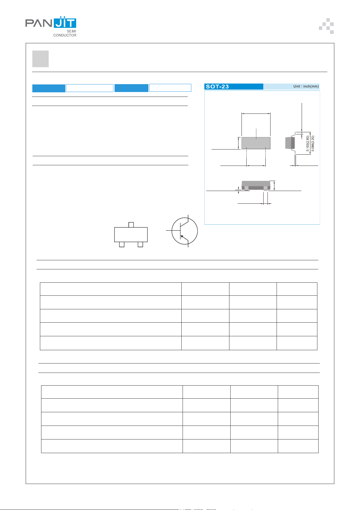
MECHANICAL DATA
Case: SOT-23
Terminals : Solderable per MIL-STD-750,Method 2026
Approx Weight: RXQFHV0.008 grams
Device Marking : M7A
225 mWDWWV
0.0 56( 1. 40)
0.0 47( 1. 20)
0.006( 0.15)M IN.
ABSOLUTE MAXIMUM RATINGS
egatloVrettimE-rotcelloC
egatloVesaB-rotcelloC
egatloVesaB-rettimE
suounitnoC-tnerruCrotcelloC
THERMAL CHATACTERISTICS
Top View
Collector
1
Base
3
2
Emitter
1
BASE
3
COLLECTOR
2
EMITTER
retemaraP lobmyS eulaV stinU
V
ECO
V
OBC
V
OBE
I
C
06- V
06-
0.5-
006- Am
V
V
retemaraP lobmyS
)1etoN(noitapissiDrewoPxaM
erutarepmeTegarotS
eruarepmeTnoitcnuJ
tneibmAotnoitcnuJ,ecnatsiseRlamrehT
Note 1 : Transistor mouted on FR-4 board 70 x 60 x 1mm.
STAD-JUN.29.2005
eulaV stinU
P
OTT
T
GTS
T
J
R
Θ AJ
522 Wm
051ot55-
051ot55-
655
O
O
C
O
C
W/C
PAGE . 1
Page 2

MMBT2907A
ELECTRICAL CHARACTERISTICS (T
retemaraP lobmyS noitidnoCtseT .niM .pyT .xaM stinU
egatloVnwodkaerBrettimE-rotcelloC
egatloVnwodkaerBesaB-rotcelloC
egatloVnwodkaerBesaB-rettimE
tnerruCffotuCesaB
tnerruCffotuCrotcelloC
niaGtnerruCCD
egatloVnoitarutaSrettimE-rotcelloC
egatloVnoitarutaSrettimE-esaB
=25OC, unless otherwise noted)
J
V
OEC
)RB(
V
OBC
)RB(
V
OBE
)RB(
I
LB
I
XEC
I
OBC
h
EF
V
)TAS(EC
V
)TAS(EB
V
V
I
C
I
C
I
C
I
C
I
C
I
C
I
C
I
C
I
C
I
I,Am01-=
C
0= 06- - - V
B
IC01-= µ I,AE0= 06- - - V
IE01-= µ I,AC0= 0.5- - - V
V,V03-=
EC
EC
V
EC
V
EC
T
J
V5.0-= - - 05- An
BE
V,V03-=
V5.0-= - - 05- An
BE
I,V05-=
0= - - 01- An
E
I,V05-=
0=
V,Am1.0-=
V,Am0.1-=
V,Am01-=
521=OC
V,Am051-=
V,Am005-=
I,Am051-=
B
I,Am005-=
B
I,Am051-=
B
I,Am005-=
B
E
V01-=
EC
V01-=
EC
V01-=
EC
V01-=
EC
V01-=
EC
Am51-=
Am05-=
Am51-=
Am05-=
- - 01-
57
001
001
001
05
-
-
-
-
-
-
-
-
-
-
-
-
-
-
-
003
-
4.0-
6.1-
3.1-
6.2-
µA
-
V
V
ecnaticapaCesaB-rotcelloC
ecnaticapaCesaB-rettimE
tcudorPhtdiwdnaB-niaGtnerruC
emiTnO-nruT
emiTyaleD
emiTesiR
emiTffO-nruT
emiTegarotS
emiTllaF
C
OBC
C
OBE
F
T
t
no
t
d
t
r
t
ffo
t
s
t
f
V
VBCI,V2-=
I
C
V
I
C
V
I
C
V
I
C
VCCI,V6-=
VCCI,V6-=
VCCI,V6-=
I,V01-=
BC
C
CC
CC
CC
I
1BI=2B
I
1BI=2B
I
1BI=2B
zHM1=f,0= - - 0.8 Fp
E
zHM1=f,0= - - 03 Fp
V,Am05-=
,V02-=
EC
zHM001=f
V,V03-=
,V5.0-=
EB
I,Am051-=
Am51-=
B
V,V03-=
,V5.0-=
EB
I,Am051-=
Am51-=
B
V,V03-=
,V5.0-=
EB
I,Am051-=
Am51-=
1B
,Am051-=
C
Am51-=
,Am051-=
C
Am51-=
,Am051-=
C
Am51-=
002 - - zHM
- - 54 sn
- - 01 sn
- - 04 sn
- - 001 sn
- - 08 sn
- - 03 sn
STAD-JUN.21.2005
PAGE . 2
Page 3
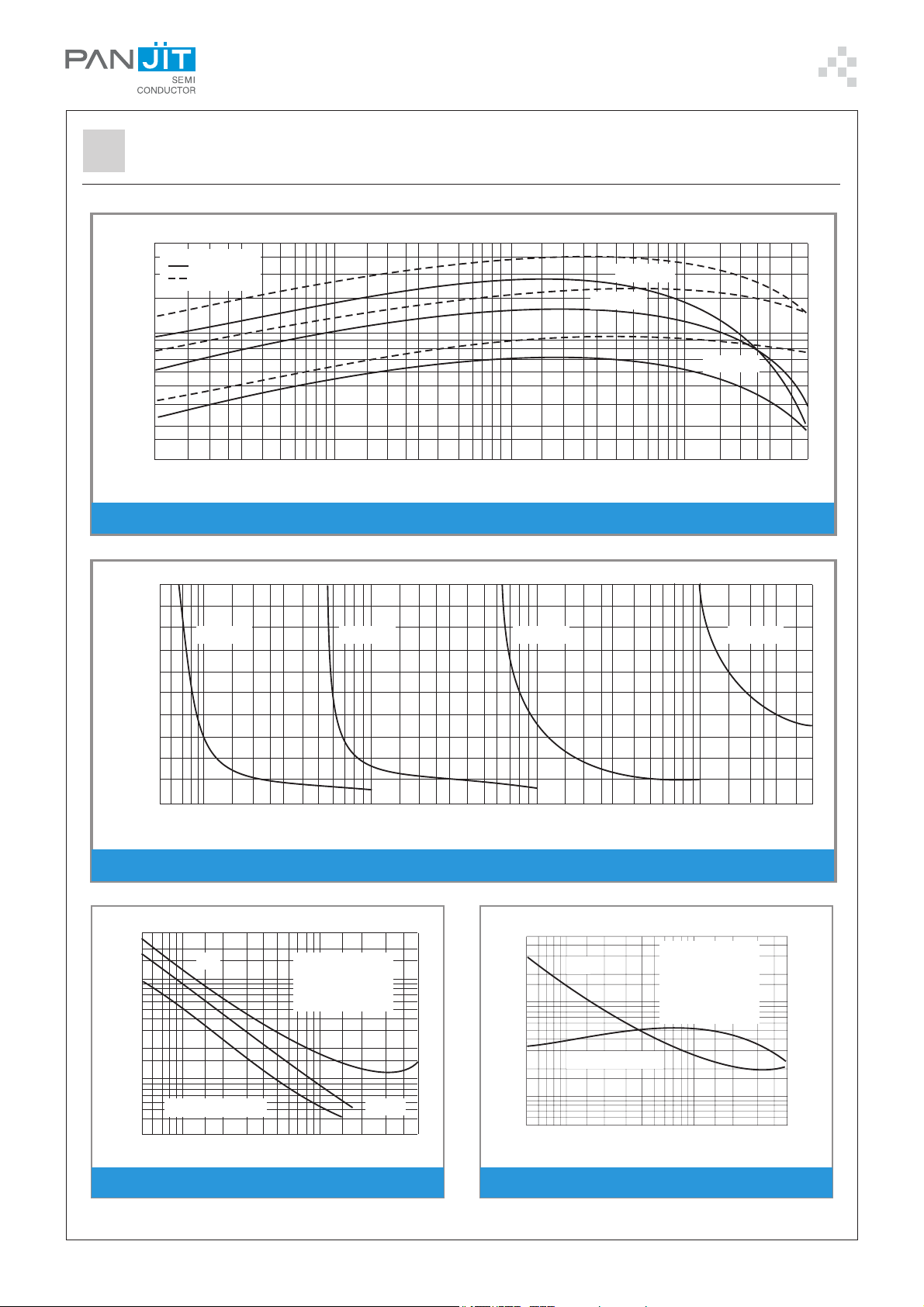
I,COLLECTOR CURRENT (mA)
C
I,COLLECTOR CURRENT
C
I ,COLLECTOR CURRENT (mA)
C
Fig.1-DC Cuttent Gain
Fig.2-Collector Saturation Region
MMBT2907A
3.0
2.0
VCE=-1.0V
VCE=-10V
25 C
1.0
0.7
0.5
0.3
FE
h , NORMALIZED CUTTENT GAIN
0.2
-0.1 -0.2 -0.3 -0.5 -0.7 -1.0 -2.0 -3.0 -5.0 -7.0 -10 -20 -30 -50 -70 -100 -200 -300 -500
I , COLLECTOR CURRENT (mA)
C
Fig.1-DC Cuttent Gain
O
T =125 C
J
O
-55 C
O
-1.0
-0.8
I =-1.0mA
C
-500mA-100mA-10mA
-0.6
-0.4
VOLTAGE (VOLTS)
-0.2
CE
V , COLLECTOR-EMITTER
0
-0.005 -0.01 -0.02 -0.03 -0.07 -0.1 -0.2 -0.7 -1.0 -2.0 -3.0 -5.0 -7.0 -10 -20 -30 -50
-0.05
-0.3 -0.5
I , BASE CUTTENT (mA)
B
Fig.2-Collector Saturation Region
300
200
100
70
t
r
V =-30V
CC
I/I=10
CB
O
T=25 C
J
50
30
20
t, TIME (ns)
10
7.0
5.0
3.0
-5.0 -7.0 -10 -20 -30 -50 -70 -100 -200 -300 -500
td@V =0V
BE(OFF)
I , COLLECTOR CURRENT
C
2.0V
500
300
200
100
t
f
V =-30V
CC
I/I=10
CB
II
B1= B2
O
T=25 C
J
70
50
30
t, TIME (ns)
20
,
t =t -1/8t
ss f
10
7.0
5.0
-5.0 -7.0 -10 -20 -30 -50-70 -100 -200-300 -500
I ,COLLECTOR CURRENT (mA)
C
Fig.3-Turn-On Time Fig.4-Turn-Off Time
STAD-JUN.29.2005
PAGE . 3
Page 4

NF,
NOISE
FIGURE
(dB)
NF,
NOISE
FIGURE
(dB)
R,SOURGE RESISTANCE (OHMS)
S
I ,COLLECTOR CURRENT (mA)
C
I ,COLLECTOR CUTTENT (mA)
C
Fig.5-Frequency Effects
Fig.6-Source Resistance Effects
Fig.8-Current-Gain-Bandwidth Product
Fig.9-On Voltage
Fig.10-Temperature Coefficients
MMBT2907A
10
8.0
I =-1.0mA,R =430
CS
-500 A,R =560
6.0
4.0
2.0
NF, NOISE FIGURE (dB)
0
0.01 0.02 0.05 0.1 0.2 0.5 1.0 2.0 5.0 10 20 50 100
R =OPTIMUM SOURCE RESISANCE
S
mW
-50 A,R =2.7k
mW
-100 A,R =1.6
mW
W
S
f,FREQUENCY (kHz)
Fig.5-Frequency Effects
30
C
20
eb
10
7.0
5.0
C,CAPACITANCE (pF)
3.0
2.0
-0.1 -0.2 -0.3 -0.5 -1.0 -2.0-3.0 -5.0 -10 -20 -30
REVERSE VOLTAGE (VOLTS)
Fig.7-Capacitances
C
cb
10
f=1.0kHz
8.0
I =-50 A
m
C
-100 A
6.0
m
-500 A
m
-1.0mA
4.0
NF, NOISE FIGURE (dB)
2.0
0
50 100 200 500 1.0k 2.0k 5.0k 10k 20k 50k
R , SOURGE RESISTANCE (OHMS)
S
Fig.6-Source Resistance Effects
400
300
200
100
80
60
PRODUCT (MHz)
40
V =-20V
CE
O
T=25 C
J
30
T
f , CURRENT-GAIN-BANDWIDTH
20
-1.0 -2.0 -5.0 -10 -20 -50 -100 -200 -500-1000
I , COLLECTOR CUTTENT (mA)
C
Fig.8-Current-Gain-Bandwidth Product
-1.0
-0.8
-0.6
-0.4
V,VOLTAGE (VOLTS)
-0.2
0
-0.1 -0.2 -0.5 -1.0 -2.0 -5.0 -10 -20 -50 -100-200 -500
STAD-JUN.29.2005
O
T=25 C
J
V@
V@I/I=10
BE(sat) C B
I/I=10
CE(sat)
CB
I ,COLLECTOR CURRENT (mA)
C
Fig.9-On Voltage
V @V =-10V
BE(on) CE
+0.5
0
RforV
QVC CE(sat)
-0.5
O
-1.0
-1.5
-2.0
COEFFICIENT (mV/ C)
-2.5
-0.1 -0.2 -0.5 -1.0 -2.0 -5.0-10 -20 -50 -100 -200 -500
I ,COLLECTOR CUTTENT (mA)
C
RforV
QVB BE
Fig.10-Temperature Coefficients
PAGE . 4
Page 5

MMBT2907A
MOUNTING PAD LAYOUT
SOT-23
0.035 MIN.
(0.90) MIN.
0.043
(1.10)
0.106
(2.70)
0.031 MIN.
(0.80) MIN.
0.037
(0.95)
Unit inch(mm):
0.043
(1.10)
0.078
(2.00)
ORDER INFORMATION
• Packing information
T/R - 12K per 13" plastic Reel
T/R - 3K per 7” plastic Reel
STAD-JUN.29.2005
PAGE . 5
Page 6

MMBT2907A
Part No_packing code_Version
00%7$_R1_00001
MMBT2907A_R2_00001
For example :
RB500V-40_R2_00001
Serial number
Part No.
Version code means HF
Packing size code means 13"
Packing type means T/R
Packing type 1st Code Packing size code 2nd Code HF or RoHS 1st Code 2nd~5
Tape and Ammunition Box
(T/B)
Tape and Reel
(T/R)
Bulk Packing
(B/P)
Tube Packing
(T/P)
Tape and Reel (Right Oriented)
(TRR)
Tape and Reel (Left Oriented)
(TRL)
FORMING F
Packing Code XX Version Code XXXXX
th
Code
A N/A 0 HF 0 serial number
R 7" 1 RoHS 1 serial number
B 13" 2
T 26mm X
S 52mm Y
PANASERT T/B CATHODE UP
L
PANASERT T/B CATHODE DOWN
(PBCU)
(PBCD)
U
D
STAD-JUN.29.2005
PAGE . 6
Page 7

MMBT2907A
Disclaimer
z Reproducing and modifying information of the document is prohibited without
permission from Panjit International Inc..
z Panjit International Inc. reserves the rights to make changes of the content herein the
document anytime without notification. Please refer to our website for the latest
document.
z Panjit International Inc. disclaims any and all liability arising out of the application or
use of any product including damages incidentally and consequentially occurred.
z Panjit International Inc. does not assume any and all implied warranties, including
warranties of fitness for particular purpose, non-infringement and merchantability.
z Applications shown on the herein document are examples of standard use and
operation. Customers are responsible in comprehending the suitable use in particular
applications. Panjit International Inc. makes no representation or warranty that such
applications will be suitable for the specified use without further testing or modification.
z The products shown herein are not designed and authorized for equipments requiring
high level of reliability or relating to human life and for any applications concerning
life-saving or life-sustaining, such as medical instruments, transportation equipment,
aerospace machinery et cetera. Customers using or selling these products for use in
such applications do so at their own risk and agree to fully indemnify Panjit
International Inc. for any damages resulting from such improper use or sale.
STAD-JUN.29.2005
PAGE . 7
 Loading...