

Page 1
October 1987
Revised January 1999
MM74C150 • MM82C19 16-Line to 1-Line Multiplexer 3-STATE • 16-Line to 1-Line Multiplexer
© 1999 Fairchild Semiconductor Corporation DS005891.prf www.fairchildsemi.com
MM74C150 • MM82C19
16-Line to 1-Line Multiplexer 3-STATE •
16-Line to 1-Line Multiplexer
General Description
The MM74C150 and M M8 2C19 multiplex 16 digital line s to
1 output. A 4-bit ad dre ss code determines th e p articular 1of-16 inputs which is routed to the output. The data is
inverted from input to output.
A strobe override places t he output of MM74C150 in the
logical “1” state and the output of MM82C19 in the highimpedance state.
All inputs are protected from damage due to static discharge by diode clamps to V
CC
and GND.
Features
■ Wide supply voltage range: 3.0V to 15V
■ Guaranteed noise margin: 1.0V
■ High noise immunity: 0.45 V
CC
(typ.)
■ TTL compatibility: Drive 1 TTL Load
Ordering Code:
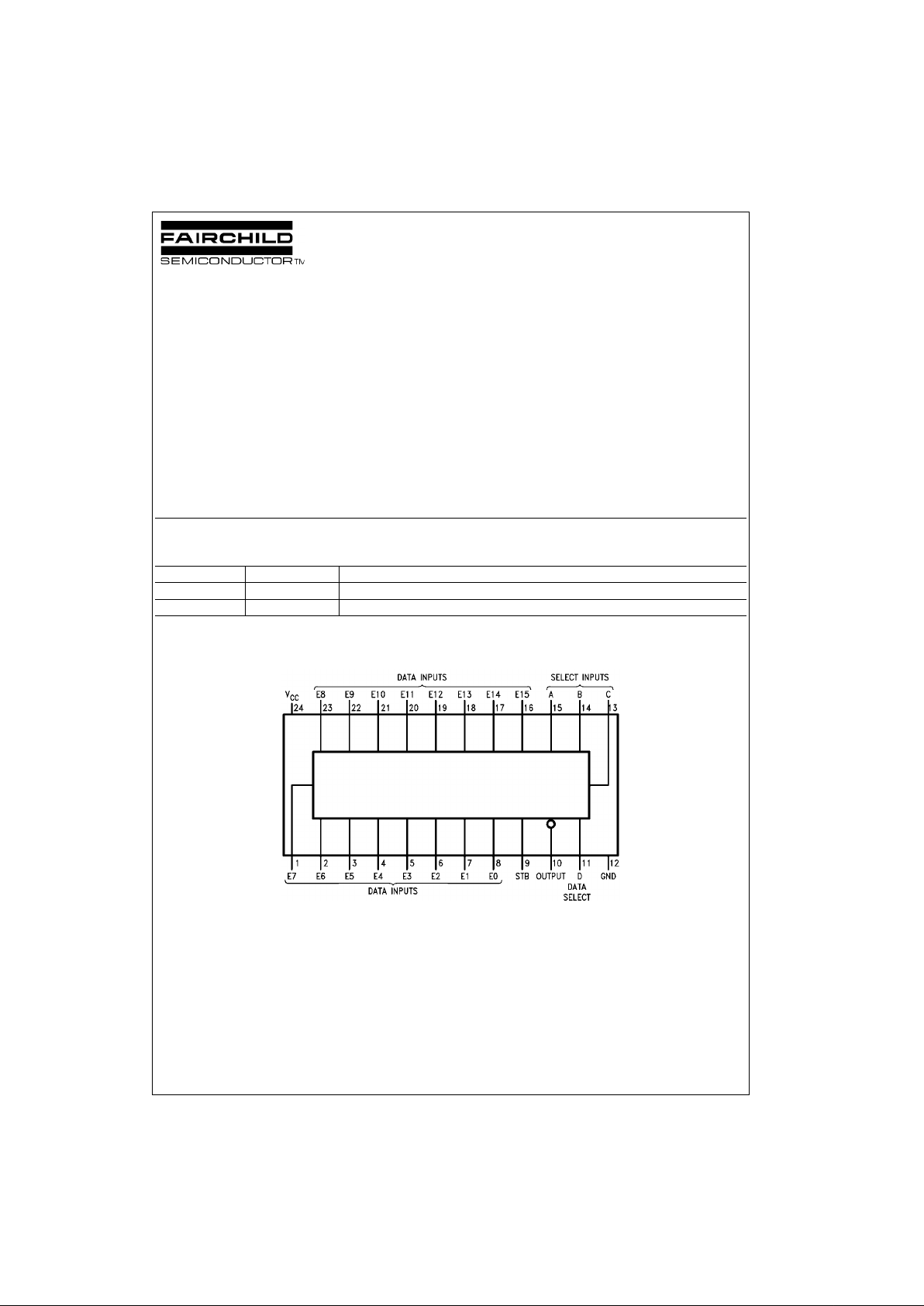
Connection Diagram
Pin Assignments for DIP
Order Number Package Number Package Description
MM74C150N N24A 24-Lead plastic Dual-In-Line Package (PDIP), JEDEC MS-010, 0.600” Wide
MM82C19N N24A 24-Lead plastic Dual-In-Line Package (PDIP), JEDEC MS-010, 0.600” Wide
Page 2
www.fairchildsemi.com 2
MM74C150 • MM82C19
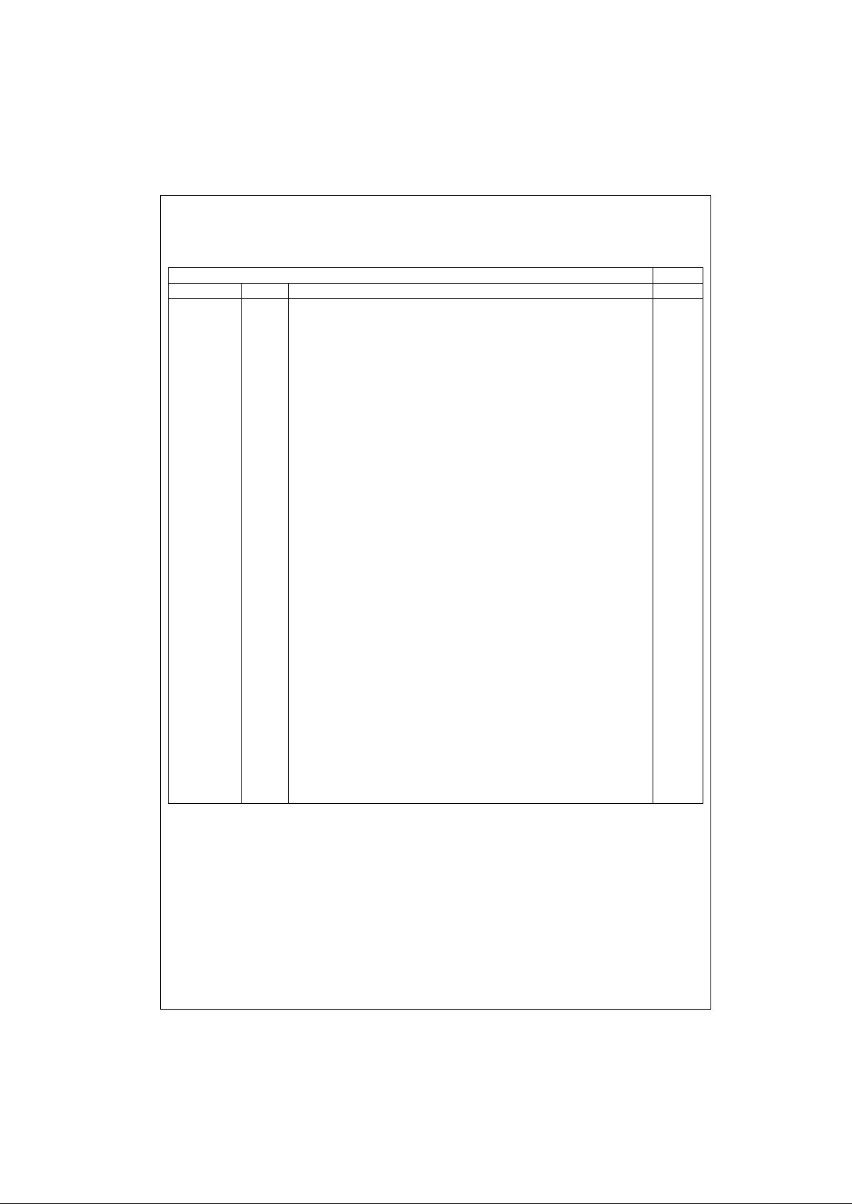
Truth Table
MM74C150
Note 1: For MM72C19/MM82C19 this would be Hi-Z, ever ything else is the same.
Inputs Output
D C B A STROBE E0 E1 E2 E3 E4 E5 E6 E7 E8 E9 E10 E11 E12 E13 E14 E15 W
XXXX 1 XXXXXXXXXXXX XXX X1 (Note 1)
0000 0 0XXXXXXXXXX XXXX X 1
0000 0 1XXXXXXXXXX XXXX X 0
0001 0 X0XXXXX XXXX XXXX X 1
0001 0 X1XXXXX XXXX XXXX X 0
0010 0 XX0XXXX XXXX XXXX X 1
0010 0 XX1XXXX XXXX XXXX X 0
0011 0 XXX0XXX XXXX XXXX X 1
0011 0 XXX1XXX XXXX XXXX X 0
0100 0 XXXX0XX XXXX XXXX X 1
0100 0 XXXX1XX XXXX XXXX X 0
0101 0 XXXXX0X XXXX XXXX X 1
0101 0 XXXXX1X XXXX XXXX X 0
0110 0 XXXXXX0 XXXX XXXX X 1
0110 0 XXXXXX1 XXXX XXXX X 0
0111 0 XXXXXXX0 XXX XXXX X 1
0111 0 XXXXXXX1 XXX XXXX X 0
1000 0 XXXXXXX X0XX XXXX X 1
1000 0 XXXXXXX X1XX XXXX X 0
1001 0 XXXXXXX XX0X XXXX X 1
1001 0 XXXXXXX XX1X XXXX X 0
1010 0 XXXXXXX XXX 0 XXXX X 1
1010 0 XXXXXXX XXX 1 XXXX X 0
1011 0 XXXXXXX XXXX 0 XXX X 1
1011 0 XXXXXXX XXXX 1 XXX X 0
1100 0 XXXXXXX XXXX X0 XX X 1
1100 0 XXXXXXX XXXX X1 XX X 0
1101 0 XXXXXXX XXXX XX 0X X 1
1101 0 XXXXXXX XXXX XX 1X X 0
1110 0 XXXXXXX XXXX XXX 0 X 1
1110 0 XXXXXXX XXXX XXX 1 X 0
1111 0 XXXXXXX XXXX XXXX 0 1
1111 0 XXXXXXX XXXX XXXX 1 0
Page 3
3 www.fairchildsemi.com
MM74C150 • MM82C19
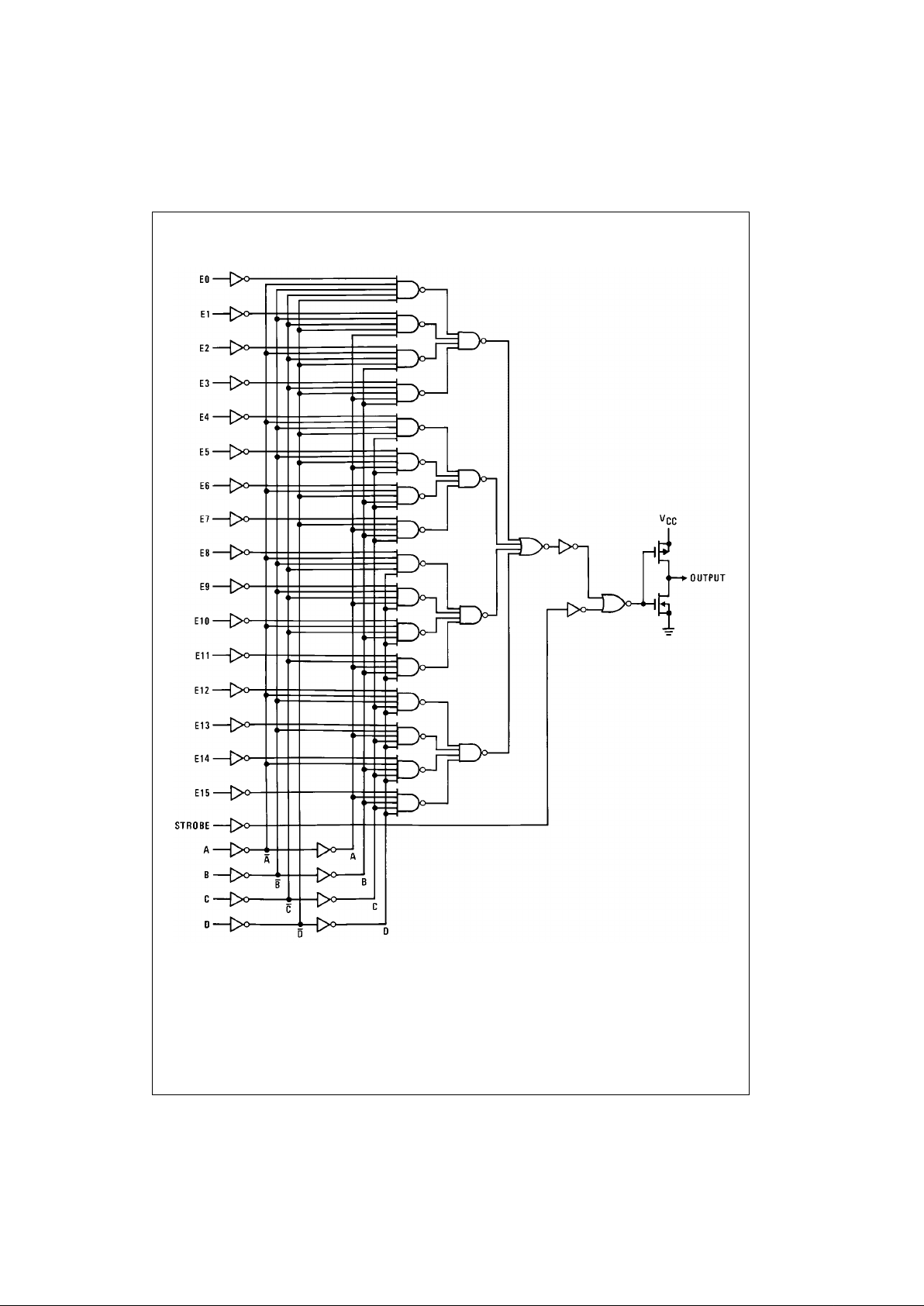
Logic Diagrams
MM74C150
Page 4

www.fairchildsemi.com 4
MM74C150 • MM82C19
Logic Diagrams (Continued)
MM82C19
Page 5

5 www.fairchildsemi.com
MM74C150 • MM82C19
Absolute Maximum Ratings(Note 2)
Note 2: “Absolute Maximum Rat ings” are tho se values beyond which the
safety of the device cannot be guaranteed. Ex c ept for “ Operating Temperature Range” they are not mea nt to imply that the devices sh ould be operated at these limits. The Elec trical Cha racteristic table provides condit ions
for actual device operation.
DC Electrical Characteristics
Min/Max limits apply across temperature range unless otherwise noted.
Voltage at Any Pin −0.3V to VCC+0.3V
Operating Temperature Range −40°C to +85°C
Storage Temperature Range −65°C to +150°C
Power Dissipation
Dual-In-Line 700 mW
Small Outline 500 mW
Operating V
CC
Range 3.0V to 15V
V
CC
18V
Lead Temperature
(soldering, 10 seconds) 260°C
Symbol Parameter Conditions Min Typ Max Units
CMOS to CMOS
V
IN(1)
Logical “1” Input Voltage VCC = 5.0V 3.5 V
VCC = 10V 8.0 V
V
IN(0)
Logical “0” Input Voltage VCC = 5.0V 1.5 V
VCC = 10V 2.0 V
V
OUT(1)
Logical “1” Output Voltage VCC = 5.0V, IO = −10 µA4.5 V
VCC = 10V, IO = −10 µA9.0 V
V
OUT(0)
Logical “0” Output Voltage VCC = 5.0V, IO = +10 µA0.5V
VCC = 10V, IO = +10 µA1.0V
I
IN(1)
Logical “1” Input Current VCC = 15V, VIN = 15V 0.005 1.0 V
I
IN(0)
Logical “0” Input Current VCC = 15V, VIN = 0V −1.0 −0.005 µA
I
OZ
Output Current in High
Impedance State
MM82C19 VCC = 15V, VO = 15V 0.005 1.0 µA
VCC = 15V, VO = 0V −1.0 −0.005 µA
I
CC
Supply Current VCC = 15V 0.05 300 µA
CMOS/LPTTL Interface
V
IN(1)
Logical “1” Input Voltage 74C, 82C, VCC = 4.75V VCC−1.5 V
V
IN(0)
Logical “0” Input Voltage 74C, 82C, VCC = 4.75V 0.8 V
V
OUT(1)
Logical “1” Output Voltage 74C, 82C, VCC = 4.75V, IO = −1.6 mA 2.4 V
V
OUT(0)
Logical “0” Output Voltage 74C, 82C, VCC = 4.75V, IO = 1.6 mA 0.4 V
Output Drive (Short Circuit Current)
I
SOURCE
Output Source Current VCC = 5.0V, V
OUT
= 0V, TA = 25°C −4.35 −8mA
(P-Channel)
I
SOURCE
Output Source Current VCC = 10V, V
OUT
= 0V, TA = 25°C −20 −40 mA
(P-Channel)
I
SINK
Output Sink Current VCC = 5.0V, V
OUT
= VCC, TA = 25°C4.35 8 mA
(N-Channel)
I
SINK
Output Sink Current VCC = 10V, V
OUT
= VCC, TA = 25°C2040 mA
(N-Channel)
Page 6

www.fairchildsemi.com 6
MM74C150 • MM82C19
AC Electrical Charac teristics (Note 3)
T
A
= 25°C, CL = 50 pF, unless otherwise noted
Note 3: AC Parameters are guara nt eed by DC correlated testin g.
Note 4: Capacitance is guaranteed by periodic testing.
Note 5: C
PD
determines th e no load AC power con sumption o f any CMOS device. For comp lete explanatio n, see Family Character istics, appli cation not e
AN-90.
Symbol Parameter Conditions Min Typ Max Units
t
pd0
, t
pd1
Propagation Delay Time to a VCC = 5.0V 250 600 ns
Logical “0” or Logical “1” VCC = 10V 110 300 ns
from Data Inputs to Output VCC = 5.0V, CL = 150 pF 290 650 ns
VCC = 10V, CL = 150 pF 120 330 ns
t
pd0
, t
pd1
Propagation Delay Time to a VCC = 5.0V 290 650 ns
Logical “0” or Logical “1” VCC = 10V 120 330 ns
from Data Select Inputs to
Output
t
pd0
, t
pd1
Propagation Delay Time to a VCC = 5.0V 120 300 ns
Logical “0” or Logical “1” VCC = 10V 55 150 ns
from Strobe to Output
MM74C150
t1H, t
0H
Delay from Strobe to High VCC = 5.0V, RL = 10k, CL = 5 pF 80 200 ns
Impedance State VCC = 10V, RL = 10k, CL = 5 pF 60 150 ns
MM82C19
tH1, t
H0
Delay from Strobe to Logical VCC = 5.0V, RL = 10k, CL = 5 pF 80 250 ns
“1” Level or to Logical “0” VCC = 10V, RL = 10k, CL = 5 pF 30 120 ns
Level (from High Impedance State)
MM82C19
C
IN
Input Capacitance Any Input (Note 4) 5.0 pF
C
OUT
Output Capacitance (Note 4) 11.0 pF
MM82C19
C
PD
Power Dissipation Capacitance (Note 5) 100 pF
Page 7

7 www.fairchildsemi.com
MM74C150 • MM82C19
Switching Time Waveforms
CMOS to CMOS
t
1H
and t
H1
t
1H
t
H1
t0H and t
H0
t
0H
Note: Delays measured with input tr, tf ≤ 20 ns.
t
H0
Page 8

Fairchild does not assume any responsibility for use of any circuitry described, no circuit patent licenses are implied and Fairchild reserves the right at any time without notice to change said circuitry and specifications.
MM74C150 • MM82C19 16-Line to 1-Line Multiplexer 3-STATE • 16-Line to 1-Line Multiplexer
LIFE SUPPORT POLICY
FAIRCHILD’S PRODUCTS ARE NOT AUTHORIZED FOR USE AS CRITICAL COMPONENTS IN LIFE SUPPORT
DEVICES OR SYSTEMS WITHOUT THE EXPRESS WRITTEN APPROVAL OF THE PRESIDENT OF FAIRCHILD
SEMICONDUCTOR CORPORATION. As used herein:
1. Life support devices or systems are devices or syste ms
which, (a) are intended for surgical implant into the
body, or (b) support or sustain life, and (c) whose failure
to perform when properly used in accordance with
instructions for use provided in the labeling, can be reasonably expected to result in a significant injury to the
user.
2. A criti cal comp onent in any comp onent of a life suppor t
device or system whose failure to perform can be reasonably expected to cause the failure of the life suppor t
device or system, or to affect its safety or effectiveness.
www.fairchildsemi.com
Physical Dimensions inches (millimeters) unless otherwise noted
24-Lead Plastic Dual-In-Line Package (PDIP), JEDEC MS-010, 0.600” Wide
Package Number N24A
 Loading...