

Page 1
October 1987
Revised January 1999
MM80C95 • MM80C97 • MM80C98 3-STATE Hex Buffers • 3-STATE Hex Inverters
© 1999 Fairchild Semiconductor Corporation DS005907.prf www.fairchildsemi.com
MM80C95 • MM80C97 • MM80C98
3-STATE Hex Buffers • 3-STATE Hex Inverters
General Description
The MM80C95, MM80C97 and MM80C98 gates are monolithic complementary MOS (CMOS) integrated circu i ts co nstructed with N- and P-channel enhancement mode
transistors. The MM80C95 and the MM80C97 convert
CMOS or TTL outputs to 3-S TATE outputs with no logic
inversion, the MM80C98 provides the logical op posite of
the input signal. The MM80C95 has common 3-STATE
controls for all six devices. The MM80C97 and the
MM80C98 have two 3-STATE controls ; one for two devices
and one for the other four d evices. Inputs are pro tected
from damage due to static discharge by diode clam ps to
V
CC
and GND.
Features
■ Wide supply voltage range: 3.0V to 15V
■ Guaranteed noise margin: 1.0V
■ High noise immunity: 0.45 V
CC
(typ.)
■ TTL compatible: Drive 1 TTL Load
Applications
• Bus drivers: Typical propagation delay into 150 pF load
is 40 ns
Ordering Code:
Devices also available in Tape and Reel. Specify by appending the suffix letter “X” to the ordering code.
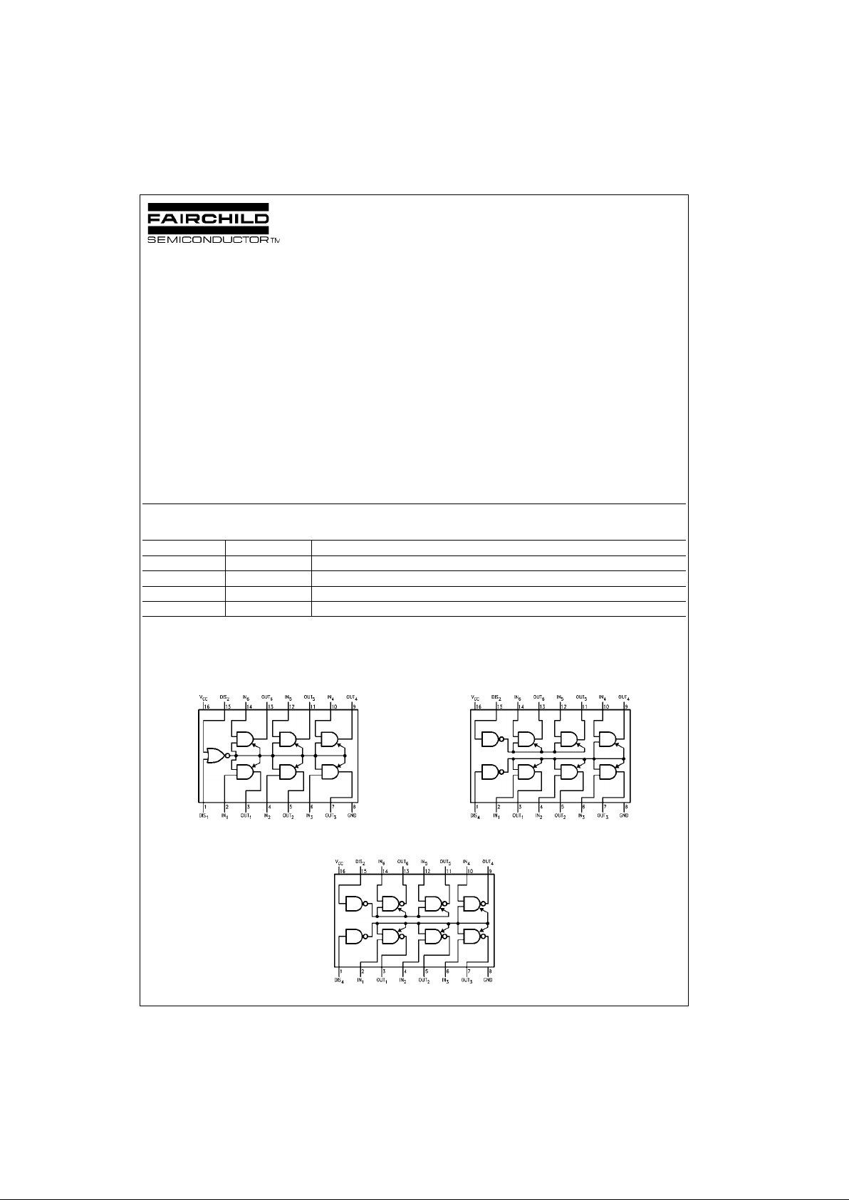
Connection Diagrams
Pin Assignments for DIP
MM80C95
Top View
MM80C97
Top V iew
MM80C98
Top View
Order Number Package Number Package Description
MM80C95N N16E 16-Lead Plastic Dual-In-Line Package (PDIP), JEDEC MS-001, 0.300” Wide
MM80C97M M16A 16-Lead Small Outline Integrated Circuit (SOIC), JEDEC MS-012, 0.150” Narrow
MM80C97N N16E 16-Lead Plastic Dual-In-Line Package (PDIP), JEDEC MS-001, 0.300” Wide
MM80C98N N16E 16-Lead Plastic Dual-In-Line Package (PDIP), JEDEC MS-001, 0.300” Wide
Page 2
www.fairchildsemi.com 2
MM80C95 • MM80C97 • MM80C98
Schematic Diagrams
MM80C95 3-STATE
MM80C97 3-STATE
MM80C98 3-STATE
Truth Tables
MM80C95
MM80C97
MM80C98
X = Irrelevant
Note 1: Output 5–6 only
Note 2: Output 1–4 only
Disable Input Input Output
DIS
1
DIS
2
0000
0011
01XH-z
10XH-z
11XH-z
Disable Input Input Output
DIS
4
DIS
2
0000
0011
X 1 X H-z ( Note 1)
1 X X H-z (Note 2)
Disable Input Input Output
DIS
4
DIS
2
0001
0010
X 1 X H-z ( Note 1)
1 X X H-z (Note 2)
Page 3
3 www.fairchildsemi.com
MM80C95 • MM80C97 • MM80C98
Absolute Maximum Ratings(Note 3)
Note 3: “Absolute Maximum Rat ings” are tho se values beyond which the
safety of the device cannot be guaranteed. Ex c ept for “ Operating Temperature Range” they are not me ant to imply that the device should be operated
at these limits. The table of “E lectr ical Cha racter istics” p rovides condition s
for actual device operation.
DC Electrical Characteristics
Min/Max limits apply across temperature range unless otherwise noted
Voltage at Any Pin −0.3V to VCC + 0.3V
Operating Temperature Range −40°C to +85°C
Storage Temperature Range −65°C to +150°C
Power Dissipation (P
D
)
Dual-In-Line 700 mW
Small Outline 500 mW
Power Supply Voltage (V
CC
)18V
Lead Temperature
(Soldering, 10 seconds) 260°C
Symbol Parameter Conditions Min Typ Max Units
CMOS TO CMOS
V
IN(1)
Logical “1” Input Voltage VCC = 5V 3.5 V
VCC = 10V 8.0 V
V
IN(0)
Logical “0” Input Voltage VCC = 5V 1.5 V
VCC = 10V 2.0 V
V
OUT(1)
Logical “1” Output Voltage VCC = 5V 4.5 V
VCC = 10V 9.0 V
V
OUT(0)
Logical “0” Output Voltage VCC = 5V 0.5 V
VCC = 10V 1.0 V
I
IN(1)
Logical “1” Input Current VCC = 15V 0.005 1.0 µA
I
IN(0)
Logical “0” Input Current −1.0 −0.005 µA
I
OZ
Output Current in High VCC = 15V, VO = 15V 0.005 1.0 µA
Impedance State VCC = 15V, VO = 0V −1.0 −0.005 µA
I
CC
Supply Current VCC = 15V 0.01 15 µA
TTL INTERFACE
V
IN(1)
Logical “1” Input Voltage VCC = 4.75V VCC − 1.5 V
V
IN(0)
Logical “0” Input Voltage VCC = 4.75V 0.8 V
V
OUT(1)
Logical “1” Output Voltage VCC = 4.75V, 2.4 V
IO = −1.6 mA
V
OUT(0)
Logical “0” Output Voltage VCC = 4.75V, 0.4 V
IO = 1.6 mA
OUTPUT DRIVE (Short Circuit Current)
I
SOURCE
Output Source Current VCC = 5V, V
IN(1)
= 5V −4.35 mA
TA = 25°C, V
OUT
= 0V
I
SOURCE
Output Source Current VCC = 10V, V
IN(1)
= 10V −20 mA
TA = 25°C, V
OUT
= 0V
I
SINK
Output Sink Current VCC = 5V, V
IN(0)
= 0V 4.35 mA
TA = 25°C, V
OUT
= V
CC
I
SINK
Output Sink Current VCC = 10V, V
IN(0)
= 0V 20 mA
TA = 25°C, V
OUT
= V
CC
Page 4

www.fairchildsemi.com 4
MM80C95 • MM80C97 • MM80C98
AC Electrical Charac teristics (Note 4)
TA = 25°C, CL = 50 pF, unless otherwise noted.
Note 4: AC Parameters are guara nt eed by DC correlated testing.
Note 5: Capacitance is guaranteed by periodic testing.
Note 6: C
PD
determines the no load AC power consumption of any C M OS device. For complete explanation se e Family Characteristics applic ation note
AN-90.
AC Test Circuits and Switchi ng Time Waveforms
t
pd0, tpd1
CMOS to CMOS
t
1H
and t
H1
t
1H
Symbol Parameter Conditions Min Typ Max Units
t
pd0
, t
pd1
Propagation Delay Time to a Logical “0” or
Logical “1” from Data Input to Output
MM80C95, MM80C97 VCC = 5V 60 100 ns
VCC = 10V 25 40 ns
MM80C98 VCC = 5V 70 150 ns
VCC = 10V 35 75 ns
t
pd0
, t
pd1
Propagation Delay Time to a Logical “0” or
Logical “1” from Data Input to Output
MM80C95, MM80C97 VCC = 5V, CL = 150 pF 85 160 ns
VCC = 10V, CL = 150 pF 40 80 ns
MM80C98 VCC = 5V, CL = 150 pF 95 210 ns
VCC = 10V, CL = 150 pF 45 110 ns
t1H, t
0H
Delay from Disable Input to High Impedance RL = 10k, CL = 5 pF
State, (from Logical “1” or Logical “0”)
MM80C95 VCC = 5V 80 135 ns
VCC = 10V 50 90 ns
MM80C97 VCC = 5V 70 125 ns
VCC = 10V 50 90 ns
MM80C98 VCC = 5V 90 170 ns
VCC = 10V 70 125 ns
tH1, t
H0
Delay from Disable Input to Logical “1” Level RL = 10k, CL = 50 pF
(from High Impedance State)
MM80C95 VCC = 5V 120 200 ns
VCC = 10V 50 90 ns
MM80C96 VCC = 5V 130 225 ns
VCC = 10V 60 110 ns
MM80C98 VCC = 5V 120 200 ns
VCC = 10V 50 90 ns
C
IN
Input Capacitance Any Input (Note 5) 5.0 pF
C
OUT
Output Capacitance 3-STATE Any Output (Note 5) 11 pF
C
PD
Power Dissipation Capacitance (Note 6) 60 pF
Page 5

5 www.fairchildsemi.com
MM80C95 • MM80C97 • MM80C98
AC Test Circuits and Switching Time Waveforms (Continued)
t
H1
t0H and t
H0
t
0H
t
H0
Note: Delays measured with input tr, tf ≤ 20 ns.
Typical Performance Characteristics
Propagation Delay vs Load Capacitance ∆t
pd
/pF vs Power Supply Voltage
N-Channel Output Drive at 25°C P-Channel Output Drive at 25°C
Page 6

www.fairchildsemi.com 6
MM80C95 • MM80C97 • MM80C98
Physical Dimensions inches (millimeters) unless otherwise noted
16-Lead Small Outline Integrated Circuit (SOIC), JEDEC MS-012, 0.150” Narrow
Package Number M16A
Page 7

Fairchild does not assume any responsibility for use of any circuitry described, no circuit patent licenses are implied and Fairchild reserves the ri ght at any time without notice to change said circuitry and specifications.
MM80C95 • MM80C97 • MM80C98 3-STATE Hex Buffers • 3-STATE Hex Inverters
LIFE SUPPORT POLICY
FAIRCHILD’S PRODUCTS ARE NOT AUTHORIZED FOR USE AS CRITICAL COMPONENTS IN LIFE SUPPORT
DEVICES OR SYSTEMS WITHOUT THE EXPRESS WRITTEN APPROVAL OF THE PRESIDENT OF FAIRCHILD
SEMICONDUCTOR CORPORATION. As used herein:
1. Life support devices or systems are devices or syste ms
which, (a) are intended for surgical implant into the
body, or (b) support or sustain life, and (c) whose failure
to perform when properly used in accordance with
instructions for use provided in the labeling, can be reasonably expected to result in a significant injur y to the
user.
2. A critical component in a ny compon ent of a life suppo r t
device or system whose failure to p erform can be r easonably expected to cause the failure of the life suppor t
device or system, or to affect its safety or effectiveness.
www.fairchildsemi.com
Physical Dimensions inches (millimeters) unless otherwise noted (Continued)
16-Lead Plastic Dual-In-Line Package (PDIP), JEDEC MS-001, 0.300” Wide
Package Number N16E
 Loading...