

Page 1
查询MM70C95供应商
MM70C95/MM80C95, MM70C97/MM80C97
TRI-STATE
MM70C96/MM80C96, MM70C98/MM80C98
TRI-STATE Hex Inverters
Hex Buffers
É
February 1988
MM70C95/MM80C95, MM70C97/MM80C97 TRI-STATE Hex Buffers
MM70C96/MM80C96, MM70C98/MM80C98 TRI-STATE Hex Inverters
General Description
These gates are monolithic complementary MOS (CMOS)
integrated circuits constructed with N- and P-channel enhancement mode transistors. The MM70C95/MM80C95
and the MM70C97/MM80C97 convert CMOS or TTL outputs to TRI-STATE outputs with no logic inversion, the
MM70C96/MM80C96 and the MM70C98/MM80C98 provide the logical opposite of the input signal. The MM70C95/
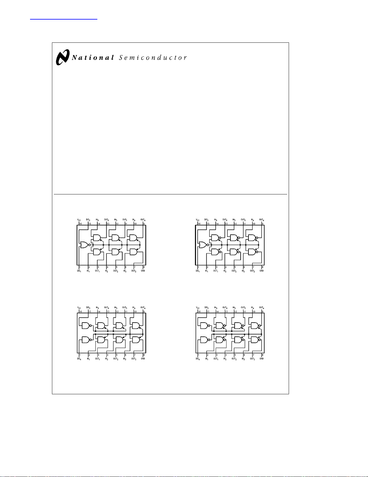
MM80C95 and the MM70C96/MM80C96 have common
TRI-STATE controls for all six devices. The MM70C97/
MM80C97 and the MM70C98/MM80C98 have two TRISTATE controls; one for two devices and one for the other
four devices. Inputs are protected from damage due to static discharge by diode clamps to V
and GND.
CC
Connection Diagrams (Dual-In-Line Packages)
MM70C95/MM80C95
Top View
Order Number MM70C95 or MM80C95
TL/F/5907– 1
Features
Y
Wide supply voltage range 3.0V to 15V
Y
Guaranteed noise margin 1.0V
Y
High noise immunity 0.45 VCC(typ.)
Y
TTL compatible Drive 1 TTL Load
Applications
Y
Bus drivers Typical propagation delay
MM70C96/MM80C96
Top View
Order Number MM70C96 or MM80C96
into 150 pF load is 40 ns
TL/F/5907– 2
MM70C97/MM80C97
Top View
Order Number MM70C97 or MM80C97
TRI-STATEÉis a registered trademark of National Semiconductor Corporation.
C
1995 National Semiconductor Corporation RRD-B30M105/Printed in U. S. A.
TL/F/5907
TL/F/5907– 3
MM70C98/MM80C98
TL/F/5907– 4
Top View
Order Number MM70C98 or MM80C98
Page 2
Absolute Maximum Ratings (Note 1)
b
If Military/Aerospace specified devices are required,
please contact the National Semiconductor Sales
Office/Distributors for availability and specifications.
Voltage at Any Pin
Operating Temperature Range
MM70CXX
MM80CXX
b
0.3V to V
b
b
a
0.3V
CC
55§Ctoa125§C
40§Ctoa85§C
Storage Temperature Range
Power Dissipation (PD)
Dual-In-Line 700 mW
Small Outline 500 mW
Power Supply Voltage (V
) 18V
CC
Lead Temperature
(Soldering, 10 seconds) 260
65§Ctoa150§C
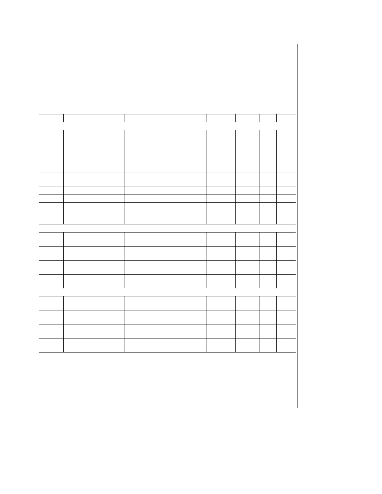
DC Electrical Characteristics Min/Max limits apply across temperature range unless otherwise noted
Symbol Parameter Conditions Min Typ Max Units
CMOS TO CMOS
V
IN(1)
V
IN(0)
V
OUT(1)
V
OUT(0)
I
IN(1)
I
IN(0)
I
OZ
I
CC
Logical ‘‘1’’ Input Voltage V
Logical ‘‘0’’ Input Voltage V
Logical ‘‘1’’ Output Voltage V
Logical ‘‘0’’ Output Voltage V
Logical ‘‘1’’ Input Current V
Logical ‘‘0’’ Input Current
Output Current in High V
Impedance State V
Supply Current V
TTL INTERFACE
V
IN(1)
V
IN(0)
V
OUT(1)
V
OUT(0)
Logical ‘‘1’’ Input Voltage 70C V
Logical ‘‘0’’ Input Voltage 70C V
Logical ‘‘1’’ Output Voltage 70C V
Logical ‘‘0’’ Output Voltage 70C V
OUTPUT DRIVE (Short Circuit Current)
I
SOURCE
I
SOURCE
I
SINK
I
SINK
Note 1: ‘‘Absolute Maximum Ratings’’ are those values beyond which the safety of the device cannot be guaranteed. Except for ‘‘Operating Temperature Range’’
they are not meant to imply that the device should be operated at these limits. The table of ‘‘Electrical Characteristics’’ provides conditions for actual device
operation.
Note 2: Capacitance is guaranteed by periodic testing.
Note 3: C
AN-90.
Output Source Current V
Output Source Current V
Output Sink Current V
Output Sink Current V
determines the no load AC power consumption of any CMOS device. For complete explanation see 54C/74C Family Characteristics application note
PD
e
5V 3.5 V
CC
e
V
10V 8.0 V
CC
e
5V 1.5 V
CC
e
V
10V 2.0 V
CC
e
5V 4.5 V
CC
e
V
10V 9.0 V
CC
e
5V 0.5 V
CC
e
V
10V 1.0 V
CC
e
15V 0.005 1.0 mA
CC
b
1.0
e
CC
e
CC
e
CC
80C V
80C V
80C V
80C V
e
CC
e
25§C, V
T
A
e
CC
e
25§C, V
T
A
e
CC
e
T
25§C, V
A
e
CC
e
T
25§C, V
A
e
15V, V
15V, V
15V 0.005 1.0 mA
O
e
0V
O
b
1.0
15V 0.01 15 mA
e
4.5V V
CC
e
4.75V V
CC
e
4.5V 0.8 V
CC
e
4.75V 0.8 V
CC
CC
CC
CC
CC
5V, V
10V, V
5V, V
10V, V
e
e
e
e
IN(1)
OUT
IN(1)
OUT
IN(0)
OUT
IN(0)
OUT
4.5V, I
4.75V, I
4.5V, I
4.75V, I
e
5V
e
0V
e
e
0V
e
0V
e
V
e
e
V
eb
1.6 mA 2.4 V
O
eb
1.6 mA 2.4 V
O
e
1.6 mA 0.4 V
O
e
1.6 mA 0.4 V
O
10V
CC
0V
CC
b
CC
b
CC
b
4.35 mA
b
20 mA
4.35 mA
20 mA
b
0.005 mA
b
0.005 mA
1.5 V
1.5 V
C
§
2
Page 3
AC Electrical Characteristics* T
e
A
25§C, C
e
50 pF, unless otherwise noted.
L
Symbol Parameter Conditions Min Typ Max Units
t
pd0,tpd1
t
pd0,tpd1
t1H,t
tH1,t
C
IN
C
OUT
C
PD
*AC Parameters are guaranteed by DC correlated testing.
Propagation Delay Time to a Logical ‘‘0’’ or
Logical ‘‘1’’ from Data Input to Output
MM70C95/MM80C95, MM70C97/MM80C97 V
MM70C96/MM80C96, MM70C98/MM80C98 V
e
5V 60 100 ns
CC
e
V
10V 25 40 ns
CC
e
5V 70 150 ns
CC
e
V
10V 35 75 ns
CC
Propagation Delay Time to a Logical ‘‘0’’ or
Logical ‘‘1’’ from Data Input to Output
MM70C95/MM80C95, MM70C97/MM80C97 V
MM70C96/MM80C96, MM70C98/MM80C98 V
Delay from Disable Input to High Impedance
0H
State, (from Logical ‘‘1’’ or Logical ‘‘0’’)
MM70C95/MM80C95 V
MM70C96/MM80C96 V
MM70C97/MM80C97 V
MM70C98/MM80C98 V
Delay from Disable Input to Logical ‘‘1’’ Level
H0
(from High Impedance State)
MM70C95/MM80C95 V
MM70C96/MM80C96 V
MM70C97/MM80C97 V
MM70C98/MM80C98 V
e
CC
e
V
CC
e
CC
e
V
CC
e
R
L
e
CC
e
V
CC
e
CC
e
V
CC
e
CC
e
V
CC
e
CC
e
V
CC
e
R
L
e
CC
e
V
CC
e
CC
e
V
CC
e
CC
e
V
CC
e
CC
e
V
CC
e
5V, C
10V, C
5V, C
10V, C
10k, C
150 pF 85 160 ns
L
e
150 pF 40 80 ns
L
e
150 pF 95 210 ns
L
e
150 pF 45 110 ns
L
e
5pF
L
5V 80 135 ns
10V 50 90 ns
5V 100 180 ns
10V 70 125 ns
5V 70 125 ns
10V 50 90 ns
5V 90 170 ns
10V 70 125 ns
e
10k, C
50 pF
L
5V 120 200 ns
10V 50 90 ns
5V 130 225 ns
10V 60 110 ns
5V 95 175 ns
10V 40 80 ns
5V 120 200 ns
10V 50 90 ns
Input Capacitance Any Input (Note 2) 5.0 pF
Output Capacitance TRI-STATE Any Output (Note 2) 11 pF
Power Dissipation Capacitance (Note 3) 60 pF
Truth Tables
MM70C95/MM80C95
Disable Input
DIS
1
DIS
2
Input Output
0000
0011
0 1 X H-z
1 0 X H-z
1 1 X H-z
Disable Input
DIS
1
0001
0010
0 1 X H-z
1 0 X H-z
1 1 X H-z
MM70C96/MM80C96
DIS
2
Input Output
MM70C97/MM80C97
Disable Input
DIS
4
DIS
2
Input Output
0000
0011
X 1 X H-z*
1 X X H-z**
*Output 5– 6 only
**Output 1– 4 only
e
Irrelevant
X
Disable Input
DIS
3
MM70C98/MM80C98
4
DIS
2
Input Output
0001
0010
X 1 X H-z*
1 X X H-z**
Page 4

AC Test Circuits and Switching Time Waveforms
t
pd0,tpd1
TL/F/5907– 13
CMOS to CMOS
TL/F/5907– 14
t1Hand t
H1
TL/F/5907– 15
t0Hand t
H0
Note: Delays measured with input tr,t
TL/F/5907– 18
t
1H
TL/F/5907– 16
t
0H
TL/F/5907– 19
s
20 ns.
f
t
H1
TL/F/5907– 17
t
H0
TL/F/5907– 20
4
Page 5

Typical Performance Characteristics
Propagation Delay vs
Load Capacitance
Dtpd/pF vs
Power Supply Voltage
N-Channel Output Drive at 25§C
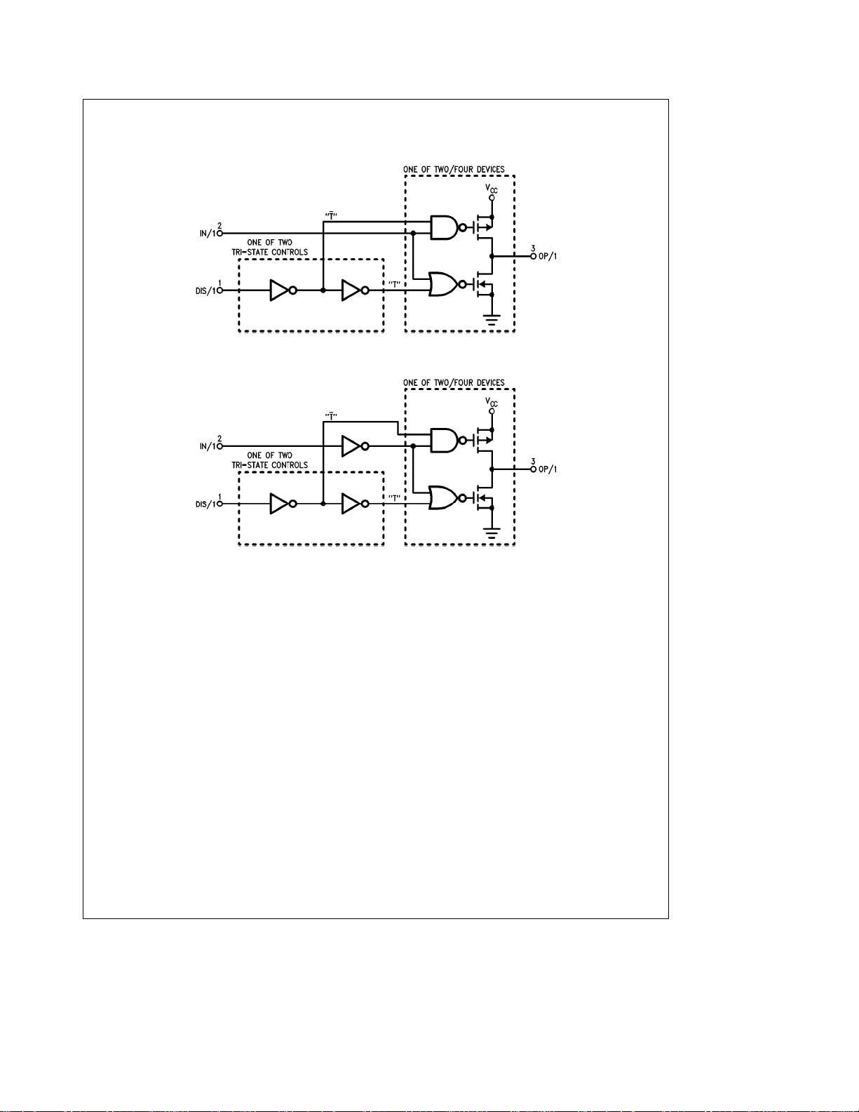
Schematic Diagrams
TL/F/5907– 5
TL/F/5907– 7
MM70C95/MM80C95 TRI-STATE
MM70C96/MM80C96 TRI-STATE
TL/F/5907– 6
P-Channel Output Drive at 25§C
TL/F/5907– 8
TL/F/5907– 9
TL/F/5907– 10
5
Page 6
Schematic Diagrams (Continued)
MM70C97/MM80C97 TRI-STATE
TL/F/5907– 11
MM70C98/MM80C98 TRI-STATE
TL/F/5907– 12
6
Page 7

Physical Dimensions inches (millimeters)
Order Number MM70C95J, MM70C96J, MM70C97J, MM70C98J,
Ceramic Dual-In-Line Package (J)
MM80C95J, MM80C96J, MM80C97J or MM80C98J
NS Package Number J16A
7
Page 8

Physical Dimensions inches (millimeters) (Continued)
Order Number MM70C95N, MM70C96N, MM70C97N, MM70C98N,
Molded Dual-In-Line Package (N)
MM80C95N, MM80C96N, MM80C97N or MM80C98N
NS Package Number N16E
MM70C95/MM80C95, MM70C97/MM80C97 TRI-STATE Hex Buffers
MM70C96/MM80C96, MM70C98/MM80C98 TRI-STATE Hex Inverters
LIFE SUPPORT POLICY
NATIONAL’S PRODUCTS ARE NOT AUTHORIZED FOR USE AS CRITICAL COMPONENTS IN LIFE SUPPORT
DEVICES OR SYSTEMS WITHOUT THE EXPRESS WRITTEN APPROVAL OF THE PRESIDENT OF NATIONAL
SEMICONDUCTOR CORPORATION. As used herein:
1. Life support devices or systems are devices or 2. A critical component is any component of a life
systems which, (a) are intended for surgical implant support device or system whose failure to perform can
into the body, or (b) support or sustain life, and whose be reasonably expected to cause the failure of the life
failure to perform, when properly used in accordance support device or system, or to affect its safety or
with instructions for use provided in the labeling, can effectiveness.
be reasonably expected to result in a significant injury
to the user.
National Semiconductor National Semiconductor National Semiconductor National Semiconductor
Corporation Europe Hong Kong Ltd. Japan Ltd.
1111 West Bardin Road Fax: (
Arlington, TX 76017 Email: cnjwge@tevm2.nsc.com Ocean Centre, 5 Canton Rd. Fax: 81-043-299-2408
Tel: 1(800) 272-9959 Deutsch Tel: (
Fax: 1(800) 737-7018 English Tel: (
National does not assume any responsibility for use of any circuitry described, no circuit patent licenses are implied and National reserves the right at any time without notice to change said circuitry and specifications.
Fran3ais Tel: (
Italiano Tel: (
a
49) 0-180-530 85 86 13th Floor, Straight Block, Tel: 81-043-299-2309
a
49) 0-180-530 85 85 Tsimshatsui, Kowloon
a
49) 0-180-532 78 32 Hong Kong
a
49) 0-180-532 93 58 Tel: (852) 2737-1600
a
49) 0-180-534 16 80 Fax: (852) 2736-9960
 Loading...