

Page 1
TL/F/5908
MM78C29/MM88C29 Quad Single-Ended Line Driver
MM78C30/MM88C30 Dual Differential Line Driver
February 1996
MM78C29/MM88C29 Quad Single-Ended Line Driver
MM78C30/MM88C30 Dual Differential Line Driver
General Description
The MM78C30/MM88C30 is a dual differential line driver
that also performs the dual four-input NAND or dual four-input AND function. The absence of a clamp diode to V
CC
in
the input protection circuitry of the MM78C30/MM88C30 allows a CMOS user to interface systems operating at different voltage levels. Thus, a CMOS digital signal source can
operate at a V
CC
voltage greater than the VCCvoltage of
the MM78C30 line driver. The differential output of the
MM78C30/MM88C30 eliminates ground-loop errors.
The MM78C29/MM88C29 is a non-inverting single-wire
transmission line driver. Since the output ON resistance is a
low 20X typ., the device can be used to drive lamps, relays,
solenoids, and clock lines, besides driving data lines.
Features
Y
Wide supply voltage range 3V to 15V
Y
High noise immunity 0.45 VCC(typ.)
Y
Low output ON resistance 20X (typ.)
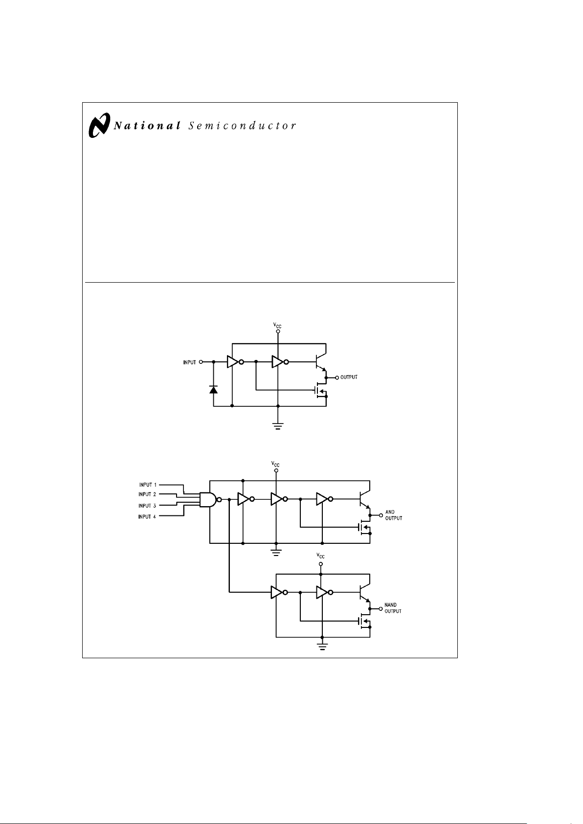
Logic Diagrams
1/4 MM78C29/MM88C29
TL/F/5908– 1
1/2 MM78C30/MM88C30
TL/F/5908– 2
C
1996 National Semiconductor Corporation RRD-B30M36/Printed in U. S. A.
http://www.national.com
Page 2
Absolute Maximum Ratings (Note 1)
If Military/Aerospace specified devices are required,
please contact the National Semiconductor Sales
Office/Distributors for availability and specifications.
Voltage at Any Pin (Note 1)
b
0.3V to V
CC
a
16V
Operating Temperature Range
MM78C29/MM78C30
b
55§Ctoa125§C
MM88C29/MM88C30
b
40§Ctoa85§C
Storage Temperature
b
65§Ctoa150§C
Power Dissipation (PD)
Dual-In-Line 700 mW
Small Outline 500 mW
Operating V
CC
Range 3V to 15V
Absolute Maximum V
CC
18V
Average Current at Output
MM78C30/MM88C30 50 mA
MM78C29/MM88C29 25 mA
Maximum Junction Temperature, T
j
150§C
Lead Temperature
(Soldering, 10 seconds) 260
§
C
DC Electrical Characteristics Min/Max limits apply across temperature range unless otherwise noted
Symbol Parameter Conditions Min Typ Max Units
CMOS TO CMOS
V
IN(1)
Logical ‘‘1’’ Input Voltage V
CC
e
5V 3.5 V
V
CC
e
10V 8 V
V
IN(0)
Logical ‘‘0’’ Input Voltage V
CC
e
5V 1.5 V
V
CC
e
10V 2 V
I
IN(1)
Logical ‘‘1’’ Input Current V
CC
e
15V, V
IN
e
15V 0.005 1 mA
I
IN(0)
Logical ‘‘0’’ Input Current V
CC
e
15V, V
IN
e
0V
b
1
b
0.005 mA
I
CC
Supply Current V
CC
e
5V 0.05 100 mA
OUTPUT DRIVE
I
SOURCE
Output Source Current
MM78C29/MM78C30 V
OUT
e
V
CC
b
1.6V,
V
CC
t
4.5V, T
j
e
25§C
b
57
b
80 mA
T
j
e
125§C
b
32
b
50 mA
MM88C29/MM88C30 V
OUT
e
V
CC
b
1.6V,
V
CC
t
4.75V, T
j
e
25§C
b
47
b
80 mA
T
j
e
85§C
b
32
b
60 mA
MM78C29/MM88C29 V
OUT
e
V
CC
b
0.8V
b
2
b
20 mA
MM78C30/MM88C30 V
CC
t
4.5V
I
SINK
Output Sink Current
MM78C29/MM78C30 V
OUT
e
0.4V, V
CC
e
4.5V,
T
j
e
25§C1120mA
T
j
e
125§C 8 14 mA
V
OUT
e
0.4V, V
CC
e
10V,
T
j
e
25§C2240mA
T
j
e
125§C1628mA
MM88C29/MM88C30 V
OUT
e
0.4V, V
CC
e
4.75V,
T
j
e
25§C 9.5 22 mA
T
j
e
85§C 8 18 mA
V
OUT
e
0.4V, V
CC
e
10V,
T
j
e
25§C1940mA
T
j
e
125§C 15.5 33 mA
I
SOURCE
Output Source Resistance
MM78C29/MM78C30 V
OUT
e
V
CC
b
1.6V,
V
CC
t
4.5V, T
j
e
25§C2028X
T
j
e
125§C3250X
MM88C29/MM88C30 V
OUT
e
V
CC
b
1.6V,
V
CC
t
4.75V, T
j
e
25§C2034X
T
j
e
85§C2750X
http://www.national.com 2
Page 3
DC Electrical Characteristics
Min/Max limits apply across temperature range, unless otherwise noted (Continued)
Symbol Parameter Conditions Min Typ Max Units
OUTPUT DRIVE (Continued)
I
SINK
Output Sink Resistance
MM78C29/MM78C30 V
OUT
e
0.4V, V
CC
e
4.50V,
T
j
e
25§C2036X
T
j
e
125§C2850X
V
OUT
e
0.4V, V
CC
e
10V,
T
j
e
25§C1018X
T
j
e
125§C1425X
MM88C29/MM88C30 V
OUT
e
0.4V, V
CC
e
4.75V,
T
j
e
25§C1841X
T
j
e
85§C2250X
V
OUT
e
0.4V, V
CC
e
10V,
T
j
e
25§C1021X
T
j
e
85§C1226X
Output Resistance
Temperature Coefficient
Source 0.55 %/
§
C
Sink 0.40 %/
§
C
i
JA
Thermal Resistance
MM78C29/MM78C30 100
§
C/W
(D-Package)
MM88C29/MM88C30
150
§
C/W
(N-Package)
AC Electrical Characteristics* T
A
e
25§C, C
L
e
50 pF
Symbol Parameter Conditions Min Typ Max Units
t
pd
Propagation Delay Time to
Logical ‘‘1’’ or ‘‘0’’ (See
Figure 2
)
MM78C29/MM88C29 V
CC
e
5V 80 200 ns
V
CC
e
10V 35 100 ns
MM78C30/MM88C30 V
CC
e
5V 110 350 ns
V
CC
e
10V 50 150 ns
t
pd
Differential Propagation Delay R
L
e
100X,C
L
e
5000 pF
Time to Logical ‘‘1’’ or ‘‘0’’ (See
Figure 1
)
MM78C30/MM88C30 V
CC
e
5V 400 ns
V
CC
e
10V 150 ns
C
IN
Input Capacitance
MM78C29/MM88C29 (Note 3) 5.0 pF
MM78C30/MM88C30 (Note 3) 5.0 pF
C
PD
Power Dissipation Capacitance
MM78C29/MM88C29 (Note 3) 150 pF
MM78C30/MM88C30 (Note 3) 200 pF
*AC Parameters are guaranteed by DC correlated testing.
Note 1: ‘‘Absolute Maximum Ratings’’ are those values beyond which the safety of the device cannot be guaranteed. Except for ‘‘Operating Temperature Range’’
they are not meant to imply that the devices should be operated at these limits. The table of ‘‘Electrical Characteristics’’ provides conditions for actual device
operation.
Note 2: Capacitance is guaranteed by periodic testing.
Note 3: C
PD
determines the no load AC power consumption of any CMOS device. For complete explanation see 54C/74C Family Characteristics application note
AN-90 (CMOS Logic Databook).
http://www.national.com3
Page 4

Connection Diagrams
Dual-In-Line Package
MM78C29/MM88C29
TL/F/5908– 3
Top View
Order Number MM88C29M or MM88C29N
Dual-In-Line Package
MM78C30/MM88C30
TL/F/5908– 4
Top View
Order Number MM88C30M or MM88C30N
For Complete Military 883 Specifications, see RETS Data Sheet.
Order Number MM78C29J/883, MM78C29W/883, MM78C30J/883 or MM78C30W/883
Typical Performance Characteristics
Load Capacitance
Typical Propagation Delay vs
MM78C29/MM88C29
Load Capacitance
Typical Propagation Delay vs
MM78C29/MM88C29
Load Capacitance
Typical Propagation Delay vs
MM78C30/MM88C30
Load Capacitance
Typical Propagation Delay vs
MM78C30/MM88C30
Output Voltage
Typical Sink Current vs
Output Voltage
Typical Source Current vs
TL/F/5908– 5
http://www.national.com 4
Page 5

AC Test Circuits
TL/F/5908– 6
TL/F/5908– 7
FIGURE 1
TL/F/5908– 8 TL/F/5908– 9
FIGURE 2
Typical Applications
Digital Data Transmission
TL/F/5908– 10
Note 1: Exact value depends on line length.
Note 2: Optional to control response time.
Note 3: V
CC
e
4.5V to 5.5V for the DS7820, V
CC
e
4.5V to 15V for the
DS78C20.
http://www.national.com5
Page 6

Typical Applications (Continued)
TL/F/5908– 11
TL/F/5908– 12
Note 1: VCCis 3V to 15V
Typical Data Rate vs Transmission Line Length
TL/F/5908– 13
Note 1: The transmission line used wasÝ22 gauge unshielded twisted pair (40k
termination).
Note 2: The curves generated assume that both drivers are driving equal lines,
and that the maximum power is 500 mW/package.
http://www.national.com 6
Page 7

Physical Dimensions inches (millimeters)
Ceramic Dual-In-Line Package (J)
Order Number MM78C29J, MM78C30J, MM88C29J or MM88C30J
NS Package Number J14A
http://www.national.com7
Page 8

MM78C29/MM88C29 Quad Single-Ended Line Driver
MM78C30/MM88C30 Dual Differential Line Driver
Physical Dimensions inches (millimeters) (Continued)
Molded Dual-In-Line Package (N)
Order Number MM78C29N, MM78C30N, MM88C29N or MM88C30N
NS Package Number N14A
LIFE SUPPORT POLICY
NATIONAL’S PRODUCTS ARE NOT AUTHORIZED FOR USE AS CRITICAL COMPONENTS IN LIFE SUPPORT
DEVICES OR SYSTEMS WITHOUT THE EXPRESS WRITTEN APPROVAL OF THE PRESIDENT OF NATIONAL
SEMICONDUCTOR CORPORATION. As used herein:
1. Life support devices or systems are devices or 2. A critical component is any component of a life
systems which, (a) are intended for surgical implant support device or system whose failure to perform can
into the body, or (b) support or sustain life, and whose be reasonably expected to cause the failure of the life
failure to perform, when properly used in accordance support device or system, or to affect its safety or
with instructions for use provided in the labeling, can effectiveness.
be reasonably expected to result in a significant injury
to the user.
National Semiconductor National Semiconductor National Semiconductor National Semiconductor
Corporation Europe Hong Kong Ltd. Japan Ltd.
1111 West Bardin Road Fax:
a
49 (0) 180-530 85 86 13th Floor, Straight Block, Tel: 81-043-299-2308
Arlington, TX 76017 Email: europe.support@nsc.com Ocean Centre, 5 Canton Rd. Fax: 81-043-299-2408
Tel: 1(800) 272-9959 Deutsch Tel:
a
49 (0) 180-530 85 85 Tsimshatsui, Kowloon
Fax: 1(800) 737-7018 English Tel:
a
49 (0) 180-532 78 32 Hong Kong
Fran3ais Tel:
a
49 (0) 180-532 93 58 Tel: (852) 2737-1600
http://www.national.com
Italiano Tel:a49 (0) 180-534 16 80 Fax: (852) 2736-9960
National does not assume any responsibility for use of any circuitry described, no circuit patent licenses are implied and National reserves the right at any time without notice to change said circuitry and specifications.
 Loading...