

Datasheet MM74HCT574WMX, MM74HCT574SJ, MM74HCT574SJX, MM74HCT574MTCX, MM74HCT574CW Datasheet (Fairchild Semiconductor)
...Page 1
February 1990
Revised May 1999
MM74HCT573 • MM74HCT574 Octal D-Type Latch • 3-STATE Octal D-Type Flip-Flop
© 1999 Fairchild Semiconductor Corporation DS010627.prf www.fairchildsemi.com
MM74HCT573 • MM74HCT574
Octal D-Type Latch • 3-STATE Octal D-Type Flip-Flop
General Description
The MM74HCT573 octal D-type latches and
MM74HCT574 octal D-type flip-flop advanced silicon-gate
CMOS technology, which provides the inherent benefits of
low power consumption and w ide power su pply range, but
are LS-TTL input and output characteristic and pin-out
compatible. The 3-STATE outputs are capable of driving 15
LS-TTL loads. All inputs are protected from damage due to
static discharge by internal diodes to V
CC
and ground.
When the MM74HCT573 Latch Enable in put is HIGH, the
Q outputs will follow the D inputs. When the Latch Enable
goes LOW, data at the D inputs will be retained at the outputs until Latch Enable retu rns HIGH again. When a high
logic level is applied to the Output Control input, all outputs
go to a high impedan ce state, regardless of wha t signals
are present at the other inputs and the state of the storage
elements.
The MM74HCT574 a re positive edge triggered flip-fl ops.
Data at the D inputs, meeting the setup and hold time
requirements, are transferred to the Q outputs on positive
going transitions of the Clock (CK) input. When a high logic
level is applied to the Output Control (OC) input, all outputs
go to a high impeda nce state, regardless of wh at signals
are present at t he other inputs and the sta t e of th e s t or age
elements.
The MM74HCT devi ces are intended to inter face bet ween
TTL and NMOS components and standard CMOS devices.
These parts are also plug in replacements for LS-TTL
devices and can be used to reduce pow er consumption in
existing designs.
Features
■ TTL input characteristic compatible
■ Typical propagation delay: 18 ns
■ Low input current: 1 µA maximum
■ Low quiescent current: 80 µA maximum
■ Compatible with bus-oriented systems
■ Output drive capability: 15 LS-TTL loads
Ordering Codes:
Devices also availab le in Tape and Reel. Specify by appending su ffix let te r “X” to the ordering code .
Order Number Package Number Package Description
MM74HCT573WM M20B 20-Lead Small Outline Integrated Circuit (SOIC), JEDEC MS-013, 0.300 Wide
MM74HCT573SJ M20D 20-Lead Small Outline Package (SOP), EIAJ TYPE II, 5.3mm Wide
MM74HCT573MTC MTC20 20-Lead Thin Shrink Small Outline Package (TSSOP), JEDEC MO-153, 4.4mm Wide
MM74HCT573N N20A 20-Lead Plastic Dual-In-Line Package (PDIP), JEDEC MS-001, 0.300 Wide
MM74HCT574WM M20B 20-Lead Small Outline Integrated Circuit (SOIC), JEDEC MS-013, 0.300 Wide
MM74HCT574SJ M20D 20-Lead Small Outline Package (SOP), EIAJ TYPE II, 5.3mm Wide
MM74HCT574MTC MTC20 20-Lead Thin Shrink Small Outline Package (TSSOP), JEDEC MO-153, 4.4mm Wide
MM74HCT574N N20A 20-Lead Plastic Dual-In-Line Package (PDIP), JEDEC MS-001, 0.300 Wide
Page 2
www.fairchildsemi.com 2
MM74HCT573 • MM74HCT574
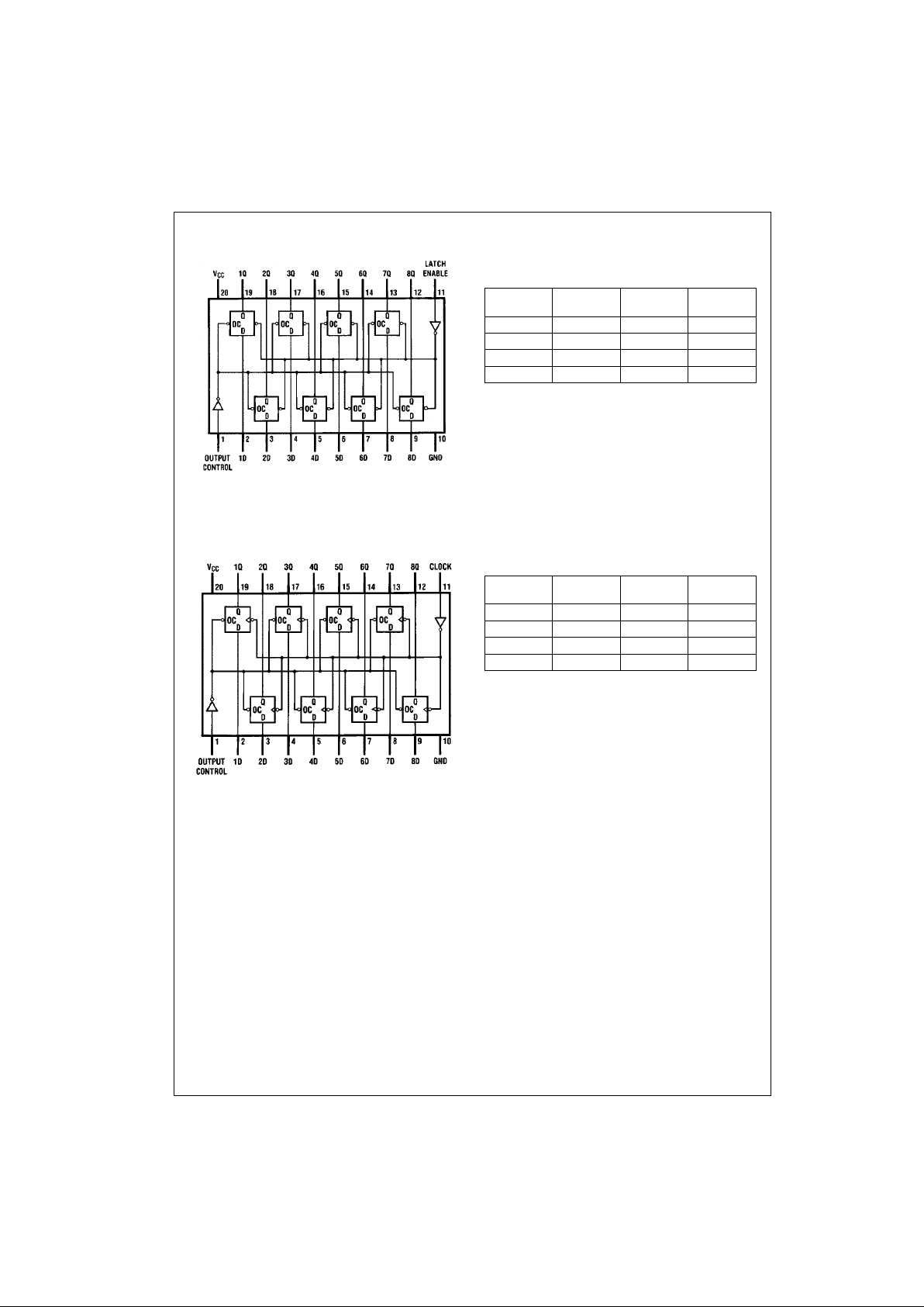
Connection Diagrams
Top View
MM74HCT573
Top View
MM74HCT574
Tr uth Tables
MM74HCT573
H = HIGH Level
L = LOW Level
Q0 = Level of output before steady-state input conditions were est ablished.
Z = High Impedance State
MM74HCT574
H = HIGH Level
L = LOW Level
Q0 = Level of output before steady-state input conditions were est ablished.
X = Don’t Care
Z = High Impedance State
↑ = Transition from LOW-to-HIGH
Output
Control
LE Data Output
LHHH
LHLL
LLXQ
0
HXXZ
Output
Control
LE Data Output
L ↑ HH
L ↑ LL
LLXQ
0
HXXZ
Page 3
3 www.fairchildsemi.com
MM74HCT573 • MM74HCT574
Absolute Maximum Ratings(Note 1)
(Note 2)
Recommended Operating
Conditions
Note 1: Absolute Maximum Ra tings are those valu es beyond w hich dam-
age to the device may occur.
Note 2: Unless otherwise specified all voltages are referenced to ground.
Note 3: Power Dissipation te mperature d erating — pl astic “N” pa ckage: −
12 mW/°C from 65°C to 85°C.
DC Electrical Characteristics
VCC = 5V ± 10% (unless otherwise specified)
Note 4: Measured pe r pin. All others tied to VCC or ground.
Supply Voltage (VCC) −0.5 to +7.0V
DC Input Voltage (V
IN
) −1.5 to VCC+ 1.5V
DC Output Voltage (V
OUT
) −0.5 to VCC+ 0.5V
Clamp Diode Current (I
IK
, IOK) ± 20 mA
DC Output Current, per pin (I
OUT
) ± 35 mA
DC V
CC
or GND Current, per pin (ICC) ± 70 mA
Storage Temperature Range (T
STG
) −65°C to +150°C
Power Dissipation (P
D
)
(Note 3) 600 mW
S. O. Package only 500 mW
Lead Temperature (T
L
)
(Solderi ng 10 seconds) 260°C
Min Max Units
Supply Voltage (V
CC
)4.55.5V
DC Input or Output Voltage
(V
IN
, V
OUT
)0V
CC
V
Operating Temperature Range (T
A
) −40 +85 °C
Input Rise or Fall Times
t
r
, t
f
500 ns
Symbol Parameter Conditions
TA = 25°CTA = −40 to 85°CTA = −55 to 125°C
Units
Typ Guaranteed Limits
V
IH
Minimum HIGH Level
2.0 2.0 2.0 V
Input Voltage
V
IL
Maximum LOW Level
0.8 0.8 0.8 V
Input Voltage
V
OH
Minimum HIGH Level VIN = VIH or V
IL
V
Output Voltage |I
OUT
| = 20 µAV
CCVCC
− 0.1 VCC − 0.1 VCC − 0.1
|I
OUT
| = 6.0 mA, VCC = 4.5V 4.2 3.98 3.84 3.7
|I
OUT
| = 7.2 mA, VCC = 5.5V 5.7 4.98 4.84 4.7
V
OL
Maximum LOW Level VIN = VIH or V
IL
V
Voltage |I
OUT
| = 20 µA 0 0.1 0.1 0.1
|I
OUT
| = 6.0 mA, VCC = 4.5V 0.2 0.26 0.33 0.4
|I
OUT
| = 7.2 mA, VCC = 5.5V 0.2 0.26 0.33 0.4
I
IN
Maximum Input VIN = VCC or GND,
±0.1 ±1.0 ±1.0 µA
Current VIH or V
IL
I
OZ
Maximum 3-STATE V
OUT
= VCC or GND
±0.5 ±5.0 ±10 µAOutput Leakage Enable = VIH or V
IL
Current
I
CC
Maximum Quiescent VIN = VCC or GND
8.0 80 160 µA
Supply Current I
OUT
= 0 µA
VIN = 2.4V or 0.5V (Note 4) 1.5 1.8 2.0 mA
Page 4
www.fairchildsemi.com 4
MM74HCT573 • MM74HCT574
AC Electrical Characteristics MM74HCT573
VCC = 5.0V, tr = tf = 6 ns, TA = 25°C (unless otherwise specified)
AC Electrical Characteristics MM74HCT573
V
CC
= 5.0V ± 10%, tr = t
f
= 6 ns (unless otherwise specified)
Note 5: CPD determines the no lo ad dynamic power con s um ption, PD = CPD VCC2 f+ICC VCC, and the no load dynam ic current consumpt ion,
I
S
= CPDVCCf+ICC.
Symbol Parameter Conditions Typ Guaranteed Limit Units
t
PHL
Maximum Propagation Delay CL = 45 pF
17 27 ns
t
PLH
Data to Output
t
PHL
Maximum Propagation Delay CL = 45 pF
16 27 ns
t
PLH
Latch Enable to Output
t
PZH
Maximum Enable Propagation Delay CL = 45 pF
21 30 ns
t
PZL
Control to Output RL = 1 kΩ
t
PHZ
Maximum Disable Propagation Delay CL = 5 pF
14 23 ns
t
PLZ
Control to Output RL = 1 kΩ
t
W
Minimum Clock Pulse Width 15 ns
t
S
Minimum Setup Time Data to Clock 5 ns
t
H
Minimum Hold Time Clock to Data 12 ns
Symbol Parameter Conditions
TA = 25° TA = −40 to 85°CTA = −55 to 125°C
Units
Typ Guaranteed Limits
t
PHL
Maximum Propagation CL = 50 pF
18 30 38 45 ns
t
PLH
Delay Data to Output
t
PHL
Maximum Propagation Delay CL = 50 pF
17 30 44 53 ns
t
PLH
Latch Enable to Output
t
PZH
Maximum Enable Propagation CL = 50 pF
22 30 38 45 ns
t
PZL
Delay Control to Output RL = 1 kΩ
t
PHZ
Maximum Disable Propagation CL = 50 pF
15 30 38 45 ns
t
PLZ
Delay Control to Output RL = 1 kΩ
t
THL
Maximum Output CL = 50 pF
612 15 18 ns
t
TLH
Rise and Fall Time
t
W
Minimum Clock Pulse Width 15 20 24 ns
t
S
Minimum Setup Time Data to Clock −35 6 8 ns
t
H
Minimum Hold Time Clock to Data 4 12 15 18 ns
C
IN
Maximum Input Capacitance 10 10 10 pF
C
OUT
Maximum Output Capacitance 20 20 20 pF
C
PD
Power Dissipation Capacitance OC = V
CC
5
pF
(Note 5) OC = GND 52
Page 5

5 www.fairchildsemi.com
MM74HCT573 • MM74HCT574
AC Electrical Characteristics MM74HCT574
VCC = 5.0V, tr = tf = 6 ns, TA = 25°C
AC Electrical Characteristics MM74HCT574
VCC = 5.0V ± 10%, tr = tf = 6 ns (unless otherwise specified)
Note 6: CPD determines the no load power consumptio n, PD = CPD V
CC
2
f + ICC VCC, and the no load dynam ic cu rrent consumption, IS = CPD VCC f + ICC.
Symbol Parameter Conditions Typ Guaranteed Limit Units
f
MAX
Maximum Clock Frequency 60 33 MHz
t
PHL
Maximum Propagation Delay CL = 45 pF
17 27 ns
t
PLH
to Output
t
PZH
Maximum Enable Propagation Delay CL = 45 pF
19 28 ns
t
PZL
Control to Output RL = 1 kΩ
t
PHZ
Maximum Disable Propagation Delay CL = 45 pF
14 25 ns
t
PLZ
Control to Output RL = 1 kΩ
t
W
Minimum Clock Pulse Width 15 ns
t
S
Minimum Setup Time Data to Clock 12 ns
t
H
Minimum Hold Time Clock to Data 5 ns
Symbol Parameter Conditions
TA = 25°CTA = −40 to 85°CTA = −55 to 125°C
Units
Typ Guaranteed Limits
f
MAX
Maximum Clock Frequency 33 28 23 MHz
t
PHL
Maximum Propagation Delay CL = 50 pF
18 30 38 45 ns
t
PLH
Clock to Output
t
PZH
Maximum Enable Propagation CL = 50 pF
22 30 38 45 ns
t
PZL
Delay Control to Output RL = 1 kΩ
t
PHZ
Maximum Disable Propagation CL = 50 pF
15 30 38 45 ns
t
PLZ
Delay Control to Output RL = 1 kΩ
t
THL
Maximum Output CL = 50 pF
612 15 18 ns
t
TLH
Rise and Fall Time
t
W
Minimum Clock Pulse Width 15 20 24 ns
t
S
Minimum Setup Time Data to Clock 6 12 15 18 ns
t
H
Minimum Hold Time Clock to Data −15 6 8 ns
C
IN
Maximum Input Capacitance 10 10 10 pF
C
OUT
Maximum Output Capacitance 20 20 20 pF
C
PD
Power Dissipation Capacitance OC = V
CC
5
pF
(Note 6) OC = GND 58
Page 6

www.fairchildsemi.com 6
MM74HCT573 • MM74HCT574
Physical Dimensions inches (millimeters) unless otherwise noted
20-Lead Small Outline Integrated Circuit (SOIC), JEDEC MS-013, 0.300 Wide
Package Number M20B
20-Lead Small Outline Package (SOP), EIAJ TYPE II, 5.3mm Wide
Package Number M20D
Page 7
7 www.fairchildsemi.com
MM74HCT573 • MM74HCT574
Physical Dimensions inches (millimeters) unless otherwise noted (Continued)
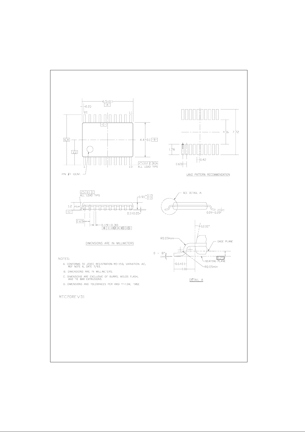
20-Lead Thin Shrink Small Outline Package (TSSOP), JEDEC MO-153, 4.4mm Wide
Package Number MTC20
Page 8
Fairchild does not assume any responsibility for use of any circuitry described, no circuit patent licenses are implied and Fairchild reserves the right at any time without notice to change said circuitry and specifications.
MM74HCT573 • MM74HCT574 Octal D-Type Latch • 3-STATE Octal D-Type Flip-Flop
LIFE SUPPORT POLICY
FAIRCHILD’S PRODUCTS ARE NOT AUTHORIZED FOR USE AS CRITICAL COMPONENTS IN LIFE SUPPORT
DEVICES OR SYSTEMS WITHOUT THE EXPRESS WRITTEN APPROVAL OF THE PRESIDENT OF FAIRCHILD
SEMICONDUCTOR CORPORATION. As used herein:
1. Life support devices or systems are devices or syste ms
which, (a) are intended for surgical implant into the
body, or (b) support or sustain life, and (c) whose failure
to perform when properly used in accordance with
instructions for use provided in the labeling, can be reasonably expected to result in a significant inju ry to the
user.
2. A critical component i n any compon ent of a lif e support
device or system whose failu re to perform can be reasonably expected to ca use the fa i lure of the life su pp ort
device or system, or to affect its safety or effectiveness.
www.fairchildsemi.com
Physical Dimensions inches (millimeters) unless otherwise noted (Continued)
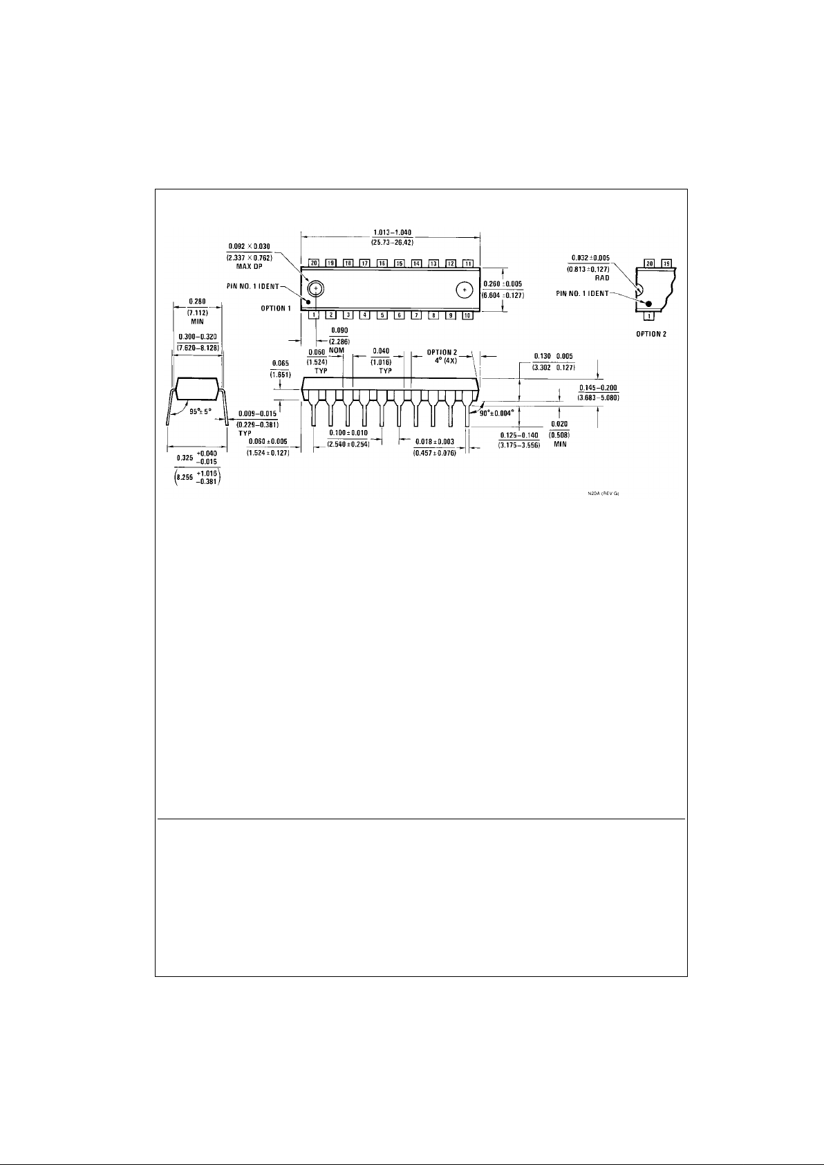
20-Lead Plastic Dual-In-Line Package (PDIP), JEDEC MS-001, 0.300 Wide
Package Number N20A
 Loading...