Datasheet MM74HCT32N, MM74HCT32SJ, MM74HCT32SJX, MM74HCT32MTC, MM74HCT32MX Datasheet (Fairchild Semiconductor)
...Page 1

October 1987
Revised February 1999
MM74HCT32 Quad 2-Input OR Gate
© 1999 Fairchild Semiconductor Corporation DS009396.prf www.fairchildsemi.com
MM74HCT32
Quad 2-Input OR Gate
General Description
The MM74HCT32 is a logic function fabricated by using
advanced silicon-gate CMOS technology, which provides
the inherent benefit s of CMOS—low qui escent power and
wide power supply range. This device is input and outp ut
characteristic and pin-out compatible with standar d 74LS
logic families. All inputs are protected from static discharge
damage by internal diodes to V
CC
and ground.
MM74HCT devices are intended to i nterface between TTL
and NMOS components and standard CMOS devices.
These parts are also plug-in replacements for LS-TTL
devices and can be used to redu ce power consumption in
existing designs.
Features
■ TTL, LS pin-out and threshold compatible
■ Fast switching: t
PLH
, t
PHL
= 10 ns (typ)
■ Low power: 10 µW at DC
■ High fan-out, 10 LS-TTL loads
Ordering Code:
Devices also available in Tape and Reel. Specify by appending suffix the letter “X” to the ordering code.
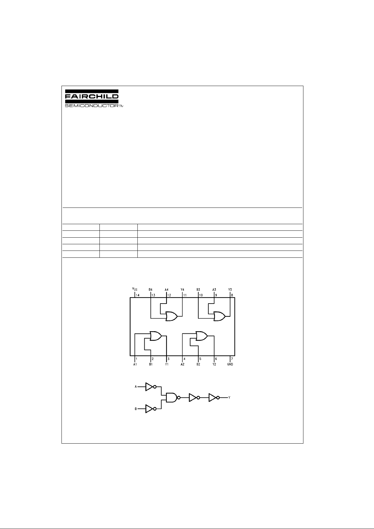
Connection Diagram
Pin Assignments for DIP, SOIC, SOP and TSSOP
Logic Diagram
Order Number Package Number Package Description
MM74HCT32M M14A 14-Lead Small Outline Integrated Circuit (SOIC), JEDEC MS-120, 0.150” Narrow
MM74HCT32SJ M14D 14-Lead Small Outline Package (SOP), EIAJ TYPE II, 5.3mm Wide
MM74HCT32MTC MTC14 14-Lead Thin Shrink Small Outline Package (TSSOP), JEDEC MO-153, 4.4mm Wide
MM74HCT32N N14A 14-Lead Plastic Dual-In-Line Package (PDIP), JEDEC MS-001 0.300” Wide
Page 2

www.fairchildsemi.com 2
MM74HCT32
Absolute Maximum Ratings(Note 1)
(Note 2)
Recommended Operating
Conditions
Note 1: Absolute Maximum Ratings are those values beyond which dam-
age to the device may occur.
Note 2: Unless otherwise specified all voltages are referenced to ground.
Note 3: Power Dissipation temperat ure derat ing — plas tic “N” p ackage: −
12 mW/°C from 65 °C to 85°C.
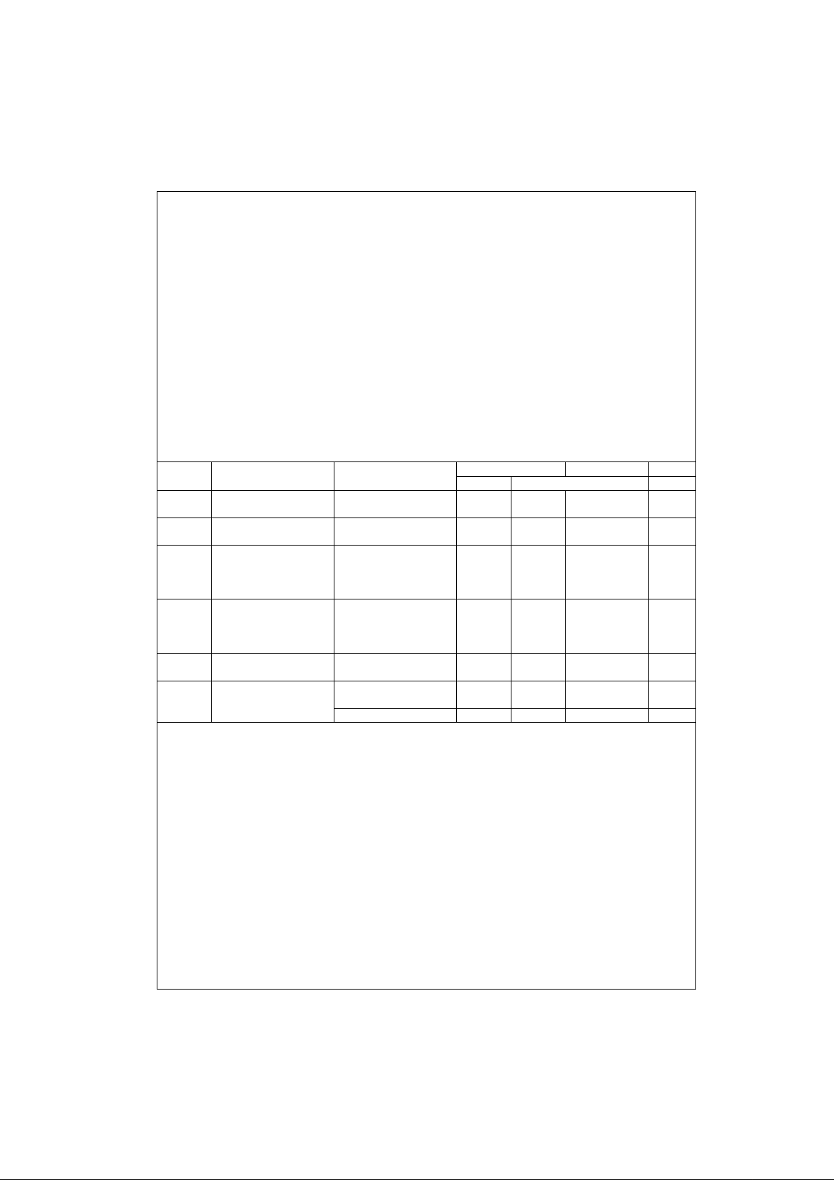
DC Electrical Characteristics
VCC = 5V ± 10% (unless otherwise specified)
Note 4: This is measured per input with all oth er inputs held at VCC or ground.
Supply Voltage (VCC) −0.5 to +7.0V
DC Input Voltage (V
IN
) −1.5 to VCC +1.5V
DC Output Voltage (V
OUT
) −0.5 to VCC +0.5V
Clamp Diode Current (I
IK
, IOK) ±20 mA
DC Output Current, per pin (I
OUT
) ±25 mA
DC V
CC
or GND Current, per pin (ICC) ±50 mA
Storage Temperature Range (T
STG
) −65°C to +150°C
Power Dissipation (P
D
)
(Note 3) 600 mW
S.O. Package only 500 mW
Lead Temperature (T
L
)
(Soldering 10 seconds) 260°C
Min Max Units
Supply Voltage (V
CC
)4.55.5V
DC Input or Output Voltage
(V
IN
, V
OUT
)0V
CC
V
Operating Temperature Range (T
A
) −40 +85 °C
Input Rise or Fall Times
(t
r
, tf)500ns
Symbol Parameter Conditions
TA = 25°CT
A
= −40°C to +85°C
Units
Typ Guaranteed Limits
V
IH
Minimum HIGH Level 2.0 2.0 V
Input Voltage
V
IL
Maximum LOW Level 0.8 0.8 V
Input Voltage
V
OH
Minimum HIGH Level VIN = VIH or V
IL
Output Voltage |I
OUT
| = 20 µAV
CC
VCC − 0.1 VCC − 0.1 V
|I
OUT
| = 4.0 mA, VCC = 4.5V 4.2 3.98 3.84 V
|I
OUT
| = 4.8 mA, VCC = 5.5V 5.2 4.98 4.84 V
V
OL
Maximum LOW Level VIN = VIH
Voltage |I
OUT
| = 20 µA00.10.1V
|I
OUT
| = 4.0 mA, VCC = 4.5V 0.2 0.26 0.33 V
|I
OUT
| = 4.8 mA, VCC = 5.5V 0.2 0.26 0.33 V
I
IN
Maximum Input VIN = VCC or GND, VIH or V
IL
± 0.1 ± 1.0 µA
Current
I
CC
Maximum Quiescent VIN = VCC or GND 2.0 20 µA
Supply Current I
OUT
= 0 µA
VIN = 2.4V or 0.5V (Note 4) 1.2 1.4 mA
Page 3

3 www.fairchildsemi.com
MM74HCT32
AC Electrical Characteristics
VCC = 5.0V, tr = tf = 6 ns, CL = 15 pF, TA = 25C° (unless otherwise noted)
AC Electrical Characteristics
VCC = 5.0V ± 10%, tr = tf = 6 ns, CL = 15 pF (unless otherwise noted)
Note 5: CPD determines th e no load dynamic power cons um ption, PD = CPD VCC2 f +ICC VCC, and the no load dynam ic c urrent consumption,
I
S
= CPD VCC f + ICC.
Symbol Parameter Conditions Typ
Guaranteed
Limit
Units
t
PLH
, t
PHL
Maximum Propagation Delay 10 ns
Symbol Parameter Conditions
TA = 25°CTA = −40°C to +85°C
Units
Typ Guaranteed Limits
t
PLH
, t
PHL
Maximum Propagation Delay 12 20 25 ns
t
THL
, t
TLH
Maximum Output Rise & Fall Time 8 15 19 ns
C
PD
Power Dissipation Capacitance (Note 5) 48 pF
C
IN
Input Capacitance 5 10 10 pF
Page 4

www.fairchildsemi.com 4
MM74HCT32
Physical Dimensions inches (millimeters) unless otherwise noted
14-Lead Small Outline Integrated Circuit (SOIC), JEDEC MS-120, 0.150” Narrow
Package Number M14A
14-Lead Small Outline Package (SOP), EIAJ TYPE II, 5.3mm Wide
Package Number M14D
Page 5

5 www.fairchildsemi.com
MM74HCT32
Physical Dimensions inches (millimeters) unless otherwise noted (Continued)
14-Lead Thin Shrink Small Outline Package (TSSOP), JEDEC MO-153, 4.4mm Wide
Package Number MTC14
Page 6

Fairchild does not assume any responsibility for use of any circuitry described, no circuit patent licenses are implied and Fairchild reserves the right at any time without notice to change said circuitry and specifications.
MM74HCT32 Quad 2-Input OR Gate
LIFE SUPPORT POLICY
FAIRCHILD’S PRODUCTS ARE NOT AUTHORIZED FOR USE AS CRITICAL COMPONENTS IN LIFE SUPPORT
DEVICES OR SYSTEMS WITHOUT THE EXPRESS WRITTEN APPROVAL OF THE PRESIDENT OF FAIRCHILD
SEMICONDUCTOR CORPORATION. As used herein:
1. Life support devices or system s ar e devices or syste ms
which, (a) are intended for surgical implant into the
body, or (b) support or sustain life, and (c) whose failure
to perform when properly used in accordance with
instructions for use provided in the labeling, can be reasonably expected to result in a significant injury to the
user.
2. A critical component in any c omponent of a life suppor t
device or system whose failure to perform can be reasonably expected to cause the failure of the life suppor t
device or system, or to affect its safety or effectiveness.
www.fairchildsemi.com
Physical Dimensions inches (millimeters) unless otherwise noted (Continued)
14-Lead Plastic Dual-In-Line Package (PDIP), JEDEC MS-001, 0.300” Wide
Package Number N14A
 Loading...