

Datasheet MM74HCT164N, MM74HCT164SJ, MM74HCT164CW, MM74HCT164SJX, MM74HCT164M Datasheet (Fairchild Semiconductor)
Page 1
February 1984
Revised February 1999
MM74HCT164 8-Bit Serial-in/Parallel-out Shift Register
© 1999 Fairchild Semiconductor Corporation DS005765.prf www.fairchildsemi.com
MM74HCT164
8-Bit Serial-in/Parallel-out Shift Register
General Description
The MM74HCT164 utilizes advanced silicon-gate CMOS
technology. It has the high noise immunity and low consumption of standard CMOS integrated circuits. It also
offers speeds comparable to low power Schottky devices.
This 8-bit shift register has ga ted ser ia l inp uts a nd CLE AR.
Each register bit is a D-type master/slave flip-flop. Inputs A
& B permit complete control over the incoming data. A
LOW at either or both inputs inhibits entr y of new data and
resets the first flip-flop to the low level at the next clock
pulse. A HIGH level on one input enables the o ther input
which will then determine the state of the first flip-flop. Data
at the serial inputs may be changed while the clock is HIGH
or LOW, but only information meeting the setup and hold
time requirements will be entered. Data is serially shifted in
and out of the 8-bit register during the positive going transition of the clock pulse. Cle ar is independent of t he clock
and accomplished by a low level at the CLEAR input.
The 74HCT logic family is f unctionally as well as pin-ou t
compatible with the standard 74LS logic family. All inputs
are protected from damage due to static discharge by internal diode clamps to V
CC
and ground.
MM74HCT devices are intended to interface between TTL
and NMOS components and standard CMOS devices.
These parts are also plug-in replacements for LS-TTL
devices and can be used to redu ce power consumption in
existing designs.
Features
■ Typical propagation delay: 20 ns
■ Low quiescent current: 40 µA maximum (74HCT Series)
■ Low input current: 1 µA maximum
■ Fanout of 10 LS-TTL loads
■ TTL input compatible
Ordering Code:
Devices also available in Tape and Reel. Specify by appending the suffix letter “X” to t he ordering code.
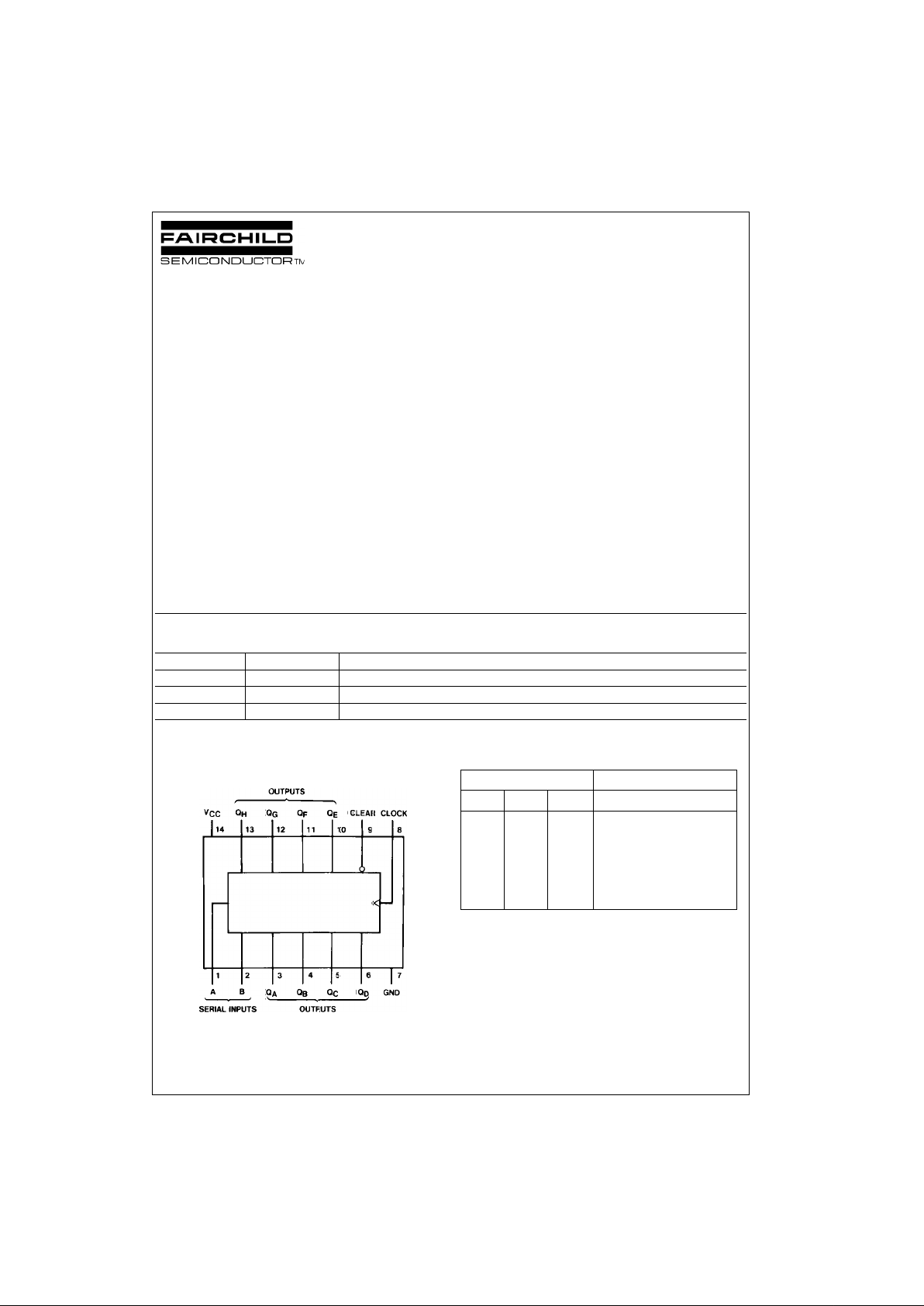
Connection Diagram
Pin Assignments for DIP, SOIC and SOP
Top View
Truth Table
H = HIGH Level (steady state)
L = LOW Level (steady state)
X = Irrelevant (any input, including trans iti ons)
↑ = Transition from LOW-to-HIGH level.
Q
AO
, QBO, QHO = the level of QA, QB, or QH, respectively, before the
indicated steady state input conditions were established.
Q
An
, QGn = The level of QA or QG before the most recent ↑ transition of
the clock; indicated a one-bit shift.
Order Number Package Number Package Description
MM74HCT164M M14A 14-Lead Small Outline Integrated Circuit (SOIC), JEDEC MS-120, 0.150” Narrow
MM74HCT164SJ M14D 14-Lead Small Outline Package (SOP), EIAJ TYPE II, 5.3mm Wide
MM74HCT164N N14A 14-Lead Plastic Dual-In-Line Package (PDIP) JEDEC MS-001, 0.300” Wide
Inputs Outputs
Clear Clock A B Q
AQB
... Q
H
LXXXLL L
HLXXQ
AOQBO
Q
HO
H ↑ HH H Q
An
Q
Gn
H ↑ LX L Q
An
Q
Gn
H ↑ XL L Q
An
Q
Gn
Page 2
www.fairchildsemi.com 2
MM74HCT164
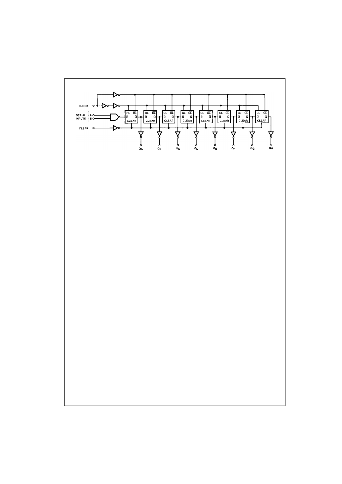
Logic Diagram
Page 3

3 www.fairchildsemi.com
MM74HCT164
Absolute Maximum Ratings(Note 1)
(Note 2)
Recommended Operating
Conditions
Note 1: Absolute Maximum Rati ngs are tho se values b eyond which d am-
age to the device may occur.
Note 2: Unless otherwise specified all voltages are referenced to ground.
Note 3: Power Dissipation temperature de rating — p lastic “N” p ackage: −
12 mW/°C from 65°C to 85°C.
DC Electrical Characteristics
V
CC
= 5V ± 10% (unless otherwise specified)
Note 4: This is measured per pin. All other input s are held at VCC ground.
Supply Voltage (VCC) −0.5 to +7.0V
DC Input Voltage (V
IN
) −1.5 to V
CC
+1.5V
DC Output Voltage (V
OUT
) −0.5 to V
CC
+0.5V
Clamp Diode Current (I
IK
, IOK) ±20 mA
DC Output Current, per pin (I
OUT
) ±25 mA
DC V
CC
or GND Current, per pin (ICC) ±50 mA
Storage Temperature Range (T
STG
) −65°C to +150°C
Power Dissipation (P
D
)
(Note 3) 600 mW
S.O. Package Only 500 mW
Lead Temperature (T
L
)
(Soldering 10 seconds) 260°C
Min Max Units
Supply Voltage (V
CC
)4.55.5V
DC Input or Output Voltage
(V
IN
, V
OUT
)0V
CC
V
Operating Temperature Range (T
A
) −40 +85 °C
Input Rise or Fall Times
(t
r
, tf) 500 ns
Symbol Parameter Conditions
TA = 25°CTA = −40 to 85°CTA = −55 to 125°C
Units
Typ Guaranteed Limits
V
IH
Minimum HIGH Level 2.0 2.0 2.0 V
Input Voltage
V
IL
Maximum LOW Level 0.8 0.8 0.8 V
Input Voltage
V
OH
Minimum HIGH Level V
IN
= VIH or V
IL
Output Voltage |I
OUT
| = 20 µAV
CCVCC
− 0.1 VCC− 0.1 VCC− 0.1 V
|I
OUT
| = 4.0 mA, VCC = 4.5V 4.2 3.98 3.84 3.7 V
|I
OUT
| = 4.8 mA, V
CC
= 5.5V 5.2 4.98 4.84 4.7 V
V
OL
Maximum LOW Level V
IN
= VIH or V
IL
Voltage |I
OUT
| = 20 µA00.10.10.1V
|I
OUT
| = 4.0 mA, V
CC
= 4.5V 0.2 0.26 0.33 0.4 V
|I
OUT
| = 4.8 mA, V
CC
= 5.5V 0.2 0.26 0.33 0.4 V
I
IN
Maximum Input V
IN
= VCC or GND ±0.1 ±1.0 ±1.0 µA
Current
I
CC
Maximum Quiescent V
IN
= VCC or GND
Supply Current I
OUT
= 0 µA8.080160µA
V
IN
= 2.4V or 0.4V (Note 4) 1.0 1.3 1.5 mA
Page 4

www.fairchildsemi.com 4
MM74HCT164
AC Electrical Charac teristics
V
CC
= 5V, TA = 25°C, CL = 15 pF, tr = t
f
= 6 ns
AC Electrical Charac teristics
V
CC
= 5.0V, ± 10%, CL = 50 pF, tr = t
f
= 6 ns (unless otherwise specified)
Note 5: CPD determines the no load dynamic power consumption, PD=CPD V
CC
2
f+ICC VCC, and the no load dynamic current consumption,
I
S=CPDVCC
f+ICC.
Symbol Parameter Conditions Typ
Guaranteed
Units
Limit
f
MAX
Maximum Operating 50% Duty 55 35 MHz
Frequency from Clock to Q Cycle Clock
t
PHL
, t
PLH
Maximum Propagation 17 27 ns
Delay Clock to Q
t
PHL
, t
PLH
Maximum Propagation 23 38 ns
Delay from Clear to Q
t
REM
Minimum Removal Time, 3 6 ns
Clear to Clock
t
S
Minimum Set Up Time tH ≥ 20 ns 6 13 ns
Data to Clock
t
H
Minimum Hold Time tS ≥ 20 ns 1.5 5 ns
Clock to Data
t
W
Minimum Pulse Width 9 16 ns
Clock, Preset or Clear
Symbol Parameter Conditions
TA = 25°CTA = −40°C to 85°CTA = −55°C to 125°C
Units
Typ Max Min Max Min Max
f
MAX
Maximum Operating 50% Duty 45 30 25 22 MHz
Frequency Cycle Clock
t
PHL
, t
PLH
Maximum Propagation 20 30 38 45 ns
Delay from Clock to Q
t
PHL
Maximum Propagation 26 41 51 61 ns
Delay from Clear to Q
t
REM
Minimum Removal Time 4 8 10 14 ns
Clear to Clock
t
S
Minimum Setup Time tH ≥ 20 ns 7 15 19 23 ns
Data to Clock
t
H
Minimum Hold Time tS ≥ 20 ns 1.5 5 5 5 ns
Clock to Data
t
W
Minimum Pulse Width 10 18 22 27 ns
Clock, or Clear
tr, t
f
Maximum Input Rise and 500 500 500 ns
Fall Time
t
THL
, t
TLH
Maximum Output 15 19 22 ns
Rise and Fall Time
C
PD
Power Dissipation (per flip-flop) 160 pF
Capacitance (Note 5)
C
IN
Maximum Input 5 10 10 10 pF
Capacitance
Page 5

5 www.fairchildsemi.com
MM74HCT164
Physical Dimensions inches (millimeters) unless otherwise noted
14-Lead Small Outline Integrated Circuit (SOIC), JEDEC MS-120, 0.150” Narrow
Package Number M14A
14-Lead Small Outline Package (SOP), EIAJ TYPE II, 5.3mm Wide
Package Number M14D
Page 6

Fairchild does not assume any responsibility for use of any circuitry described, no circuit patent licenses are implied and Fairchild reserves the ri ght at any time without notice to change said circuitry and specifications.
MM74HCT164 8-Bit Serial-in/P a rallel-out Shift Register
LIFE SUPPORT POLICY
FAIRCHILD’S PRODUCTS ARE NOT AUTHORIZED FOR USE AS CRITICAL COMPONENTS IN LIFE SUPPORT
DEVICES OR SYSTEMS WITHOUT THE EXPRESS WRITTEN APPROVAL OF THE PRESIDENT OF FAIRCHILD
SEMICONDUCTOR CORPORATION. As used herein:
1. Life support devices or system s ar e devices or syste ms
which, (a) are intended for surgical implant into the
body, or (b) support or sustain life, and (c) whose failure
to perform when properly used in accordance with
instructions for use provided in the labeling, can be reasonably expected to result in a significant injury to the
user.
2. A critical component in any c omponent of a life suppor t
device or system whose failure to perform can be reasonably expected to cause the failure of the life suppor t
device or system, or to affect its safety or effectiveness.
www.fairchildsemi.com
Physical Dimensions inches (millimeters) unless otherwise noted (Continued)
14-Lead Plastic Dual-In-Line Package (PDIP), JEDEC MS-001, 0.300” Wide
Package Number N14A
 Loading...