

Page 1
MM74HCT14
Hex Inverting Schmitt Trigger
MM74HCT14 Hex Inverting Schmitt Trigger
September 1983
Revised April 1999
General Description
The MM74HCT14 utilizes advanced silicon-gate CMOS
technology to achieve the low power dissipation and high
noise immunity of standard CMOS, as well as the capability
to drive 10 LS-TTL loads.
The 74HCT logic fami ly is functi onally and pinout co mpatible with the standard 74LS logic family. All inputs are protected from damage due to static discharge by internal
diode clamps to V
and ground.
CC
Features
■ Typical propagation delay: 13 ns
■ Wide power supply range: 2–6V
■ Low quiescent current: 10 µA maximum
■ Low input current: 1 µA maximum
■ Fanout of 10 LS-TTL loads
■ Typical hysteresis voltage: 0.9V at V
■ TTL, LS pin-out and input threshold compatible
CC
= 4.5V
Ordering Codes:
Order Number Package Number Package Description
MM74HCT14M M14A 14-Lead Small Outline Integrated Circuit (SOIC), JEDEC MS-120, 0.150” Narrow
MM74HCT14SJ M14D 14-Lead Small Outline Package (SOP), EIAJ TYPE II, 5.3mm Wide
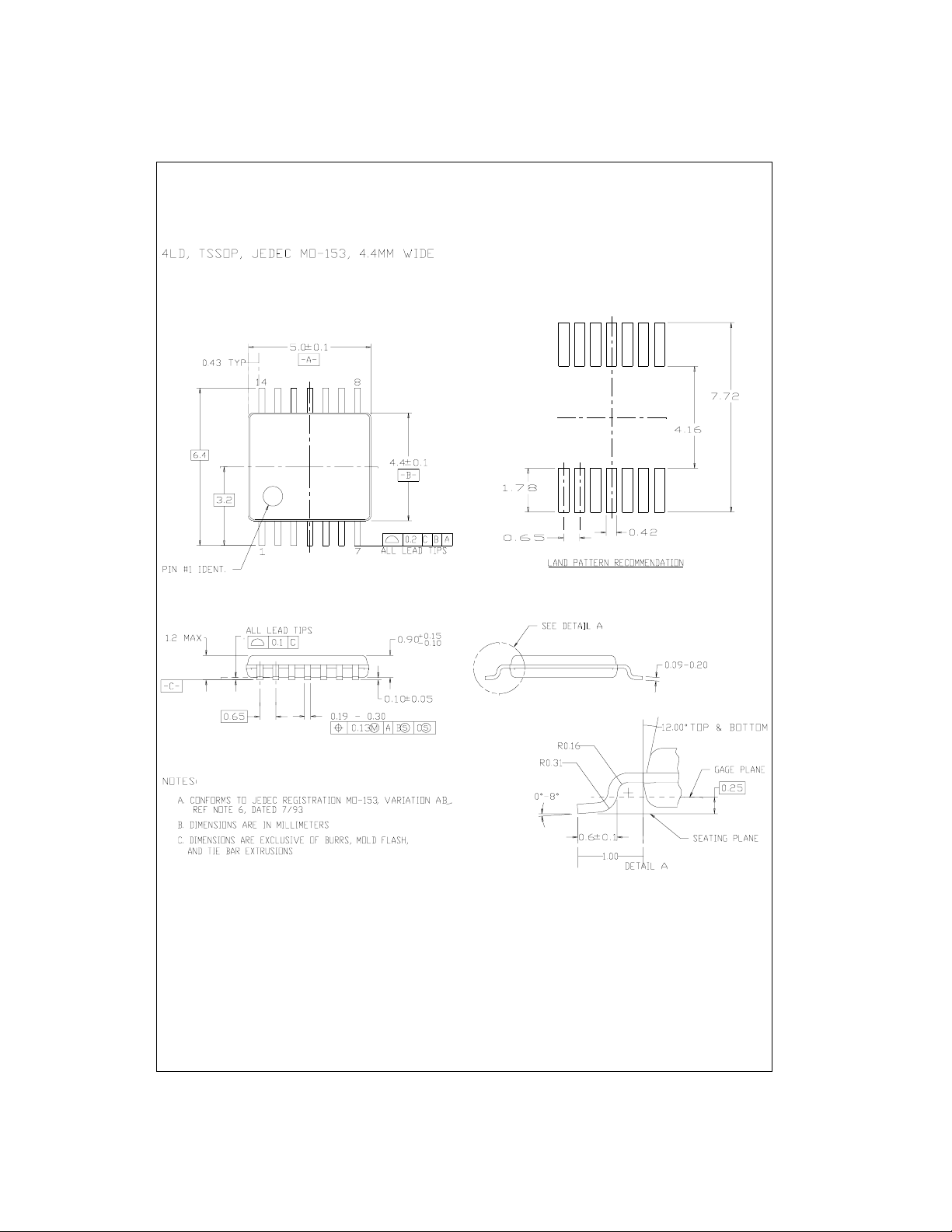
MM74HCT14MTC MTC14 14-Lead Thin Shrink Small Outline Package (TSSOP), JEDEC MO-153, 4.4mm Wide
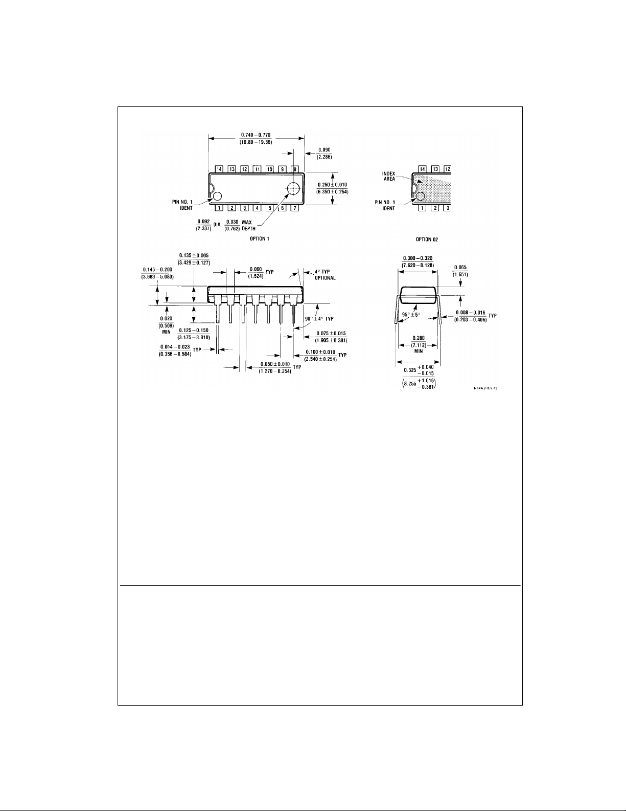
MM74HCT14N N14A 14-Lead Plastic Dual-In-Line Package (PDIP), JEDEC MS-001, 0.300” Wide
Devices also availab le in Tape and Reel. Specify by appending th e s uffix let t er “X” to the ordering code.
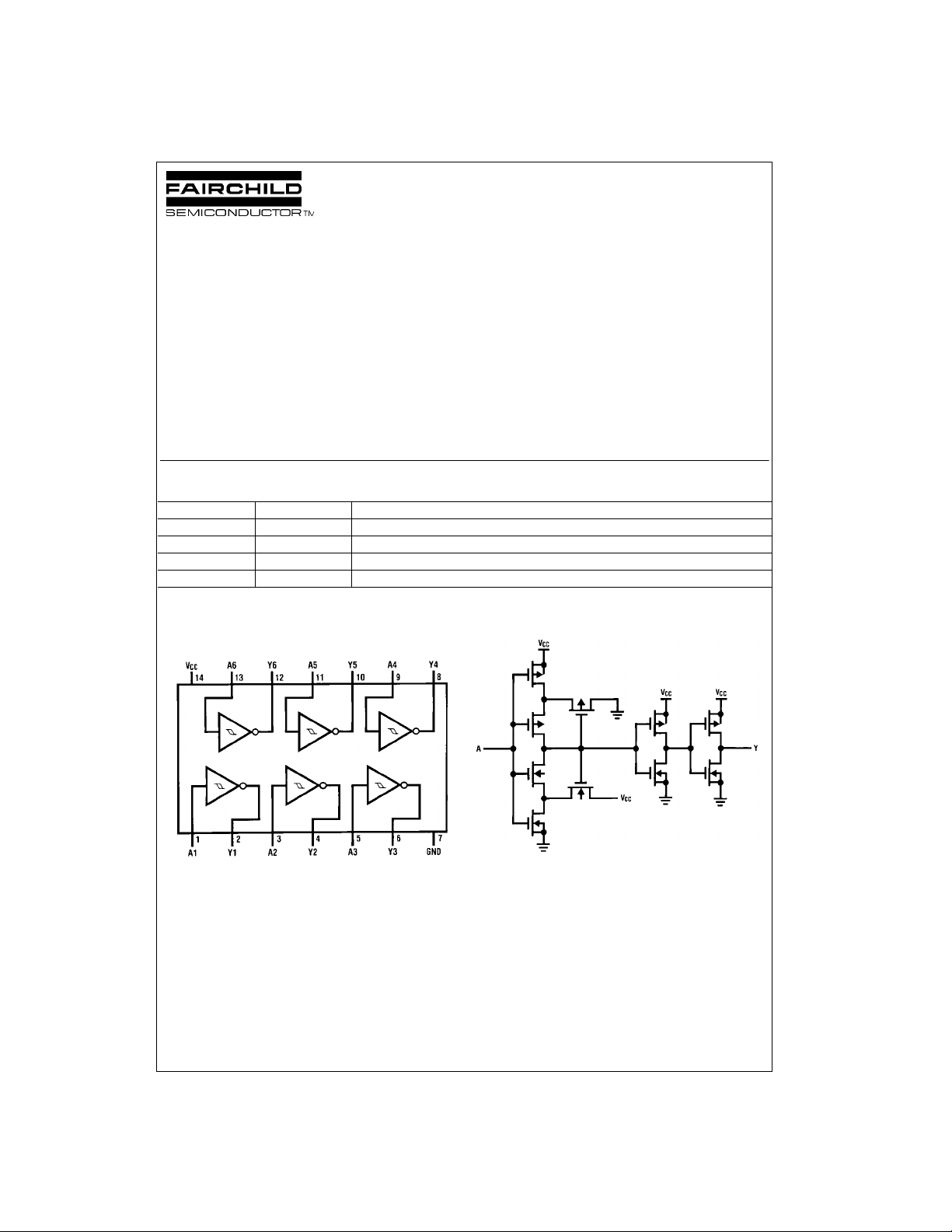
Connection Diagram
Pin Assignments for DIP, SOIC, SOP and TSSOP
Schematic Diagram
Top View
© 1999 Fairchild Semiconductor Corporation DS500059.prf www.fairchildsemi.com
Page 2
Absolute Maximum Ratings(Note 1)
(Note 2)
Supply Voltage (VCC) −0.5 to +7.0V
DC Input Voltage ( V
DC Output Voltage (V
MM74HCT14
Clamp Diode Current (I
DC Output Current, per pin (I
or GND Current, per pin (ICC) ± 50 mA
DC V
CC
Storage Temperature Range (T
Lead Temperature (T
) −1.5 to V
IN
) −0.5 to V
OUT
, IOK) ± 20 mA
IK
) ± 25 mA
OUT
) −65°C to +150°C
STG
)
L
CC
CC
+ 1.5V
+ 0.5V
Recommended Operating
Conditions
Min Max Units
Supply Voltage (V
DC Input or Output Voltage
, V
(V
IN
OUT
Operating Temperature Range (T
Note 1: Absolute Maximum Ratings are those values beyond which damage to the device may occur.
Note 2: Unless otherwise specified all voltages are refe renced to ground.
)26V
CC
)0V
) −40 +85 °C
A
CC
(Soldering 10 seconds) 260°C
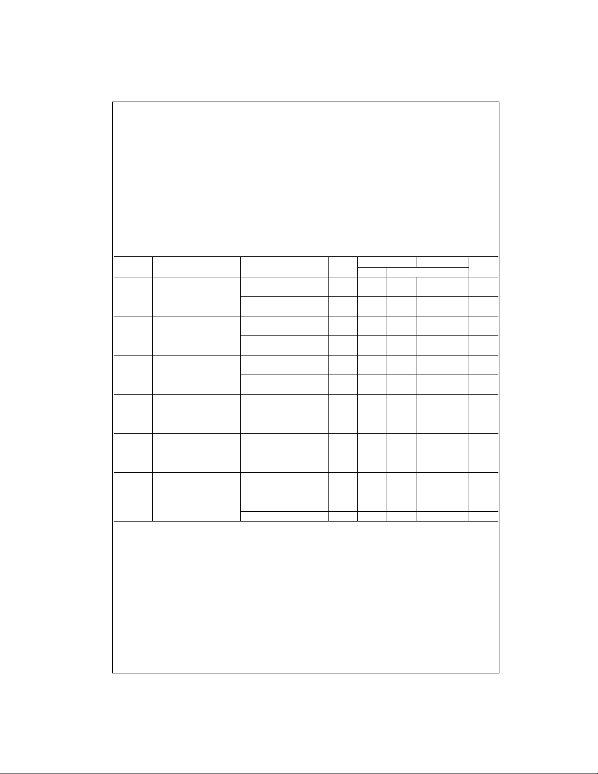
DC Electrical Characteristics (Note 3)
Symbol Parameter Conditions
V
T+
V
T−
V
H
V
OH
V
OL
I
IN
I
CC
Note 3: For a power su pply of 5V ± 10% t he worst cas e outpu t voltages (VOH, and VOL) occur for HC at 4.5V. Thus the 4.5V values shou ld be used when
designing with this supply. Worst case V
rent (I
Positive Going Minimum 4.5V 1.5 1.2 1.2 V
Threshold Voltage 5.5V 1.7 1.4 1.4 V
Negative Going Minimum 4.5V 0.9 0.5 0.5 V
Threshold Voltage 5.5V 1.0 0.6 0.6 V
Hysteresis Voltage Minimum 4.5V 0.6 0.4 0.4 V
Minimum HIGH Level VIN = V
Output Voltage |I
Maximum LOW Level VIN = V
Voltage |I
Maximum Input Current VIN = VCC or GND
Maximum Quiescent VIN = VCC or GND
Supply Current I
, ICC, and IOZ) occur for CMOS at the higher voltage and so th e 6. 0V values should be used.
IN
Maximum 4.5V 1.5 1.9 1.9 V
Maximum 4.5V 0.9 1.2 1.2 V
Maximum 4.5V 0.6 1.4 1.4 V
IL
| = 20 µAV
OUT
|I
| = 4.0 mA, VCC = 4.5V 4.2 3.98 3.84 V
OUT
|I
| = 4.8 mA, VCC = 5.5V 5.2 4.98 4.98 V
OUT
IH
| = 20 µA00.10.1V
OUT
|I
| = 4.0 mA, VCC = 4.5V 0.2 0.26 0.33 V
OUT
|I
| = 4.8 mA, VCC = 5.5V 0.2 0.26 0.33 V
OUT
VIH or V
IL
= 0 µA
OUT
VIN=2.4V or 0.5V (Note 3) 5.5V 2.4 2.4 mA
and VIL occur at VCC = 5.5V and 4.5V respectively. (The VIH value at 5.5V is 3.85V.) The worst case leakage cur-
IH
V
CC
5.5V 1.7 2.1 2.1 V
5.5V 1.0 1.4 1.4 V
5.5V 0.7 0.4 0.4 V
5.5V 0.7 1.5 1.5 V
5.5V 1.0 10 µA
TA = 25°CTA = −40 to 85°C
Typ Guaranteed Limits
CCVCC
− 0.1 VCC − 0.1 V
±0.1 ±1.0 µA
V
Units
www.fairchildsemi.com 2
Page 3
AC Electrical Characteristics
VCC = 5V, TA = 25°C, CL = 15 pF, tr = tf = 6 ns
Symbol Parameter Conditions Typ
t
PHL
, t
PLH
Maximum Propagation Delay 10 18 ns
Guaranteed
Limit
AC Electrical Characteristics
V
= 5V ± 10%, CL = 50 pF, tr = t
CC
Symbol Parameter Conditions
t
, t
PHL
t
, t
TLH
C
PD
C
IN
Note 4: CPD determines the no load dynamic power consumption, PD = CPD VCC2 f+ICC VCC, and the no load dynamic current consu m pt ion,
= CPDVCCf+ICC.
I
S
Maximum Propagation Delay 20 25 ns
PLH
Maximum Output Rise and Fall Time 9 15 19 ns
THL
Power Dissipation (per gate) 25 pF
Capacitance (Note 4)
Maximum Input Capacitance 5 10 10 pF
= 6 ns (unless otherwise specified)
f
TA = 25° TA = −40 to 85°C
Typ Guaranteed Limits
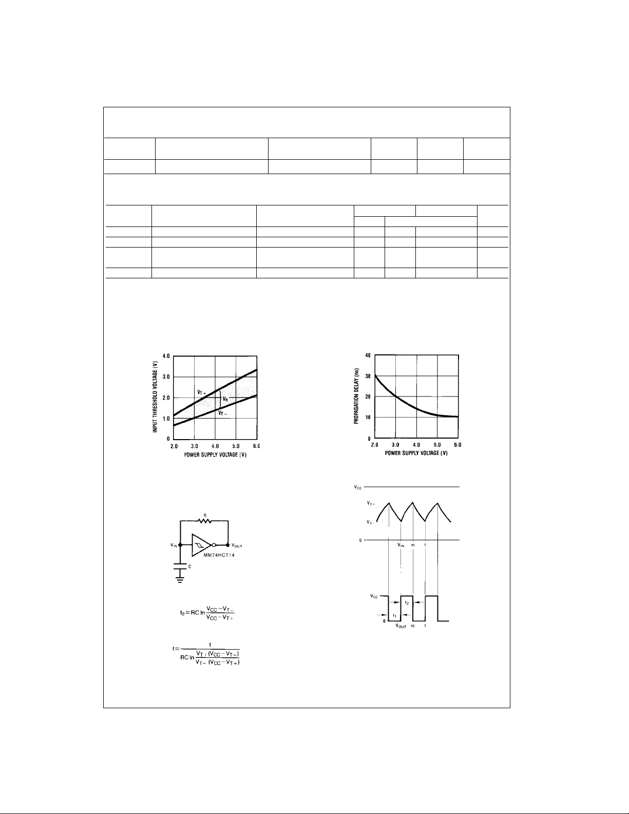
Typical Performance Characteristics
Input Threshold, V
+, VT−,
T
vs Power Supply Voltage
Propagation Delay vs
Power Supply
MM74HCT14
Units
Units
Typical Applications
Low Power Oscillator
Note: The equations assume t1+t2>>t
pd0+tpd1
3 www.fairchildsemi.com
Page 4
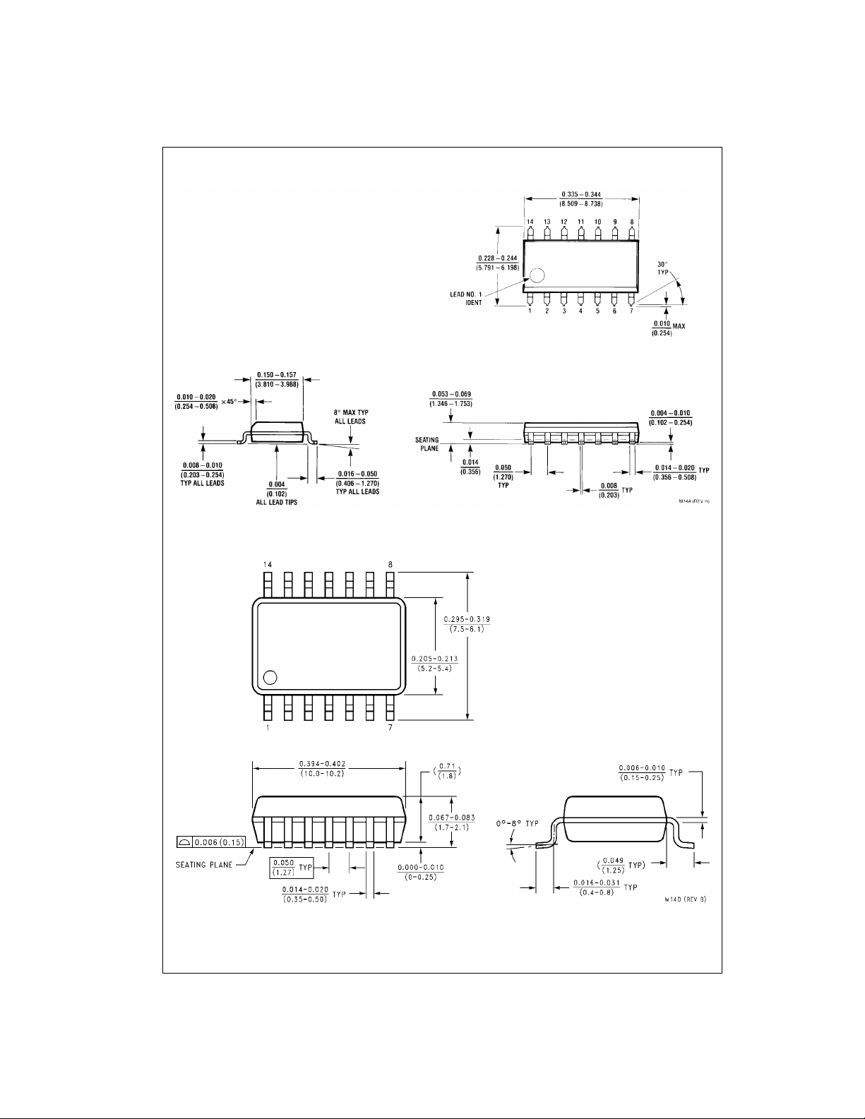
Physical Dimensions inches (millimeters) unless otherwise noted
MM74HCT14
14-Lead Small Outline Integrated Circuit (SOIC), JEDEC MS-120, 0.150” Narrow
14-Lead Small Outline Package ( SOP), EIAJ TYPE II, 5.3mm Wide
Package Number M14A
Package Number M14D
www.fairchildsemi.com 4
Page 5
Physical Dimensions inches (millimeters) unless otherwise noted (Continued)
MM74HCT14
14-Lead Thin Shrink Small Outline Package (TSSOP), JEDEC MO-153, 4.4mm Wide
Package Number MTC14
5 www.fairchildsemi.com
Page 6
Physical Dimensions inches (millimeters) unless otherwise noted (Continued)
MM74HCT14 Hex Inverting Schmitt Trigger
14-Lead Plastic Dual-In-Line Package (PDIP), JEDEC MS-001, 0.300” Wide
LIFE SUPPORT POLICY
FAIRCHILD’S PRODUCTS ARE NOT AUTHORIZED FOR USE AS CRITICAL COMPONENTS IN LIFE SUPPORT
DEVICES OR SYSTEMS WITHOUT THE EXPRESS WRITTEN APPROVAL OF THE PRESIDENT OF FAIRCHILD
SEMICONDUCTOR CORPORATION. As used herein:
1. Life support devices or systems are devices or syste ms
which, (a) are intended for surgical implant into the
body, or (b) support or sustain life, and (c) whose failure
to perform when properly used in accordance with
instructions for use provided in the labeling, can be reasonably expected to result in a significan t injury to the
user.
Package Number N14A
2. A critical component in any compon ent of a lif e supp ort
device or system whose failu re to perform can be reasonably expected to ca use the fa i lure of the li fe su pp ort
device or system, or to affect its safety or effectiveness.
www.fairchildsemi.com
Fairchild does not assume any responsibility for use of any circuitry described, no circuit patent licenses are implied and Fairchild reserves the right at any time without notice to change said circuitry and specifications.
 Loading...