

Datasheet MM74HCT138SJ, MM74HCT138SJX, MM74HCT138MX, MM74HCT138CW, MM74HCT138M Datasheet (Fairchild Semiconductor)
...Page 1
February 1984
Revised February 1999
MM74HCT138 3-to-8 Line Decoder
© 1999 Fairchild Semiconductor Corporation DS005362.prf www.fairchildsemi.com
MM74HCT138
3-to-8 Line Decoder
General Description
The MM74HCT138 decoder utilizes advanced silicon-gate
CMOS technology, and are well suited to memory address
decoding or data routi ng applic ations. Both c ircuits feature
high noise immunity and low power consumption usually
associat ed with CMOS circuitry, yet have speeds comparable to low power Schottky TTL logic.
The MM74HCT138 have 3 binar y select inpu ts (A, B, and
C). If the device is enabled these inputs deter mine which
one of the eight normally HIGH outputs will go LOW. Two
active LOW and one active HIGH enables (G1, G2A and
G2B) are provided to ease the cascading decoders.
The decoders’ output can drive 10 low power Schottky TTL
equivalent loads and are function ally and pin equi valent to
the 74LS138. All inputs a re p rotecte d from dam age d ue to
static discharge by diodes to V
CC
and ground.
MM74HCT devices are intended to interface between TTL
and NMOS components and standard CMOS devices.
These parts are also plug-in replacements for LS-TTL
devices and can be used to redu ce power consumption in
existing designs.
Features
■ TTL input compatible
■ Typical propagation delay: 20 ns
■ Low quiescent current: 80 µA maximum (74HCT Series)
■ Low input current: 1 µA maximum
■ Fanout of 10 LS-TTL loads
Ordering Code:
Devices also available in Tape and Reel. Specify by appending the suffix letter “X” to t he ordering code.
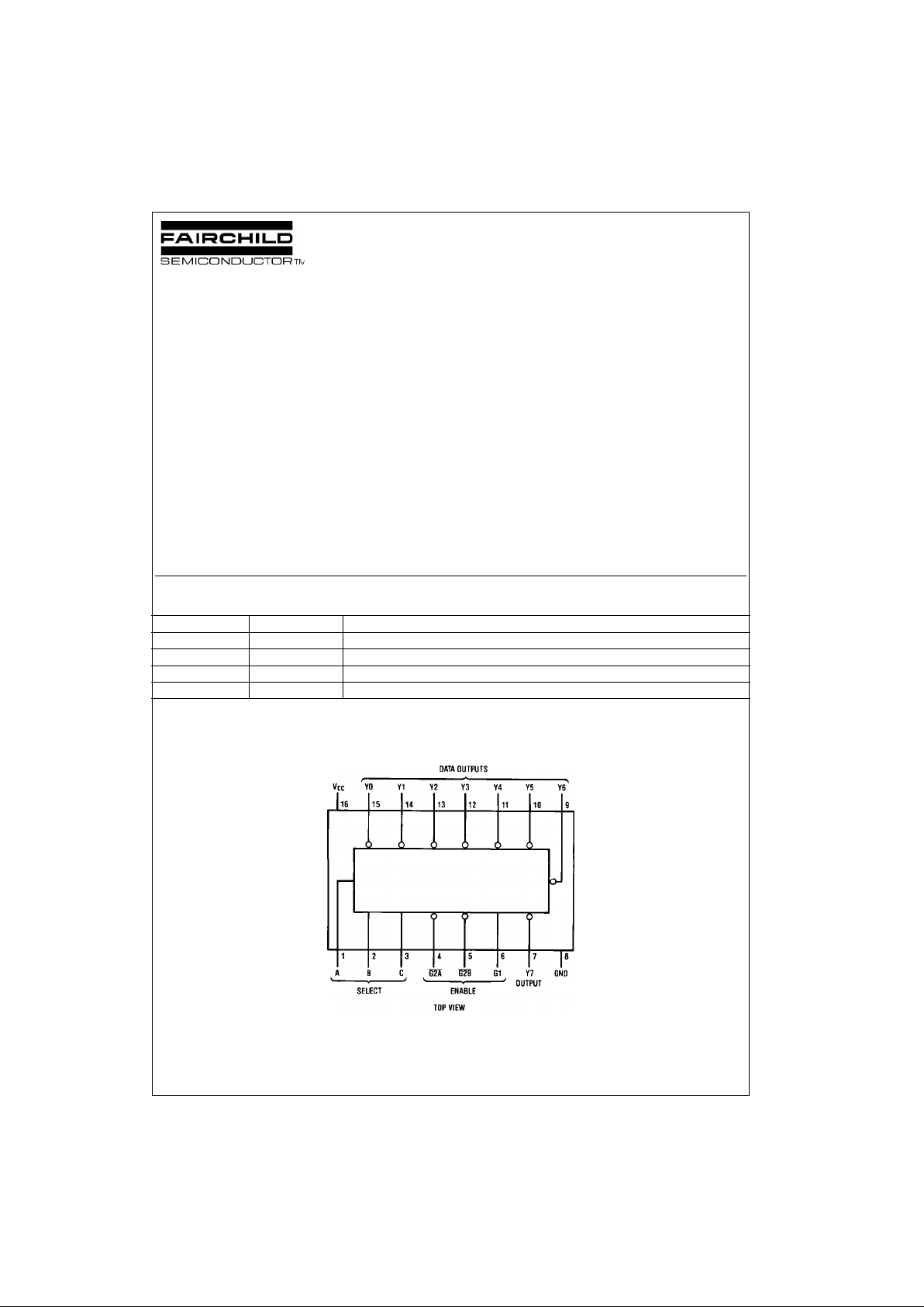
Connection Diagram
Pin Assignments for DIP, SOIC, SOP and TSSOP
Order Number Package Number Package Description
MM74HCT138M M16A 16-Lead Small Outline Integrated Circuit (SOIC), JEDEC MS-012, 0.150” Narrow
MM74HCT138SJ M16D 16-Lead Small Outline Package (SOP), EIAJ TYPE II, 5.3mm Wide
MM74HCT138MTC MTC16 16-Lead Thin Shrink Small Outline Package (TSSOP), JEDEC MO-153, 4.4mm W ide
MM74HCT138N N16E 16-Lead Plastic Dual-In-Line Package (PDIP), JEDEC MS-001, 0.300” Wide
Page 2
www.fairchildsemi.com 2
MM74HCT138
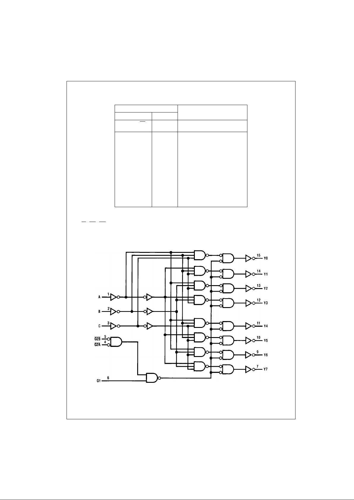
Truth Table
H = HIGH Level
L = LOW Lev el
X = Don’t Care
Note 1: G2
= G2A + G2B
Logic Diagram
Inputs Outputs
Enable Select
G1 G2
(Note 1)
C B A Y0 Y1 Y2 Y3 Y4 Y5 Y6 Y7
X H XXXHHHHHHHH
L X XXXHHHHHHHH
H L LLLLHHHHHHH
H L LLHHLHHHHHH
H L LHLHHLHHHHH
H L LHHHHHLHHHH
H L HLLHHHHLHHH
H L HLHHHHHHLHH
H L HHLHHHHHHLH
H L HHHHHHHHHHL
Page 3
3 www.fairchildsemi.com
MM74HCT138
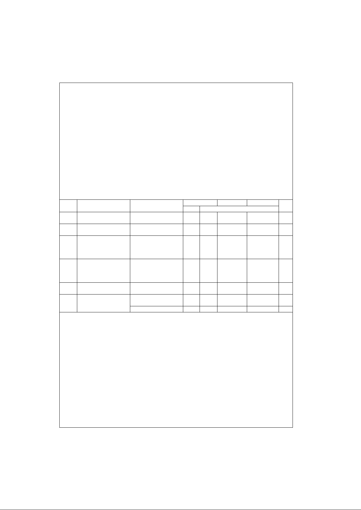
Absolute Maximum Ratings(Note 2)
(Note 3)
Recommended Operating
Conditions
Note 2: Absolute Maximum Rati ngs are tho se values b eyond which d am-
age to the device may occur.
Note 3: Unless otherwise specified all voltages are referenced to ground.
Note 4: Power Dissipation temperature de rating — p lastic “N” p ackage: −
12 mW/°C from 65°C to 85°C.
DC Electrical Characteristics
V
CC
= 5V ±10% (unless otherwise specified)
Note 5: This is measured per input pin. All othe r inputs are held at VCC or ground.
Supply Voltage (VCC) −0.5 to +7.0V
DC Input Voltage (V
IN
) −1.5 to V
CC
+1.5V
DC Output Voltage (V
OUT
) −0.5 to V
CC
+0.5V
Clamp Diode Current (I
IK
, IOK) ±20 mA
DC Output Current, per pin (I
OUT
) ±25 mA
DC V
CC
or GND Current, per pin (ICC) ±50 mA
Storage Temperature Range (T
STG
) −65°C to +150°C
Power Dissipation (P
D
)
(Note 4) 600 mW
S.O. Package only 500 mW
Lead Temperature (T
L
)
(Soldering 10 seconds) 260°C
Min Max Units
Supply Voltage (V
CC
)4.55.5V
DC Input or Output Voltage
(V
IN
, V
OUT
)0V
CC
V
Operating Temperature Range (T
A
) −40 +85 °C
Input Rise or Fall Times
(t
r
, tf) 500 ns
Symbol Parameter Conditions
TA = 25°CTA = −40 to 85°CTA = −55 to 125°C
Units
Typ Guaranteed Limits
V
IH
Minimum HIGH Level 2.0 2.0 2.0 V
Input Voltage
V
IL
Maximum LOW Level 0.8 0.8 0.8 V
Input Voltage
V
OH
Minimum HIGH Level V
IN
= VIH or V
IL
Output Voltage |I
OUT
| = 20 µAV
CCVCC
− 0.1 VCC− 0.1 VCC− 0.1 V
|I
OUT
| = 4.0 mA, V
CC
= 4.5V 4.2 3.98 3.84 3.7 V
|I
OUT
| = 4.8 mA, V
CC
= 5.5V 5.2 4.98 4.84 4.7 V
V
OL
Maximum LOW Level V
IN
= VIH or V
IL
Voltage |I
OUT
| = 20 µA 0 0.1 0.1 0.1 V
|I
OUT
| = 4.0 mA, V
CC
= 4.5V 0.2 0.26 0.33 0.4 V
|I
OUT
| = 4.8 mA, V
CC
= 5.5V 0.2 0.26 0.33 0.4 V
I
IN
Maximum Input V
IN
= VCC or GND, ±0.1 ±1.0 ±1.0 µA
Current VIH or V
IL
I
CC
Maximum Quiescent V
IN
= VCC or GND 8.0 80 160 µA
Supply Current I
OUT
= 0 µA
V
IN
= 2.4V or 0.5V (Note 5) 0.3 0.4 0.5 mA
Page 4

www.fairchildsemi.com 4
MM74HCT138
AC Electrical Charac teristics
T
A
= 25°C, V
CC
= 5.0V, tr = tf = 6 ns, C
L
= 15 pF (unless otherwise specified)
AC Electrical Charac teristics
V
CC
= 5V ± 10%, CL = 50 pF, tr = t
f
= 6 ns (unless otherwise specified)
Note 6: CPD determines the no load dynamic power consumption, PD = CPD V
CC
2
f + ICC VCC, and the no load dynamic current consum pt ion,
I
S
= CPDVCCf + ICC.
Symbol Parameter Conditions Typ
Guaranteed
Units
Limit
t
PHL
Maximum Propagation Delay, A, B, or C to Output 20 35 ns
t
PLH
Maximum Propagation Delay, A, B, or C to Output 13 25 ns
t
PHL
Maximum Propagation Delay, G1 to Y Output 14 25 ns
t
PLH
Maximum Propagation Delay, G1 to Y Output 13 25 ns
t
PHL Maximum Propagation Delay, G2A or G2B to Y Output
17 30 ns
t
PLH Maximum Propagation Delay, G2A or G2B to Y Output
13 25 ns
Symbol Parameter Conditions
TA = 25°CTA = −40 to 85°CTA = −55 to 125°C
Units
Typ Guaranteed Limits
t
PHL
Maximum Propagation Delay 24 40 50 60 ns
A, B, or C to Output
t
PLH
Maximum Propagation Delay 18 30 38 45 ns
A, B, or C to Output
t
PHL
Maximum Propagation Delay 17 30 38 45 ns
G1 to Y Output
t
PLH
Maximum Propagation Delay 20 30 38 45 ns
G1 to Y Output
t
PHL
Maximum Propagation Delay 23 35 43 52 ns
G2A or G2B to Y Output
t
PLH
Maximum Propagation Delay 18 30 38 45 ns
G2A or G2B to Y Output
t
THL
, t
TLH
Maximum Output 15 19 22 ns
Rise and Fall Time
C
IN
Input Capacitance 5 10 10 pF
C
PD
Power Dissipation 55 pF
Capacitance (Note 6)
Page 5

5 www.fairchildsemi.com
MM74HCT138
Physical Dimensions inches (millimeters) unless otherwise noted
16-Lead Small Outline Integrated Circuit (SOIC), JEDEC MS-012, 0.150” Narrow
Package Number M16A
16-Lead Small Outline Package (SOP), EIAJ TYPE II, 5.3mm Wide
Package Number M16D
Page 6

www.fairchildsemi.com 6
MM74HCT138
Physical Dimensions inches (millimeters) unless otherwise noted (Continued)
16-Lead Thin Shrink Small Outline Package (TSSOP), JEDEC MO-153, 4.4mm Wide
Package Number MTC16
Page 7

Fairchild does not assume any responsibility for use of any circuitry descri bed, no circuit patent licenses are implied and Fairchild reser ves the right at any time without notice to change said circuitr y and specifications.
MM74HCT138 3-to-8 Line Decoder
LIFE SUPPORT POLICY
FAIRCHILD’S PRODUCTS ARE NOT AUTHORIZED FOR USE AS CRITICAL COMPONENTS IN LIFE SUPPORT
DEVICES OR SYSTEMS WITHOUT THE EXPRESS WRITTEN APPROVAL OF THE PRESIDENT OF FAIRCHILD
SEMICONDUCTOR CORPORATION. As used herein:
1. Life support devices or system s a re devices or syste ms
which, (a) are intended for surgical implant into the
body, or (b) support or sustain life, and (c) whose failure
to perform when properly used in accordance with
instructions for use provided in the labeling, can be reasonably expected to result in a significant injur y to the
user.
2. A critical compon ent in any com ponent of a li fe support
device or system whose failure to p erform can be r easonably expected to cause the failure of the life suppor t
device or system, or to affect its safety or effectiveness.
www.fairchildsemi.com
Physical Dimensions inches (millimeters) unless otherwise noted (Continued)
16-Lead Plastic Dual-In-Line Package (PDIP), JEDEC MS-001, 0.300” Wide
Package Number N16E
 Loading...