

Datasheet MM74HC74ASJX, MM74HC74ACW, MM74HC74AM, MM74HC74AMTC, MM74HC74AMTCX Datasheet (Fairchild Semiconductor)
...Page 1
September 1983
Revised February 1999
MM74HC74A Dual D-Type Flip-Flop with Preset and Clear
© 1999 Fairchild Semiconductor Corporation DS005106.prf www.fairchildsemi.com
MM74HC74A
Dual D-Type Flip-Flop with Preset and Clear
General Description
The MM74HC74A utilizes advanced silicon-gate CMOS
technology to achieve operating speeds similar to the
equivalent LS-TTL part. It pos sesse s the high no ise imm unity and low power consumpti on of standard CMOS integrated circuits, along with the ability to drive 1 0 LS-TTL
loads.
This flip-flop has independent data, preset, clear, and clock
inputs and Q and Q
outputs. The logic level present at the
data input is transferred to the outp ut during the positivegoing transition of the clock pulse. Preset and clear are
independent of the clock a nd accomplish ed by a low level
at the appropriate input.
The 74HC logic family is functionally and pinout compatible
with the standard 74LS logic family. All inputs are protected
from damage due to static discharge by internal diode
clamps to V
CC
and ground.
Features
■ Typical propagation delay: 20 ns
■ Wide power supply range: 2–6V
■ Low quiescent current: 40 µA maximum (74HC Series)
■ Low input current: 1 µA maximum
■ Fanout of 10 LS-TTL loads
Ordering Code:
Devices also availab le in Tape and Reel. Specify by appending th e s uffix let t er “X” to the ordering cod e.
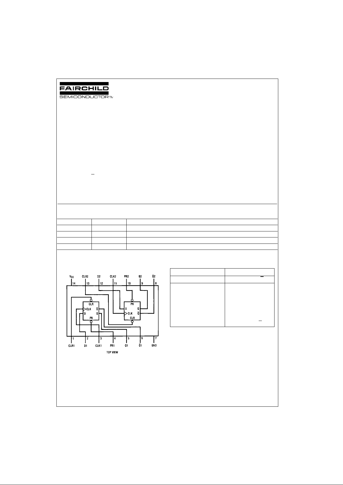
Connection Diagram
Pin Assignments f or DIP, SOIC, SOP and TSSOP
Truth Table
Note: Q0 = the level of Q before the indica t ed input condition s w ere estab-
lished.
Note 1: This configuration i s no nst able; tha t is, i t will n ot pe rsis t whe n p re-
set and clear inputs ret urn to their inactive (HI GH ) level.
Order Number Package Number Package Description
MM74HC74AM M14A 14-Lead Small Outline Integrated Circuit (SOIC), JEDEC MS-120, 0.150” Narrow
MM74HC74ASJ M14D 14-Lead Small Outline Package (SOP), EIAJ TYPE II, 5.3mm Wide
MM74HC74AMTC MTC14 14-Lead Thin Shrink Small Outline Package (TSSOP), JEDEC MO-153, 4.4mm Wide
MM74HC74AN N14A 14-Lead Plastic Dual-In-Line Package (PDIP), JEDEC MS-001, 0.300” Wide
Inputs Outputs
PR CLR CLK D Q Q
LHXX H L
HL XX L H
L L X X H (Note 1) H (Note 1)
HH ↑ HH L
HH ↑ LL H
HH LX Q0 Q
0
Page 2
www.fairchildsemi.com 2
MM74HC74A
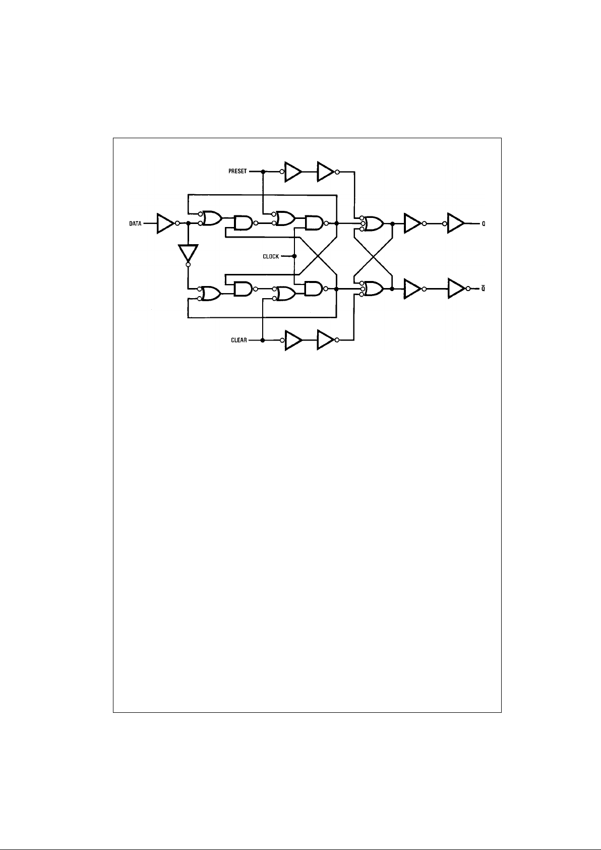
Logic Diagram
Page 3
3 www.fairchildsemi.com
MM74HC74A
Absolute Maximum Ratings(Note 2)
(Note 3)
Recommended Operating
Conditions
Note 2: Absolute Maximum Ra tings are those valu es beyond w hich dam-
age to the device may occur.
Note 3: Unless otherwise specified all voltages are referenced to ground.
Note 4: Power Dissipation te mperature d erating — pl astic “N” pa ckage: −
12 mW/°C from 65°C to 85°C.
DC Electrical Characteristics (Note 5)
Note 5: For a powe r supply o f 5V ±10% the worst case output voltages (VOH, and VOL) occur for HC at 4.5V. Thus the 4. 5V valu es shou ld be u sed when
designing with this supply. Worst case V
IH
and VIL occur at V
CC
= 5.5V and 4.5V respectively. (The VIH value at 5.5V is 3 .8 5V.) The worst c as e leakage cur-
rent (I
IN
, ICC, and IOZ) occur for CMOS at the higher voltage and so th e 6. 0V values should be used.
Supply Voltage (VCC) −0.5 to +7.0V
DC Input Voltage (V
IN
) −1.5 to V
CC
+1.5V
DC Output Voltage (V
OUT
) −0.5 to V
CC
+0.5V
Clamp Diode Current (I
IK
, IOK) ±20 mA
DC Output Current, per pin (I
OUT
) ±25 mA
DC V
CC
or GND Current, per pin
(I
CC
) ±50 mA
Storage Temperature Range (T
STG
) −65°C to +150°C
Power Dissipation (P
D
)
(Note 4) 600 mW
S.O. Package only 500 mW
Lead Temperature (T
L
)
(Soldering 10 seconds) 260°C
Min Max Units
Supply Voltage (V
CC
)26V
DC Input or Output Voltage 0 V
CC
V
(V
IN, OUT
)
Operating Temperature Range (T
A
) −40 +85 °C
Input Rise or Fall Times
(t
r
, tf) V
CC
= 2.0V 1000 ns
V
CC
= 4.5V 500 ns
V
CC
= 6.0V 400 ns
Symbol Parameter Conditions
V
CC
TA = 25°CTA = −40 to 85°CTA = −55 to 125°C
Units
Typ Guaranteed Limits
V
IH
Minimum HIGH Level 2.0V 1.5 1.5 1.5 V
Input Voltage 4.5V 3.15 3.15 3.15 V
6.0V 4.2 4.2 4.2 V
V
IL
Maximum LOW Level 2.0V 0.5 0.5 0.5 V
Input Voltage 4.5V 1.35 1.35 1.35 V
6.0V 1.8 1.8 1.8 V
V
OH
Minimum HIGH Level V
IN
= VIH or V
IL
Output Voltage |I
OUT
| ≤ 20 µA 2.0V 2.0 1.9 1.9 1.9 V
4.5V 4.5 4.4 4.4 4.4 V
6.0V 6.0 5.9 5.9 5.9 V
VIN = VIH or V
IL
|I
OUT
| ≤ 4.0 mA 4.5V 4.3 3.98 3.84 3.7 V
|I
OUT
| ≤ 5.2 mA 6.0V 5.2 5.48 5.34 5.2 V
V
OL
Maximum LOW Level V
IN
= VIH or V
IL
Output Voltage |I
OUT
| ≤ 20 µA 2.0V 0 0.1 0.1 0.1 V
4.5V 0 0.1 0.1 0.1 V
6.0V 0 0.1 0.1 0.1 V
V
IN
= VIH or V
IL
|I
OUT
| ≤ 4.0 mA 4.5V 0.2 0.26 0.33 0.4 V
|I
OUT
| ≤ 5.2 mA 6.0V 0.2 0.26 0.33 0.4 V
I
IN
Maximum Input V
IN
= VCC or GND 6.0V ±0.1 ±1.0 ±1.0 µA
Current
I
CC
Maximum Quiescent V
I N =VCC
or GND 6.0V 4.0 40 80 µA
Supply Current I
OUT
= 0 µA
Page 4

www.fairchildsemi.com 4
MM74HC74A
AC Electrical Characteristics
V
CC
= 5V, T
A
= 25°C, CL = 15 pF, t
r
= t
f
= 6 ns
AC Electrical Characteristics
C
L
= 50 pF, tr = t
f
= 6 ns (unless otherwise specified)
Note 6: CPD determines the no lo ad dynamic power con s um ption, PD = CPD V
CC
2
f + ICC VCC, and the no load dynam ic c urrent consumption ,
I
S
= CPDVCCf + ICC.
Symbol Parameter Conditions Typ
Guaranteed
Units
Limit
f
MAX
Maximum Operating Frequency 72 30 MHz
t
PHL
, t
PLH
Maximum Propagation 10 30 ns
Delay Clock to Q or Q
t
PHL
, t
PLH
Maximum Propagation 17 40 ns
Delay Preset or Clear to Q or Q
t
REM
Minimum Removal Time, 6 5 ns
Preset or Clear to Clock
t
s
Minimum Setup Time 10 20 ns
Data to Clock
t
H
Minimum Hold Time 0 0 ns
Clock to Data
t
W
Minimum Pulse Width 8 16 ns
Clock, Preset or Clear
Symbol Parameter Conditions
V
CC
TA = 25°CTA = −40 to 85°CTA = −55 to 125°C
Units
Typ Guaranteed Limits
f
MAX
Maximum Operating 2.0V 22 6 5 4 MHz
Frequency 4.5V 72 30 24 20 MHz
6.0V 94 35 28 24 MHz
t
PHL
, t
PLH
Maximum Propagation 2.0V 34 110 140 165 ns
Delay Clock to Q or Q
4.5V 12 22 28 33 ns
6.0V 10 19 24 28 ns
t
PHL
, t
PLH
Maximum Propagation 2.0V 66 150 190 225 ns
Delay Preset or Clear 4.5V 20 30 38 45 ns
To Q or Q
6.0V 16 26 33 38 ns
t
REM
Minimum Removal Time 2.0V 20 50 65 75 ns
Preset or Clear 4.5V 6 10 13 15 ns
To Clock 6.0V 5 9 11 13 ns
t
s
Minimum Setup Time 2.0V 35 80 100 120 ns
Data to Clock 4.5V 10 16 20 24 ns
6.0V 8 14 17 20 ns
t
H
Minimum Hold Time 2.0V 0 0 0 ns
Clock to Data 4.5V 0 0 0 ns
6.0V 0 0 0 ns
t
W
Minimum, Pulse Width 2.0V 30 80 101 119 ns
Clock, Preset or Clear 4.5V 9 16 20 24 ns
6.0V 8 14 17 20 ns
t
TLH
, t
THL
Maximum Output 2.0V 25 75 95 110 ns
Rise and Fall Time 4.5V 7 15 19 22 ns
6.0V 6 13 16 19 ns
tr, t
f
Maximum Input Rise 2.0V 1000 1000 1000 ns
and Fall Time 4.5V 500 500 500 ns
6.0V 400 400 400 ns
C
PD
Power Dissipation (per flip-flop) 80 pF
Capacitance (Note 6)
C
IN
Maximum Input 5 10 10 10 pF
Capacitance
Page 5

5 www.fairchildsemi.com
MM74HC74A
Physical Dimensions inches (millimeters) unless otherwise noted
14-Lead Small Outline Integrated Circuit (SOIC), JEDEC MS-120, 0.150” Narrow
Package Number M14A
14-Lead Small Outline Package (SOP), EIAJ TYPE II, 5.3mm Wide
Package Number M14D
Page 6
www.fairchildsemi.com 6
MM74HC74A
Physical Dimensions inches (millimeters) unless otherwise noted (Continued)
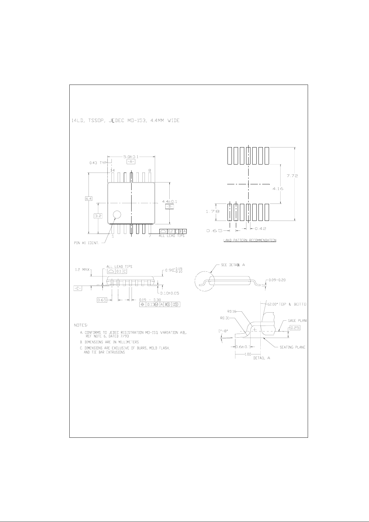
14-Lead Thin Shrink Small Outline Package (TSSOP), JEDEC MO-153, 4.4mm Wide
Package Number MTC14
Page 7

Fairchild does not assume any responsibility for use of any circuitry described, no circuit patent licenses are implied and Fairchild reserves the right at any time without notice to change said circuitry and specifications.
MM74HC74A Dual D-Type Flip-Flop with Preset and Clear
LIFE SUPPORT POLICY
FAIRCHILD’S PRODUCTS ARE NOT AUTHORIZED FOR USE AS CRITICAL COMPONENTS IN LIFE SUPPORT
DEVICES OR SYSTEMS WITHOUT THE EXPRESS WRITTEN APPROVAL OF THE PRESIDENT OF FAIRCHILD
SEMICONDUCTOR CORPORATION. As used herein:
1. Life support devices or systems are devices or systems
which, (a) are intended for surgical implant into the
body, or (b) support or sustain life, and (c) whose failure
to perform when properly used in accordance with
instructions for use provided i n the labe li ng, can be re asonably expected to result in a significant injury to the
user.
2. A critical component in any com ponen t of a life s uppor t
device or system whose failu re to perform can b e reasonably expected to c ause th e fa i lure of the li fe s upp or t
device or system, or to affect its safety or effectiveness.
www.fairchildsemi.com
Physical Dimensions inches (millimeters) unless otherwise noted (Continued)
14-Lead Plastic Dual-In-Line Package (PDIP), JEDEC MS-001, 0.300” Wide
Package Number N14A
 Loading...